AD7708/AD7718 8-/10-Channel, Low Voltage, Low Power ... - Micros
AD7708/AD7718 8-/10-Channel, Low Voltage, Low Power ... - Micros
AD7708/AD7718 8-/10-Channel, Low Voltage, Low Power ... - Micros

You also want an ePaper? Increase the reach of your titles
YUMPU automatically turns print PDFs into web optimized ePapers that Google loves.
a<br />
FEATURES<br />
8-/<strong>10</strong>-<strong>Channel</strong>, High Resolution - ADCs<br />
<strong>AD7708</strong> Has 16-Bit Resolution<br />
<strong>AD7718</strong> Has 24-Bit Resolution<br />
Factory-Calibrated<br />
Single Conversion Cycle Setting<br />
Programmable Gain Front End<br />
Simultaneous 50 Hz and 60 Hz Rejection<br />
VREF Select Allows Absolute and Ratiometric<br />
Measurement Capability<br />
Operation Can Be Optimized for<br />
Analog Performance (CHOP = 0) or<br />
<strong>Channel</strong> Throughput (CHOP = 1)<br />
INTERFACE<br />
3-Wire Serial<br />
SPI TM , QSPI TM , MICROWIRE TM , and DSP-Compatible<br />
Schmitt Trigger on SCLK<br />
POWER<br />
Specified for Single 3 V and 5 V Operation<br />
Normal: 1.28 mA Typ @ 3 V<br />
<strong>Power</strong>-Down: 30 A (32 kHz Crystal Running)<br />
On-Chip Functions<br />
Rail-to-Rail Input Buffer and PGA<br />
2-Bit Digital I/O Port<br />
APPLICATIONS<br />
Industrial Process Control<br />
Instrumentation<br />
Pressure Transducers<br />
Portable Instrumentation<br />
Smart Transmitters<br />
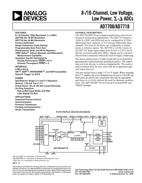
FUNCTIONAL BLOCK DIAGRAM<br />
8-/<strong>10</strong>-<strong>Channel</strong>, <strong>Low</strong> <strong>Voltage</strong>,<br />
<strong>Low</strong> <strong>Power</strong>, - ADCs<br />
<strong>AD7708</strong>/<strong>AD7718</strong><br />
GENERAL DESCRIPTION<br />
The <strong>AD7708</strong>/<strong>AD7718</strong> are complete analog front-ends for low<br />
frequency measurement applications. The <strong>AD7718</strong> contains a<br />
24-bit Σ-∆ ADC with PGA and can be configured as 4/5 fullydifferential<br />
input channels or 8/<strong>10</strong> pseudo-differential input<br />
channels. Two pins on the device are configurable as analog<br />
inputs or reference inputs. The <strong>AD7708</strong> is a 16-bit version of<br />
the <strong>AD7718</strong>. Input signal ranges from 20 mV to 2.56 V can be<br />
directly converted using these ADCs. Signals can be converted<br />
directly from a transducer without the need for signal conditioning.<br />
The device operates from a 32 kHz crystal with an on-board PLL<br />
generating the required internal operating frequency. The output<br />
data rate from the part is software programmable. The peak-topeak<br />
resolution from the part varies with the programmed gain<br />
and output data rate.<br />
The part operates from a single 3 V or 5 V supply. When operating<br />
from 3 V supplies, the power dissipation for the part is 3.84 mW typ.<br />
Both parts are pin-for-pin compatible allowing an upgradable<br />
path from 16 to 24 bits without the need for hardware modifications.<br />
The <strong>AD7708</strong>/<strong>AD7718</strong> are housed in 28-lead SOIC and<br />
TSSOP packages.<br />
DVDD<br />
DGND<br />
REFIN2(+)/AIN9 REFIN1(+) REFIN2(–)/AIN<strong>10</strong> REFIN1(–)<br />
XTAL1 XTAL2<br />
AIN1<br />
AIN2<br />
AIN3<br />
AIN4<br />
AIN5<br />
AIN6<br />
AIN7<br />
AIN8<br />
AINCOM<br />
MUX<br />
NEG BUF<br />
POS BUF<br />
PGA<br />
REFIN(+)<br />
- ADC*<br />
REFIN(–)<br />
*<strong>AD7708</strong> 16-BIT ADC<br />
*<strong>AD7718</strong> 24-BIT ADC<br />
AVDD<br />
OSC<br />
AND<br />
PLL<br />
SERIAL<br />
INTERFACE<br />
AND<br />
CONTROL<br />
LOGIC<br />
DOUT<br />
DIN<br />
SCLK<br />
CS<br />
RDY<br />
RESET<br />
<strong>AD7708</strong>/<strong>AD7718</strong><br />
I/O PORT<br />
AVDD<br />
AGND<br />
SPI and QSPI are trademarks of Motorola Inc.<br />
MICROWIRE is a trademark of National Semiconductor Corp.<br />
VREF Select is a trademark of Analog Devices, Inc.<br />
REV. 0<br />
Information furnished by Analog Devices is believed to be accurate and<br />
reliable. However, no responsibility is assumed by Analog Devices for its<br />
use, nor for any infringements of patents or other rights of third parties that<br />
may result from its use. No license is granted by implication or otherwise<br />
under any patent or patent rights of Analog Devices.<br />
P2 P1<br />
One Technology Way, P.O. Box 9<strong>10</strong>6, Norwood, MA 02062-9<strong>10</strong>6, U.S.A.<br />
Tel: 781/329-4700<br />
www.analog.com<br />
Fax: 781/326-8703 © Analog Devices, Inc., 2001
<strong>AD7708</strong>/<strong>AD7718</strong><br />
TABLE OF CONTENTS<br />
FEATURES . . . . . . . . . . . . . . . . . . . . . . . . . . . . . . . . . . . . . 1<br />
FUNCTIONAL BLOCK DIAGRAM . . . . . . . . . . . . . . . . . 1<br />
GENERAL DESCRIPTION . . . . . . . . . . . . . . . . . . . . . . . . . 1<br />
<strong>AD7718</strong> SPECIFICATIONS . . . . . . . . . . . . . . . . . . . . . . . . 3<br />
<strong>AD7708</strong> SPECIFICATIONS . . . . . . . . . . . . . . . . . . . . . . . . 6<br />
TIMING CHARACTERISTICS . . . . . . . . . . . . . . . . . . . . . 9<br />
ABSOLUTE MAXIMUM RATINGS . . . . . . . . . . . . . . . . <strong>10</strong><br />
ORDERING GUIDE . . . . . . . . . . . . . . . . . . . . . . . . . . . . . <strong>10</strong><br />
PIN FUNCTION DESCRIPTIONS . . . . . . . . . . . . . . . . . 12<br />
PIN CONFIGURATION . . . . . . . . . . . . . . . . . . . . . . . . . . 13<br />
ADC CIRCUIT INFORMATION . . . . . . . . . . . . . . . . . . . 15<br />
Signal Chain Overview (CHOP Enabled, CHOP = 0) . . . 15<br />
ADC NOISE PERFORMANCE CHOP ENABLED<br />
(CHOP = 0) . . . . . . . . . . . . . . . . . . . . . . . . . . . . . . . . . . . 17<br />
Signal Chain Overview (CHOP Disabled CHOP = 1) . . . 19<br />
ADC NOISE PERFORMANCE CHOP DISABLED<br />
(CHOP = 1) . . . . . . . . . . . . . . . . . . . . . . . . . . . . . . . . . . . 20<br />
ON-CHIP REGISTERS . . . . . . . . . . . . . . . . . . . . . . . . . . . 22<br />
Communications Register . . . . . . . . . . . . . . . . . . . . . . . . . . 25<br />
Status Register . . . . . . . . . . . . . . . . . . . . . . . . . . . . . . . . . . . 26<br />
Mode Register . . . . . . . . . . . . . . . . . . . . . . . . . . . . . . . . . . . 27<br />
Operating Characteristics when Addressing the<br />
Mode and Control Registers . . . . . . . . . . . . . . . . . . . . . . . 28<br />
ADC Control Register . . . . . . . . . . . . . . . . . . . . . . . . . . . . . 28<br />
Filter Register . . . . . . . . . . . . . . . . . . . . . . . . . . . . . . . . . . . 29<br />
I/O Control Register . . . . . . . . . . . . . . . . . . . . . . . . . . . . . . 30<br />
ADC Data Result Register . . . . . . . . . . . . . . . . . . . . . . . . . . 30<br />
Unipolar Mode . . . . . . . . . . . . . . . . . . . . . . . . . . . . . . . . . . 30<br />
Bipolar Mode . . . . . . . . . . . . . . . . . . . . . . . . . . . . . . . . . . . . 31<br />
ADC Offset Calibration Coefficient Registers . . . . . . . . . . . 31<br />
ADC Gain Calibration Coefficient Register . . . . . . . . . . . . . 31<br />
ID Register (ID) . . . . . . . . . . . . . . . . . . . . . . . . . . . . . . . . . 31<br />
User Nonprogrammable Test Registers . . . . . . . . . . . . . . . . 31<br />
Configuring the <strong>AD7708</strong>/<strong>AD7718</strong> . . . . . . . . . . . . . . . . . . . . 32<br />
DIGITAL INTERFACE . . . . . . . . . . . . . . . . . . . . . . . . . . . 34<br />
MICROCOMPUTER/MICROPROCESSOR<br />
INTERFACING . . . . . . . . . . . . . . . . . . . . . . . . . . . . . . . 34<br />
<strong>AD7708</strong>/<strong>AD7718</strong> to 68HC11 Interface . . . . . . . . . . . . . . . . 34<br />
<strong>AD7708</strong>/<strong>AD7718</strong>-to-8051 Interface . . . . . . . . . . . . . . . . . . 35<br />
<strong>AD7708</strong>/<strong>AD7718</strong>-to-ADSP-2<strong>10</strong>3/ADSP-2<strong>10</strong>5 Interface . . . 36<br />
BASIC CONFIGURATION . . . . . . . . . . . . . . . . . . . . . . . . 36<br />
Analog Input <strong>Channel</strong>s . . . . . . . . . . . . . . . . . . . . . . . . . . . . 37<br />
Single-Ended Operation . . . . . . . . . . . . . . . . . . . . . . . . . . . 37<br />
Chop Mode of Operation (CHOP = 0) . . . . . . . . . . . . . . . . 37<br />
Nonchop Mode of Operation (CHOP = 1) . . . . . . . . . . . . . 38<br />
Programmable Gain Amplifier . . . . . . . . . . . . . . . . . . . . . . . 38<br />
Bipolar/Unipolar Configuration . . . . . . . . . . . . . . . . . . . . . . 38<br />
Data Output Coding . . . . . . . . . . . . . . . . . . . . . . . . . . . . . . 38<br />
Oscillator Circuit . . . . . . . . . . . . . . . . . . . . . . . . . . . . . . . . . 39<br />
Reference Input . . . . . . . . . . . . . . . . . . . . . . . . . . . . . . . . . . 39<br />
RESET Input . . . . . . . . . . . . . . . . . . . . . . . . . . . . . . . . . . . 39<br />
<strong>Power</strong>-Down Mode . . . . . . . . . . . . . . . . . . . . . . . . . . . . . . . 39<br />
Calibration . . . . . . . . . . . . . . . . . . . . . . . . . . . . . . . . . . . . . . 40<br />
Grounding and Layout . . . . . . . . . . . . . . . . . . . . . . . . . . . . 40<br />
APPLICATIONS . . . . . . . . . . . . . . . . . . . . . . . . . . . . . . . . 41<br />
Data Acquisition . . . . . . . . . . . . . . . . . . . . . . . . . . . . . . . . . 41<br />
Programmable Logic Controllers . . . . . . . . . . . . . . . . . . . . . 41<br />
Converting Single-Ended Inputs. . . . . . . . . . . . . . . . . . . . . 42<br />
Combined Ratiometric and Absolute Value<br />
Measurement System . . . . . . . . . . . . . . . . . . . . . . . . . . . . 42<br />
Optimizing Throughput while Maximizing 50 Hz<br />
and 60 Hz Rejection in a Multiplexed Data<br />
Acquisition System . . . . . . . . . . . . . . . . . . . . . . . . . . . . . . 43<br />
OUTLINE DIMENSIONS . . . . . . . . . . . . . . . . . . . . . . . . . 44<br />
–2–<br />
REV. 0
<strong>AD7708</strong>/<strong>AD7718</strong><br />
<strong>AD7718</strong> SPECIFICATIONS 1 (AV DD = 2.7 V to 3.6 V or 4.75 V to 5.25 V, DV DD = 2.7 V to 3.6 V or 4.75 V to 5.25 V,<br />
REFIN(+) = 2.5 V; REFIN(–) = AGND; AGND = DGND = 0 V; XTAL1/XTAL2 = 32.768 kHz Crystal Input Buffer Enabled. All specifications T MIN to<br />
T MAX unless otherwise noted.)<br />
Parameter B Grade Unit Test Conditions<br />
<strong>AD7718</strong> (CHOP DISABLED)<br />
Output Update Rate 16.06 Hz min CHOP = 1<br />
1.365 kHz max<br />
No Missing Codes 2 24 Bits min<br />
Resolution 13 Bits p-p ±20 mV Range, SF = 69<br />
18 Bits p-p ±2.56 V Range, SF = 69<br />
Output Noise and Update Rates<br />
See Tables in<br />
ADC Description<br />
Integral Nonlinearity ±<strong>10</strong> ppm of FSR max 2 ppm Typical<br />
Offset Error 3 Table VII µV typ Offset Error is in the order of the noise for the<br />
programmed gain and update rate following a<br />
calibration<br />
Offset Error Drift vs. Temp 4 ±200 nV/°C typ<br />
Full-Scale Error 3 ±<strong>10</strong> µV typ<br />
Gain Drift vs. Temp 4 ±0.5 ppm/°C typ<br />
Negative Full-Scale Error ±0.003 % FSR max<br />
ANALOG INPUTS<br />
Differential Input Full-Scale <strong>Voltage</strong> ±1.024 × REFIN/GAIN V nom REFIN Refers to Both REFIN1 and<br />
REFIN2. REFIN = REFIN(+) –REFIN(–)<br />
GAIN = 1 to 128<br />
Absolute AIN <strong>Voltage</strong> Limits AGND + <strong>10</strong>0 mV V min AIN1–AIN<strong>10</strong> and AINCOM with<br />
AV DD – <strong>10</strong>0 mV V max NEGBUF = 1<br />
Absolute AINCOM <strong>Voltage</strong> Limits AGND – 30 mV V min NEGBUF = 0<br />
AV DD + 30 mV V max<br />
Analog Input Current AIN1–AIN<strong>10</strong> and AINCOM with NEGBUF = 1<br />
DC Input Current 2 ±1 nA max<br />
DC Bias Current Drift ±5 pA/°C typ<br />
AINCOM Input Current NEGBUF = 0<br />
DC Input Current 2 ±125 nA/V typ ±2.56 V Range<br />
DC Bias Current Drift ±2 pA/V/°C typ<br />
Normal-Mode Rejection 2<br />
@ 50 Hz <strong>10</strong>0 dB min 50 Hz ± 1 Hz, SF Word = 82<br />
@ 60 Hz <strong>10</strong>0 dB min 60 Hz ± 1 Hz, SF Word = 68<br />
Common-Mode Rejection<br />
@ DC 90 dB min <strong>10</strong>0 dB typ, Analog Input = 1 V,<br />
Input Range = ± 2.56 V<br />
1<strong>10</strong> dB typ on ± 20 mV Range<br />
@ 50 Hz <strong>10</strong>0 dB typ 50 Hz ± 1 Hz, SF Word = 82<br />
@ 60 Hz <strong>10</strong>0 dB typ 60 Hz ± 1 Hz, SF Word = 68<br />
REFERENCE INPUTS (REFIN1 AND REFIN2)<br />
REFIN(+) to REFIN(–) <strong>Voltage</strong> 2.5 V nom REFIN Refers to Both REFIN1 and REFIN2<br />
REFIN(+) to REFIN(–) Range 2 1 V min<br />
AV DD<br />
V max<br />
REFIN Common-Mode Range AGND – 30 mV V min<br />
AV DD + 30 mV V max<br />
Reference DC Input Current 0.5 µA/V typ<br />
Reference DC Input Current Drift ±0.1 nA/V/°C typ<br />
Normal-Mode Rejection 2<br />
@ 50 Hz <strong>10</strong>0 dB min 50 Hz ± 1 Hz, SF Word = 82<br />
@ 60 Hz <strong>10</strong>0 dB min 60 Hz ± 1 Hz, SF Word = 68<br />
Common-Mode Rejection<br />
Input Range = ± 2.56 V<br />
@ DC <strong>10</strong>0 dB typ Analog Input = 1 V. Input Range = ± 2.56 V<br />
@ 50 Hz <strong>10</strong>0 dB typ<br />
@ 60 Hz <strong>10</strong>0 dB typ<br />
REV. 0 –3–
<strong>AD7718</strong>–SPECIFICATIONS 1 (AV DD = 2.7 V to 3.6 V or 4.75 V to 5.25 V, DV DD = 2.7 V to 3.6 V or 4.75 V to 5.25 V, REFIN(+) =<br />
2.5 V ; REFIN(–) = AGND; AGND = DGND = 0 V; XTAL1/XTAL2 = 32.768 kHz Crystal Input Buffer Enabled. All specifications T MIN to T MAX unless otherwise noted.)<br />
Parameter B Grade Unit Test Conditions<br />
<strong>AD7718</strong> (CHOP ENABLED)<br />
Output Update Rate 5.4 Hz min CHOP = 0<br />
<strong>10</strong>5 Hz max<br />
No Missing Codes 2 24 Bits min 20 Hz Update Rate<br />
Resolution 13 Bits p-p ± 20 mV Range, 20 Hz Update Rate<br />
18 Bits p-p ± 2.56 V Range, 20 Hz Update Rate<br />
Output Noise and Update Rates<br />
See Tables in<br />
ADC Description<br />
Integral Nonlinearity ± <strong>10</strong> ppm of FSR max 2 ppm Typical<br />
Offset Error 3 ± 3 µV typ<br />
Offset Error Drift vs. Temp 4 <strong>10</strong> nV/°C typ<br />
Full-Scale Error 3 ± <strong>10</strong> µV/°C typ<br />
Gain Drift vs. Temp 4 ± 0.5 ppm/°C typ<br />
ANALOG INPUTS<br />
Differential Input Full-Scale <strong>Voltage</strong> ±1.024 × REFIN/GAIN V nom REFIN Refers to Both REFIN1 and<br />
REFIN2. REFIN = REFIN(+) REFIN(–)<br />
GAIN = 1 to 128<br />
Range Matching ± 2 µV typ Analog Input = 18 mV<br />
Absolute AIN <strong>Voltage</strong> Limits AGND + <strong>10</strong>0 mV V min AIN1–AIN<strong>10</strong> and AINCOM with<br />
AV DD – <strong>10</strong>0 mV V max NEGBUF = 1<br />
Absolute AINCOM <strong>Voltage</strong> Limits AGND – 30 mV V min NEGBUF = 0<br />
AV DD + 30 mV<br />
Analog Input Current<br />
AIN1–AIN<strong>10</strong> and AINCOM with<br />
NEGBUF = 1<br />
DC Input Current 2 ± 1 nA max<br />
DC Input Current Drift ± 5 pA/°C typ<br />
AINCOM Input Current NEGBUF = 0<br />
DC Input Current 2 ± 125 nA/V typ ± 2.56 V Range<br />
DC Bias Current Drift ± 2 pA/V/°C typ<br />
Normal-Mode Rejection 2<br />
@ 50 Hz <strong>10</strong>0 dB min 50 Hz ± 1 Hz, SF Word = 82<br />
@ 60 Hz <strong>10</strong>0 dB min 60 Hz ± 1 Hz, SF Word = 68<br />
Common-Mode Rejection<br />
@ DC 90 dB min <strong>10</strong>0 dB typ, Analog Input = 1 V,<br />
Input Range = ±2.56 V<br />
1<strong>10</strong> dB typ on ± 20 mV Range<br />
@ 50 Hz 2 <strong>10</strong>0 dB min 50 Hz ± 1 Hz, 20 Hz Update Rate<br />
@ 60 Hz 2 <strong>10</strong>0 dB min 60 Hz ± 1 Hz, 20 Hz Update Rate<br />
REFERENCE INPUTS (REFIN1 AND REFIN2)<br />
REFIN(+) to REFIN(–) <strong>Voltage</strong> 2.5 V nom REFIN Refers to Both REFIN1 and<br />
REFIN2<br />
REFIN(+) to REFIN(–) Range 2 1 V min<br />
AV DD<br />
V max<br />
REFIN Common-Mode Range AGND – 30 mV V min<br />
AV DD + 30 mV V max<br />
Reference DC Input Current 2 ± 0.5 µA/V typ<br />
Reference DC Input Current Drift ± 0.01 nA/V/°C typ<br />
Normal-Mode Rejection 2<br />
@ 50 Hz <strong>10</strong>0 dB min 50 Hz ± 1 Hz, SF Word = 82<br />
@ 60 Hz <strong>10</strong>0 dB min 60 Hz ± 1 Hz, SF Word = 68<br />
Common-Mode Rejection 2<br />
Input Range = ± 2.56 V<br />
@ DC 1<strong>10</strong> dB typ Analog Input = 1 V<br />
@ 50 Hz 1<strong>10</strong> dB typ 50 Hz ± 1 Hz, 20 Hz Update Rate<br />
@ 60 Hz 1<strong>10</strong> dB typ 60 Hz ± 1 Hz, 20 Hz Update Rate<br />
V max<br />
LOGIC INPUTS 5<br />
All Inputs Except SCLK and XTAL1 2<br />
V INL , Input <strong>Low</strong> <strong>Voltage</strong> 0.8 V max DV DD = 5 V<br />
V INL , Input <strong>Low</strong> <strong>Voltage</strong> 0.4 V max DV DD = 3 V<br />
V INH , Input High <strong>Voltage</strong> 2.0 V min DV DD = 3 V or 5 V<br />
–4–<br />
REV. 0
<strong>AD7708</strong>/<strong>AD7718</strong><br />
Parameter B Grade Unit Test Conditions<br />
LOGIC INPUTS (Continued)<br />
SCLK Only (Schmitt-Triggered Input) 2<br />
V T(+) 1.4/2 V min/V max DV DD = 5 V<br />
V T(–) 0.8/1.4 V min/V max DV DD = 5 V<br />
V T(+) – V T(–) 0.3/0.85 V min/V max DV DD = 5 V<br />
V T(+) 0.95/2 V min/V max DV DD = 3 V<br />
V T(–) 0.4/1.1 V min/V max DV DD = 3 V<br />
V T(+) –V T(–) 0.3/0.85 V min/V max DV DD = 3 V<br />
XTAL1 Only 2<br />
V INL , Input <strong>Low</strong> <strong>Voltage</strong> 0.8 V max DV DD = 5 V<br />
V INH , Input High <strong>Voltage</strong> 3.5 V min DV DD = 5 V<br />
V INL , Input <strong>Low</strong> <strong>Voltage</strong> 0.4 V max DV DD = 3 V<br />
V INH , Input High <strong>Voltage</strong> 2.5 V min DV DD = 3 V<br />
Input Currents ± <strong>10</strong> µA max Logic Input = DV DD<br />
–70 µA max Logic Input = DGND, Typical –40 µA @ 5 V<br />
and –20 µA at 3 V<br />
Input Capacitance <strong>10</strong> pF typ All Digital Inputs<br />
LOGIC OUTPUTS (Excluding XTAL2) 5<br />
V OH , Output High <strong>Voltage</strong> 2 DV DD – 0.6 V min DV DD = 3 V, I SOURCE = <strong>10</strong>0 µA<br />
V OL , Output <strong>Low</strong> <strong>Voltage</strong> 2 0.4 V max DV DD = 3 V, I SINK = <strong>10</strong>0 µA<br />
V OH , Output High <strong>Voltage</strong> 2 4 V min DV DD = 5 V, I SOURCE = 200 µA<br />
V OL , Output <strong>Low</strong> <strong>Voltage</strong> 2 0.4 V max DV DD = 5 V, I SINK = 1.6 mA<br />
Floating State Leakage Current ± <strong>10</strong> µA max<br />
Floating State Output Capacitance ± <strong>10</strong> pF typ<br />
Data Output Coding Binary Unipolar Mode<br />
Offset Binary<br />
Bipolar Mode<br />
SYSTEM CALIBRATION 2<br />
Full-Scale Calibration Limit 1.05 × FS V max<br />
Zero-Scale Calibration Limit –1.05 × FS V min<br />
Input Span 0.8 × FS V min<br />
2.1 × FS V max<br />
START-UP TIME<br />
From <strong>Power</strong>-On 300 ms typ<br />
From <strong>Power</strong>-Down Mode 1 ms typ Oscillator Enabled<br />
300 ms typ Oscillator <strong>Power</strong>ed Down<br />
POWER REQUIREMENTS<br />
<strong>Power</strong> Supply <strong>Voltage</strong>s<br />
AV DD and DV DD can be operated independently of each other.<br />
AV DD –AGND 2.7/3.6 V min/max AV DD = 3 V nom<br />
4.75/5.25 V min/max AV DD = 5 V nom<br />
DV DD –DGND 2.7/3.6 V min/max DV DD = 3 V nom<br />
4.75/5.25 V min DV DD = 5 V nom<br />
DI DD (Normal Mode) 0.55 mA max DV DD = 3 V, 0.43 mA typ<br />
0.65 mA max DV DD = 5 V, 0.5 mA typ<br />
AI DD (Normal Mode) 1.1 mA max AV DD = 3 V or 5 V, 0.85 mA typ<br />
DI DD (<strong>Power</strong>-Down Mode) <strong>10</strong> µA max DV DD = 3 V, 32.768 kHz Osc. Running<br />
2 µA max DV DD = 3 V, Oscillator <strong>Power</strong>ed Down<br />
30 µA max DV DD = 5 V, 32.768 kHz Osc. Running<br />
8 µA max DV DD = 5 V, Oscillator <strong>Power</strong>ed Down<br />
AI DD (<strong>Power</strong>-Down Mode) 1 µA max AV DD = 3 V or 5 V<br />
<strong>Power</strong> Supply Rejection (PSR)<br />
Input Range = ±2.56 V, AIN = 1 V<br />
Chop Disabled 70 dB min 95 dB typ<br />
Chop Enabled <strong>10</strong>0 dB typ<br />
NOTES<br />
1 Temperature range is –40°C to +85°C.<br />
2 Not production tested, guaranteed by design and/or characterization data at release.<br />
3 Following a self-calibration this error will be in the order of the noise for the programmed gain and update selected. A system calibration will completely remove this error.<br />
4 Recalibration at any temperature will remove these errors.<br />
5 I/O Port Logic Levels are with respect to AV DD and AGND.<br />
Specifications are subject to change without notice.<br />
REV. 0 –5–
<strong>AD7708</strong>/<strong>AD7718</strong><br />
<strong>AD7708</strong> SPECIFICATIONS 1 (AV DD = 2.7 V to 3.6 V or 4.75 V to 5.25 V, DV DD = 2.7 V to 3.6 V or 4.75 V to 5.25 V,<br />
REFIN(+) = 2.5 V; REFIN(–) = AGND; AGND = DGND = 0 V; XTAL1/XTAL2 = 32.768 kHz Crystal Input Buffers Enabled. All specifications T MIN to<br />
T MAX unless otherwise noted.)<br />
Parameter B Grade Unit Test Conditions<br />
<strong>AD7708</strong> (CHOP DISABLED)<br />
Output Update Rate 16.06 Hz min CHOP = 1<br />
1.365 kHz max<br />
No Missing Codes 2 16 Bits min<br />
Resolution 13 Bits p-p ±20 mV Range, SF Word = 69<br />
16 Bits p-p ±2.56 V Range, SF Word = 69<br />
Output Noise and Update Rates<br />
See Tables in ADC Description<br />
Integral Nonlinearity ±15 ppm of FSR max 2ppm Typical<br />
Offset Error 3 ±0.65 LSB typ Following a Self-Calibration<br />
Offset Error Drift vs. Temp 4 ±200 nV/°C typ<br />
Full-Scale Error 3 ±0.75 LSB typ<br />
Gain Drift vs. Temp 4 ±0.5 ppm/°C typ<br />
Negative Full-Scale Error ±0.003 % FSR typ<br />
ANALOG INPUTS<br />
Differential Input Full-Scale <strong>Voltage</strong> ±1.024 × REFIN/GAIN V nom REFIN Refers to Both REFIN1 and<br />
REFIN2. REFIN = REFIN(+) – REFIN(–)<br />
GAIN = 1 to 128<br />
Absolute AIN <strong>Voltage</strong> Limits AGND + <strong>10</strong>0 mV V min AIN1–AIN<strong>10</strong> and AINCOM with<br />
AV DD – <strong>10</strong>0 mV V max NEGBUF = 1<br />
Absolute AINCOM <strong>Voltage</strong> Limits AGND – 30 mV V min NEGBUF = 0<br />
AV DD + 30 mV V max<br />
Analog Input Current<br />
AIN1–AIN<strong>10</strong> and AINCOM with<br />
NEGBUF = 1<br />
DC Input Current 2 ±1 nA max<br />
DC Bias Current Drift ±5 pA/°C typ<br />
AINCOM Input Current NEGBUF = 0<br />
DC Input Current 2 ±125 nA/V typ ±2.56 V Range<br />
DC Bias Current Drift ±2 pA/V/°C typ<br />
Normal-Mode Rejection 2<br />
@ 50 Hz <strong>10</strong>0 dB min 50 Hz ± 1 Hz, SF Word = 82<br />
@ 60 Hz <strong>10</strong>0 dB min 60 Hz ± 1 Hz, SF Word = 68<br />
Common-Mode Rejection<br />
@ DC 90 dB min <strong>10</strong>0 dB typ, Analog Input = 1 V,<br />
Input Range = ±2.56 V<br />
1<strong>10</strong> dB typ on ± 20 mV Range<br />
@ 50 Hz <strong>10</strong>0 dB typ 50 Hz ± 1 Hz, SF Word = 82<br />
@ 60 Hz <strong>10</strong>0 dB typ 60 Hz ± 1 Hz, SF Word = 68<br />
REFERENCE INPUTS (REFIN1 AND REFIN2)<br />
REFIN(+) to REFIN(–) <strong>Voltage</strong> 2.5 V nom REFIN Refers to Both REFIN1 and<br />
REFIN2<br />
REFIN(+) to REFIN(–) Range 2 1 V min<br />
AV DD<br />
V max<br />
REFIN Common-Mode Range AGND – 30 mV V min<br />
AV DD + 30 mV V max<br />
Reference DC Input Current 0.5 µA/V typ<br />
Reference DC Input Current Drift ±0.1 nA/V/°C typ<br />
Normal-Mode Rejection 2<br />
@ 50 Hz <strong>10</strong>0 dB min 50 Hz ± 1 Hz, SF Word = 82<br />
@ 60 Hz <strong>10</strong>0 dB min 60 Hz ± 1 Hz, SF Word = 68<br />
Common-Mode Rejection<br />
Input Range = ± 2.56 V<br />
@ DC <strong>10</strong>0 dB typ Analog Input = 1 V. Input Range = ±2.56 V<br />
@ 50 Hz <strong>10</strong>0 dB typ<br />
@ 60 Hz <strong>10</strong>0 dB typ<br />
–6–<br />
REV. 0
<strong>AD7708</strong>/<strong>AD7718</strong><br />
Parameter B Grade Unit Test Conditions<br />
<strong>AD7708</strong> (CHOP ENABLED)<br />
Output Update Rate 5.4 Hz min CHOP = 1<br />
<strong>10</strong>5 Hz max 0.732 ms Increments<br />
No Missing Codes 2 16 Bits min 20 Hz Update Rate<br />
Resolution 13 Bits p-p ± 20 mV Range, 20 Hz Update Rate<br />
16 Bits p-p ± 2.56 V Range, 20 Hz Update Rate<br />
Output Noise and Update Rates<br />
See Tables in<br />
ADC Description<br />
Integral Nonlinearity ± 15 ppm of FSR max 2 ppm Typical<br />
Offset Error 3 ± 3 µV typ Calibration is Accurate to ± 0.5 LSB<br />
Offset Error Drift vs. Temp 4 <strong>10</strong> nV/°C typ<br />
Full-Scale Error 3 ± 0.75 LSB typ Includes Positive and Negative ERRORS<br />
Gain Drift vs. Temp 4 ± 0.5 ppm/°C typ<br />
ANALOG INPUTS<br />
Differential Input Full-Scale <strong>Voltage</strong> ±1.024 × REFIN/GAIN V nom REFIN Refers to Both REFIN1 and<br />
REFIN2. REFIN = REFIN(+) REFIN(–)<br />
GAIN = 1 to 128<br />
Range Matching ± 2 µV typ Analog Input = 18 mV<br />
Absolute AIN <strong>Voltage</strong> Limits AGND + <strong>10</strong>0 mV V min AIN1–AIN<strong>10</strong> and AINCOM with<br />
AV DD – <strong>10</strong>0 mV V max NEGBUF = 1<br />
Absolute AINCOM <strong>Voltage</strong> Limits AGND – 30 mV V min NEGBUF = 0<br />
AV DD + 30 mV<br />
Analog Input Current<br />
AIN1–AIN<strong>10</strong> and AINCOM with<br />
NEGBUF = 1<br />
DC Input Current 2 ± 1 nA max<br />
DC Input Current Drift ± 5 pA/°C typ<br />
AINCOM Input Current NEGBUF = 0<br />
DC Input Current 2 ± 125 nA/V typ<br />
DC Bias Current Drift ± 2 pA/V/°C typ<br />
Normal-Mode Rejection 2<br />
@ 50 Hz <strong>10</strong>0 dB min 50 Hz ± 1 Hz, SF Word = 82<br />
@ 60 Hz 94 dB min 60 Hz ± 1 Hz, SF Word = 68<br />
Common-Mode Rejection<br />
@ DC 90 dB min <strong>10</strong>0 dB typ, Analog Input = 1 V,<br />
Input Range = ±2.56 V<br />
1<strong>10</strong> dB typ on ± 20 mV Range<br />
@ 50 Hz 2 <strong>10</strong>0 dB min 50 Hz ± 1 Hz, 20 Hz Update Rate<br />
@ 60 Hz 2 <strong>10</strong>0 dB min 60 Hz ± 1 Hz, 20 Hz Update Rate<br />
REFERENCE INPUTS (REFIN1 AND REFIN2)<br />
REFIN(+) to REFIN(–) <strong>Voltage</strong> 2.5 V nom REFIN Refers to Both REFIN1 and<br />
REFIN2<br />
REFIN(+) to REFIN(–) Range 2 1 V min<br />
AV DD<br />
V max<br />
REFIN Common-Mode Range AGND – 30 mV V min<br />
AV DD + 30 mV V max<br />
Reference DC Input Current 2 ± 0.5 µA/V typ<br />
Reference DC Input Current Drift ± 0.01 nA/V/°C typ<br />
Normal-Mode Rejection 2<br />
@ 50 Hz <strong>10</strong>0 dB min 50 Hz ± 1 Hz, SF Word = 82<br />
@ 60 Hz <strong>10</strong>0 dB min 60 Hz ± 1 Hz, SF Word = 68<br />
Common-Mode Rejection<br />
Input Range = ± 2.56 V<br />
@ DC 1<strong>10</strong> dB typ Analog Input = 1 V<br />
@ 50 Hz 1<strong>10</strong> dB typ 50 Hz ± 1 Hz, 20 Hz Update Rate<br />
@ 60 Hz 1<strong>10</strong> dB typ 60 Hz ± 1 Hz, 20 Hz Update Rate<br />
V max<br />
LOGIC INPUTS 5<br />
All Inputs Except SCLK and XTAL1 2<br />
V INL , Input <strong>Low</strong> <strong>Voltage</strong> 0.8 V max DV DD = 5 V<br />
0.4 V max DV DD = 3 V<br />
V INH , Input High <strong>Voltage</strong> 2.0 V min DV DD = 3 V or 5 V<br />
REV. 0 –7–
<strong>AD7708</strong> <strong>AD7718</strong>–SPECIFICATIONS 1 (AV DD = 2.7 V to 3.6 V or 4.75 V to 5.25 V, DV DD = 2.7 V to 3.6 V or 4.75 V to 5.25 V, REFIN(+) =<br />
2.5 V ; REFIN(–) = AGND; AGND = DGND = 0 V; XTAL1/XTAL2 = 32.768 kHz Crystal Input Buffer Enabled. All specifications T MIN to T MAX unless otherwise noted.)<br />
Parameter B Grade Unit Test Conditions<br />
LOGIC INPUTS (Continued)<br />
SCLK Only (Schmitt-Triggered Input) 2<br />
V T(+) 1.4/2 V min/V max DV DD = 5 V<br />
V T(–) 0.8/1.4 V min/V max DV DD = 5 V<br />
V T(+) –V T(–) 0.3/0.85 V min/V max DV DD = 5 V<br />
V T(+) 0.95/2 V min/V max DV DD = 3 V<br />
V T(–) 0.4/1.1 V min/V max DV DD = 3 V<br />
V T(+) –V T(–) 0.3/0.85 V min/V max DV DD = 3 V<br />
XTAL1 Only 2<br />
V INL , Input <strong>Low</strong> <strong>Voltage</strong> 0.8 V max DV DD = 5 V<br />
V INH , Input High <strong>Voltage</strong> 3.5 V min DV DD = 5 V<br />
V INL , Input <strong>Low</strong> <strong>Voltage</strong> 0.4 V max DV DD = 3 V<br />
V INH , Input High <strong>Voltage</strong> 2.5 V min DV DD = 3 V<br />
Input Currents ± <strong>10</strong> µA max Logic Input = DV DD<br />
–70 µA max Logic Input = DGND, Typical –40 µA @ 5 V<br />
and –20 µA at 3 V<br />
Input Capacitance <strong>10</strong> pF typ All Digital Inputs<br />
LOGIC OUTPUTS (Excluding XTAL2) 5<br />
V OH , Output High <strong>Voltage</strong> 2 DV DD – 0.6 V min DV DD = 3 V, I SOURCE = <strong>10</strong>0 µA<br />
V OL , Output <strong>Low</strong> <strong>Voltage</strong> 2 0.4 V max DV DD = 3 V, I SINK = <strong>10</strong>0 µA<br />
V OH , Output High <strong>Voltage</strong> 2 4 V min DV DD = 5 V, I SOURCE = 200 µA<br />
V OL , Output <strong>Low</strong> <strong>Voltage</strong> 2 0.4 V max DV DD = 5 V, I SINK = 1.6 mA<br />
Floating State Leakage Current ± <strong>10</strong> µA max<br />
Floating State Output Capacitance ± <strong>10</strong> pF typ<br />
Data Output Coding Binary Unipolar Mode<br />
Offset Binary<br />
Bipolar Mode<br />
SYSTEM CALIBRATION 2<br />
Full-Scale Calibration Limit 1.05 × FS V max<br />
Zero-Scale Calibration Limit –1.05 × FS V min<br />
Input Span 0.8 × FS V min<br />
2.1 × FS V max<br />
START-UP TIME<br />
From <strong>Power</strong>-On 300 ms typ<br />
From <strong>Power</strong>-Down Mode 1 ms typ<br />
300 ms typ Oscillator <strong>Power</strong>ed Down<br />
POWER REQUIREMENTS<br />
<strong>Power</strong> Supply <strong>Voltage</strong>s<br />
AV DD and DV DD can be operated independently of each other.<br />
AV DD –AGND 2.7/3.6 V min/max AV DD = 3 V nom<br />
4.75/5.25 V min/max AV DD = 5 V nom<br />
DV DD –DGND 2.7/3.6 V min/max DV DD = 3 V nom<br />
4.75/5.25 V min DV DD = 5 V nom<br />
DI DD (Normal Mode) 0.55 mA max DV DD = 3 V, 0.43 mA typ<br />
0.65 mA DV DD = 5 V, 0.5 mA typ<br />
AI DD (Normal Mode) 1.1 mA AV DD = 3 V or 5 V, 0.85 mA typ<br />
DI DD (<strong>Power</strong>-Down Mode) <strong>10</strong> µA max DV DD = 3 V, 32.768 kHz Osc. Running<br />
2 µA max DV DD = 3 V, Oscillator <strong>Power</strong>ed Down<br />
30 µA max DV DD = 5 V, 32.768 kHz Osc. Running<br />
8 µA max DV DD = 5 V, Oscillator <strong>Power</strong>ed Down<br />
AI DD (<strong>Power</strong>-Down Mode) 1 µA max AV DD = 3 V or 5 V<br />
<strong>Power</strong> Supply Rejection (PSR)<br />
Input Range = ± 2.56 V, AIN = 1 V<br />
Chop Disabled 70 dB min 95 dB typ<br />
Chop Enabled <strong>10</strong>0 dB typ<br />
NOTES<br />
1 Temperature range is –40°C to +85°C.<br />
2 Not production tested, guaranteed by design and/or characterization data at release.<br />
3 Following a self-calibration this error will be in the order of the noise for the programmed gain and update selected. A system calibration will completely<br />
remove this error.<br />
4 Recalibration at any temperature will remove these errors.<br />
5 I/O Port Logic Levels are with respect to AV DD and AGND.<br />
Specifications are subject to change without notice.<br />
–8–<br />
REV. 0
<strong>AD7708</strong>/<strong>AD7718</strong><br />
TIMING CHARACTERISTICS 1, 2 (AV DD = 2.7 V to 3.6 V or AV DD = 5 V 5%; DV DD = 2.7 V to 3.6 V or DV DD = 5 V 5%; AGND =<br />
DGND = 0 V; XTAL = 32.768 kHz; Input Logic 0 = 0 V, Logic 1 = DV DD unless otherwise noted.<br />
Limit at T MIN , T MAX<br />
Parameter (B Version) Unit Conditions/Comments<br />
t 1 32.768 kHz typ Crystal Oscillator Frequency<br />
t 2 50 ns min RESET Pulsewidth<br />
Read Operation<br />
t 3 0 ns min RDY to CS Setup Time<br />
t 4 0 ns min CS Falling Edge to SCLK Active Edge Setup Time 3<br />
4<br />
t 5 0 ns min SCLK Active Edge to Data Valid Delay 3<br />
60 ns max DV DD = 4.5 V to 5.5 V<br />
80 ns max DV DD = 2.7 V to 3.6 V<br />
4, 5<br />
t 5A 0 ns min CS Falling Edge to Data Valid Delay 3<br />
60 ns max DV DD = 4.5 V to 5.5 V<br />
80 ns max DV DD = 2.7 V to 3.6 V<br />
t 6 <strong>10</strong>0 ns min SCLK High Pulsewidth<br />
t 7 <strong>10</strong>0 ns min SCLK <strong>Low</strong> Pulsewidth<br />
t 8 0 ns min CS Rising Edge to SCLK Inactive Edge Hold Time 3<br />
6<br />
t 9 <strong>10</strong> ns min Bus Relinquish Time after SCLK Inactive Edge 3<br />
80 ns max<br />
t <strong>10</strong> <strong>10</strong>0 ns max SCLK Active Edge to RDY High 3, 7<br />
Write Operation<br />
t 11 0 ns min CS Falling Edge to SCLK Active Edge Setup Time 3<br />
t 12 30 ns min Data Valid to SCLK Edge Setup Time<br />
t 13 25 ns min Data Valid to SCLK Edge Hold Time<br />
t 14 <strong>10</strong>0 ns min SCLK High Pulsewidth<br />
t 15 <strong>10</strong>0 ns min SCLK <strong>Low</strong> Pulsewidth<br />
t 16 0 ns min CS Rising Edge to SCLK Edge Hold Time<br />
NOTES<br />
1 Sample tested during initial release to ensure compliance. All input signals are specified with tr = tf = 5 ns (<strong>10</strong>% to 90% of DV DD ) and timed from a voltage<br />
level of 1.6 V.<br />
2 See Figures 1 and 2.<br />
3 SCLK active edge is falling edge of SCLK.<br />
4 These numbers are measured with the load circuit of Figure 1 and defined as the time required for the output to cross the V OL or V OH limits.<br />
5 This specification only comes into play if CS goes low while SCLK is low. It is required primarily for interfacing to DSP machines.<br />
6 These numbers are derived from the measured time taken by the data output to change 0.5 V when loaded with the load circuit of Figure 1. The measured number is<br />
then extrapolated back to remove effects of charging or discharging the 50 pF capacitor. This means that the times quoted in the timing characteristics are the true<br />
bus relinquish times of the part and as such are independent of external bus loading capacitances.<br />
7 RDY returns high after the first read from the device after an output update. The same data can be read again, if required, while RDY is high, although care should<br />
be taken that subsequent reads do not occur close to the next output update.<br />
Specifications subject to change without notice.<br />
I (1.6mA WITH DV SINK<br />
DD = 5V<br />
<strong>10</strong>0A WITH DV DD = 3V)<br />
TO OUTPUT<br />
PIN<br />
50pF<br />
I SOURCE<br />
1.6V<br />
(200A WITH DV DD = 5V<br />
<strong>10</strong>0A WITH DV DD = 3V)<br />
Figure 1. Load Circuit for Timing Characterization<br />
REV. 0<br />
–9–
<strong>AD7708</strong>/<strong>AD7718</strong><br />
ABSOLUTE MAXIMUM RATINGS*<br />
(T A = 25°C unless otherwise noted)<br />
AV DD to AGND . . . . . . . . . . . . . . . . . . . . . . . –0.3 V to +7 V<br />
AV DD to DGND . . . . . . . . . . . . . . . . . . . . . . . –0.3 V to +7 V<br />
DV DD to AGND . . . . . . . . . . . . . . . . . . . . . . . –0.3 V to +7 V<br />
DV DD to DGND . . . . . . . . . . . . . . . . . . . . . . . –0.3 V to +7 V<br />
AGND to DGND . . . . . . . . . . . . . . . . . . –0.05 V to +0.05 V<br />
AV DD to DV DD . . . . . . . . . . . . . . . . . . . . . . . . . –5 V to +5 V<br />
Analog Input <strong>Voltage</strong> to AGND . . . . –0.3 V to AV DD +0.3 V<br />
Reference Input <strong>Voltage</strong> to AGND . . –0.3 V to AV DD +0.3 V<br />
Total AIN/REFIN Current (Indefinite) . . . . . . . . . . . . 30 mA<br />
Digital Input <strong>Voltage</strong> to DGND . . . . –0.3 V to DV DD +0.3 V<br />
Digital Output <strong>Voltage</strong> to DGND . . . –0.3 V to DV DD +0.3 V<br />
Operating Temperature Range . . . . . . . . . . . –40°C to +85°C<br />
Storage Temperature Range . . . . . . . . . . . . –65°C to +150°C<br />
Junction Temperature . . . . . . . . . . . . . . . . . . . . . . . . . 150°C<br />
SOIC Package<br />
θ JA Thermal Impedance . . . . . . . . . . . . . . . . . . . 71.4°C/W<br />
θ JC Thermal Impedance . . . . . . . . . . . . . . . . . . . . . 23°C/W<br />
TSSOP Package<br />
θ JA Thermal Impedance . . . . . . . . . . . . . . . . . . . 97.9°C/W<br />
θ JC Thermal Impedance . . . . . . . . . . . . . . . . . . . . . 14°C/W<br />
Lead Temperature, Soldering<br />
Vapor Phase (60 sec) . . . . . . . . . . . . . . . . . . . . . . . . 215°C<br />
Infrared (15 sec) . . . . . . . . . . . . . . . . . . . . . . . . . . . . 220°C<br />
*Stresses above those listed under Absolute Maximum Ratings may cause permanent<br />
damage to the device. This is a stress rating only; functional operation of the<br />
device at these or any other conditions above those listed in the operational<br />
sections of this specification is not implied. Exposure to absolute maximum rating<br />
conditions for extended periods may affect device reliability.<br />
ORDERING GUIDE<br />
Temperature Package Package<br />
Model Range Description Option<br />
<strong>AD7708</strong>BR –40°C to +85°C SOIC R-28<br />
<strong>AD7708</strong>BRU –40°C to +85°C TSSOP RU-28<br />
EVAL-<strong>AD7708</strong>EB<br />
Evaluation Board<br />
<strong>AD7718</strong>BR –40°C to +85°C SOIC R-28<br />
<strong>AD7718</strong>BRU –40°C to +85°C TSSOP RU-28<br />
EVAL-<strong>AD7718</strong>EB<br />
Evaluation Board<br />
CAUTION<br />
ESD (electrostatic discharge) sensitive device. Electrostatic charges as high as 4000 V readily<br />
accumulate on the human body and test equipment and can discharge without detection. Although<br />
the <strong>AD7708</strong>/<strong>AD7718</strong> features proprietary ESD protection circuitry, permanent damage may occur<br />
on devices subjected to high-energy electrostatic discharges. Therefore, proper ESD precautions<br />
are recommended to avoid performance degradation or loss of functionality.<br />
WARNING!<br />
ESD SENSITIVE DEVICE<br />
–<strong>10</strong>–<br />
REV. 0
<strong>AD7708</strong>/<strong>AD7718</strong><br />
CS<br />
t 11<br />
t16<br />
SCLK<br />
t 12<br />
t 13<br />
t 14<br />
t 15<br />
DIN<br />
MSB<br />
LSB<br />
Figure 2. Write Cycle Timing Diagram<br />
RDY<br />
t 3 t <strong>10</strong><br />
t 9<br />
CS<br />
SCLK<br />
t 4 t 6<br />
t 8<br />
t 5<br />
t 7 t 6<br />
t 5A<br />
DOUT<br />
MSB<br />
LSB<br />
Figure 3. Read Cycle Timing Diagram<br />
REV. 0<br />
–11–
<strong>AD7708</strong>/<strong>AD7718</strong><br />
Pin No Mnemonic Function<br />
PIN FUNCTION DESCRIPTIONS<br />
1 AIN7 Analog Input <strong>Channel</strong> 7. Programmable-gain analog input that can be used as a pseudodifferential<br />
input when used with AINCOM, or as the positive input of a fully-differential input<br />
pair when used with AIN8. (See ADC Control Register section.)<br />
2 AIN8 Analog Input <strong>Channel</strong> 8. Programmable-gain analog input that can be used as a pseudodifferential<br />
input when used with AINCOM, or as the negative input of a fully-differential input<br />
pair when used with AIN7. (See ADC Control Register section.)<br />
3 AV DD Analog Supply <strong>Voltage</strong><br />
4 AGND Analog Ground<br />
5 REFIN1(–) Negative Reference Input. This reference input can lie anywhere between AGND and AV DD – 1 V.<br />
6 REFIN1(+) Positive reference input. REFIN(+) can lie anywhere between AV DD and AGND. The nominal<br />
reference voltage [REFIN(+)–REFIN(–)] is 2.5 V but the part is functional with a reference<br />
range from 1 V to AV DD .<br />
7 AIN1 Analog Input <strong>Channel</strong> 1. Programmable-gain analog input that can be used as a pseudodifferential<br />
input when used with AINCOM, or as the positive input of a fully-differential input<br />
pair when used with AIN2. (See ADC Control Register Section.)<br />
8 AIN2 Analog Input <strong>Channel</strong> 2. Programmable-gain analog input that can be used as a pseudodifferential<br />
input when used with AINCOM, or as the negative input of a fully-differential input<br />
pair when used with AIN1. (See ADC Control Register section.)<br />
9 AIN3 Analog Input <strong>Channel</strong> 3. Programmable-gain analog input that can be used as a pseudodifferential<br />
input when used with AINCOM, or as the positive input of a fully-differential input<br />
pair when used with AIN4. (See ADC Control Register section.)<br />
<strong>10</strong> AIN4 Analog Input <strong>Channel</strong> 4. Programmable-gain analog input that can be used as a pseudodifferential<br />
input when used with AINCOM, or as the negative input of a fully-differential input<br />
pair when used with AIN3. (See ADC Control Register section.)<br />
11 AIN5 Analog Input <strong>Channel</strong> 5. Programmable-gain analog input that can be used as a pseudodifferential<br />
input when used with AINCOM, or as the positive input of a fully-differential input<br />
pair when used with AIN6. (See ADC Control Register section ADCCON.)<br />
12 AINCOM All analog inputs are referenced to this input when configured in pseudo-differential input mode.<br />
13 REFIN2(+)/AIN9 Positive reference input/analog input. This input can be configured as a reference input with the<br />
same characteristics as REFIN1(+) or as an additional analog input. When configured as an<br />
analog input this pin provides a programmable-gain analog input that can be used as a pseudodifferential<br />
input when used with AINCOM, or as the positive input of a fully-differential input<br />
pair when used with AIN<strong>10</strong>. (See ADC Control Register section.)<br />
14 REFIN2(–)/AIN<strong>10</strong> Negative reference input/analog input. This pin can be configured as a reference or analog input.<br />
When configured as a reference input it provides the negative reference input for REFIN2.<br />
When configured as an analog input it provides a programmable-gain analog input that can be<br />
used as a pseudo-differential input when used with AINCOM, or as the negative input of a fullydifferential<br />
input pair when used with AIN9. (See ADC Control Register section.)<br />
15 AIN6 Analog Input <strong>Channel</strong> 6. Programmable-gain analog input that can be used as a pseudodifferential<br />
input when used with AINCOM, or as the negative input of a fully-differential input<br />
pair when used with AIN5. (See ADC Control Register section.)<br />
16 P2 P2 can act as a general-purpose Input/Output bit referenced between AV DD and AGND. There<br />
is a weak pull-up to AV DD internally on this pin.<br />
17 AGND It is recommended that this pin be tied directly to AGND.<br />
18 P1 P1 can act as a general-purpose Input/Output bit referenced between AV DD and AGND. There<br />
is a weak pull-up to AV DD internally on this pin.<br />
19 RESET Digital input used to reset the ADC to its power-on-reset status. This pin has a weak pull-up<br />
internally to DV DD .<br />
20 SCLK Serial clock input for data transfers to and from the ADC. The SCLK has a Schmitt-trigger<br />
input making an opto-isolated interface more robust. The serial clock can be continuous with all<br />
data transmitted in a continuous train of pulses. Alternatively, it can be a noncontinuous clock<br />
with the information being transmitted to or from the <strong>AD7708</strong>/<strong>AD7718</strong> in smaller batches of data.<br />
–12–<br />
REV. 0
<strong>AD7708</strong>/<strong>AD7718</strong><br />
Pin No Mnemonic Function<br />
21 CS Chip Select Input. This is an active low logic input used to select the <strong>AD7708</strong>/<strong>AD7718</strong>. CS can<br />
be used to select the <strong>AD7708</strong>/<strong>AD7718</strong> in systems with more than one device on the serial bus or<br />
as a frame synchronization signal in communicating with the device. CS can be hardwired low,<br />
allowing the <strong>AD7708</strong>/<strong>AD7718</strong> to be operated in 3-wire mode with SCLK, DIN, and DOUT<br />
used to interface with the device.<br />
22 RDY RDY is a logic low status output from the <strong>AD7708</strong>/<strong>AD7718</strong>. RDY is low when valid data exists<br />
in the data register for the selected channel. This output returns high on completion of a read<br />
operation from the data register. If data is not read, RDY will return high prior to the next update<br />
indicating to the user that a read operation should not be initiated. The RDY pin also returns<br />
low following the completion of a calibration cycle. RDY does not return high after a calibration<br />
until the mode bits are written to enabling a new conversion or calibration.<br />
23 DOUT Serial data output with serial data being read from the output shift register of the ADC. The output<br />
shift register can contain data from any of the on-chip data, calibration or control registers.<br />
24 DIN Serial Data Input with serial data being written to the input shift register on the <strong>AD7708</strong>/<strong>AD7718</strong><br />
Data in this shift register is transferred to the calibration or control registers within the ADC<br />
depending on the selection bits of the Communications register.<br />
25 DGND Ground Reference Point for the Digital Circuitry.<br />
26 DV DD Digital Supply <strong>Voltage</strong>, 3 V or 5 V Nominal.<br />
27 XTAL2 Output from the 32 kHz Crystal Oscillator or Resonator Inverter.<br />
28 XTAL1 Input to the 32 kHz Crystal Oscillator or Resonator Inverter.<br />
PIN CONFIGURATION<br />
AIN7 1<br />
28 XTAL1<br />
AIN8<br />
AV DD<br />
2<br />
3<br />
27 XTAL2<br />
26 DV DD<br />
AGND 4<br />
25 DGND<br />
<strong>AD7708</strong>/<br />
REFIN1(–) 5<br />
24 DIN<br />
<strong>AD7718</strong><br />
REFIN1(+) 6 TOP VIEW 23 DOUT<br />
AIN1<br />
AIN2<br />
7<br />
8<br />
(Not to Scale)<br />
22 RDY<br />
21 CS<br />
AIN3 9<br />
20 SCLK<br />
AIN4 <strong>10</strong><br />
19 RESET<br />
AIN5 11<br />
AINCOM 12<br />
REFIN2(+)/AIN9 13<br />
REFIN2(–)/AIN<strong>10</strong> 14<br />
18 P1<br />
17 AGND<br />
16 P2<br />
15 AIN6<br />
REV. 0<br />
–13–
<strong>AD7708</strong>/<strong>AD7718</strong>–Typical Performance Characteristics<br />
CODE READ<br />
8389600<br />
8389400<br />
8389200<br />
8389000<br />
8388800<br />
8388600<br />
8388400<br />
AV DD = DV DD = 5V<br />
INPUT RANGE = 20mV<br />
REFIN1(+)–REFIN1(–) = 2.5V<br />
UPDATE RATE = 19.79Hz<br />
8388200<br />
T A = 25C<br />
RMS NOISE = 0.58V rms<br />
V REF = 2.5V<br />
8388000<br />
0 <strong>10</strong>0 200 300 400 500 600 700 800 900 <strong>10</strong>00<br />
READING NUMBER<br />
NO MISSING CODES – Min<br />
26<br />
CHOP = 0<br />
24<br />
22<br />
20<br />
18<br />
16<br />
0 <strong>10</strong> 20 30 40 50 60 70 80 90 <strong>10</strong>0<br />
UPDATE RATE – Hz<br />
1<strong>10</strong><br />
TPC 1. <strong>AD7718</strong> Typical Noise Plot on ±20 mV Input Range<br />
with 19.79 Hz Update Rate<br />
TPC 4. <strong>AD7718</strong> No-Missing Codes Performance<br />
9<br />
8<br />
7<br />
32772<br />
32771<br />
32770<br />
AV DD = DV DD = 5V<br />
INPUT RANGE = 20mV<br />
UPDATE RATE = 19.79Hz<br />
6<br />
5<br />
4<br />
3<br />
2<br />
1<br />
0<br />
8388039<br />
8388382<br />
8388449<br />
8388499<br />
8388547<br />
8388579<br />
8388615<br />
8388657<br />
8388687<br />
8388721<br />
8388754<br />
8388779<br />
8388805<br />
8388841<br />
8388874<br />
8388906<br />
8388941<br />
8388985<br />
8389033<br />
TPC 2. <strong>AD7718</strong> Noise Distribution Histogram<br />
83891<strong>10</strong><br />
CODE READ<br />
32769<br />
32768<br />
32767<br />
32766<br />
32765<br />
32764<br />
0 <strong>10</strong>0 200 300 400<br />
500<br />
READING NUMBER<br />
V REF = 2.5V<br />
T A = 25 C<br />
600 700 800 900 <strong>10</strong>00<br />
TPC 5. <strong>AD7708</strong> Typical Noise Plot on ±20 mV Input Range<br />
3.0<br />
700<br />
2.5<br />
2.56V RANGE<br />
600<br />
RMS NOISE – V<br />
2.0<br />
1.5<br />
1.0<br />
AV DD = DV DD = 5V<br />
V REF = 2.5V<br />
INPUT RANGE = 2.56V<br />
UPDATE RATE = 19.79Hz<br />
T A = 25C<br />
20mV RANGE<br />
OCCURRENCE<br />
500<br />
400<br />
300<br />
200<br />
0.5<br />
<strong>10</strong>0<br />
0<br />
1.0 1.5 2.0 2.5 3.0 3.5 4.0 4.5 5.0<br />
V REF – V<br />
0<br />
32766 32767 32768 32769 32770<br />
CODE<br />
32771<br />
TPC 3. RMS Noise vs. Reference Input<br />
(<strong>AD7718</strong> and<strong>AD7708</strong>)<br />
TPC 6. <strong>AD7708</strong> Noise Histogram<br />
–14–<br />
REV. 0
<strong>AD7708</strong>/<strong>AD7718</strong><br />
ADC CIRCUIT INFORMATION<br />
The <strong>AD7708</strong>/<strong>AD7718</strong> incorporates a <strong>10</strong>-channel multiplexer<br />
with a sigma-delta ADC, on-chip programmable gain amplifier<br />
and digital filtering intended for the measurement of wide<br />
dynamic range, low frequency signals such as those in weigh-scale,<br />
strain-gauge, pressure transducer, or temperature measurement<br />
applications. The <strong>AD7708</strong> offers 16-bit resolution while the<br />
<strong>AD7718</strong> offers 24-bit resolution. The <strong>AD7718</strong> is a pin-for-pin<br />
compatible version of the <strong>AD7708</strong>. The <strong>AD7718</strong> offers a direct<br />
upgradable path from a 16-bit to a 24-bit system without requiring<br />
any hardware changes and only minimal software changes.<br />
These parts can be configured as four/five fully-differential<br />
input channels or as eight/ten pseudo-differential input channels<br />
referenced to AINCOM. The channel is buffered and can<br />
be programmed for one of eight input ranges from ±20 mV to<br />
± 2.56 V. Buffering the input channel means that the part can<br />
handle significant source impedances on the analog input and<br />
that R, C filtering (for noise rejection or RFI reduction) can be<br />
placed on the analog inputs if required. These input channels<br />
are intended to convert signals directly from sensors without the<br />
need for external signal conditioning.<br />
The ADC employs a sigma-delta conversion technique to realize<br />
up to 24 bits of no missing codes performance. The sigma-delta<br />
modulator converts the sampled input signal into a digital pulse<br />
train whose duty cycle contains the digital information. A Sinc 3<br />
programmable low-pass filter is then employed to decimate the<br />
modulator output data stream to give a valid data conversion result<br />
at programmable output rates. The signal chain has two modes<br />
of operation, CHOP enabled and CHOP disabled. The CHOP bit<br />
in the mode register enables and disables the chopping scheme.<br />
Signal Chain Overview (CHOP Enabled, CHOP = 0)<br />
With CHOP = 0, chopping is enabled, this is the default and gives<br />
optimum performance in terms of drift performance. With chopping<br />
enabled, the available output rates vary from 5.35 Hz (186.77 ms)<br />
to <strong>10</strong>5.03 Hz (9.52 ms). A block diagram of the ADC input<br />
channel with chop enabled is shown in Figure 4.<br />
The sampling frequency of the modulator loop is many times<br />
higher than the bandwidth of the input signal. The integrator in<br />
the modulator shapes the quantization noise (which results from<br />
the analog-to-digital conversion) so that the noise is pushed<br />
toward one-half of the modulator frequency. The output of the<br />
sigma-delta modulator feeds directly into the digital filter. The<br />
digital filter then band-limits the response to a frequency significantly<br />
lower than one-half of the modulator frequency. In this<br />
manner, the 1-bit output of the comparator is translated into a<br />
band limited, low noise output from the <strong>AD7708</strong>/<strong>AD7718</strong> ADC.<br />
The <strong>AD7708</strong>/<strong>AD7718</strong> filter is a low-pass, Sinc 3 or (sinx/x) 3<br />
filter whose primary function is to remove the quantization noise<br />
introduced at the modulator. The cutoff frequency and decimated<br />
output data rate of the filter are programmable via the SF<br />
word loaded to the filter register. The complete signal chain is<br />
chopped resulting in excellent dc offset and offset drift specifications<br />
and is extremely beneficial in applications where drift, noise<br />
rejection, and optimum EMI rejection are important factors.<br />
With chopping, the ADC repeatedly reverses its inputs. The<br />
decimated digital output words from the Sinc 3 filters, therefore,<br />
have a positive offset and negative offset term included. As a<br />
result, a final summing stage is included so that each output<br />
word from the filter is summed and averaged with the previous<br />
filter output to produce a new valid output result to be written<br />
to the ADC data register. The programming of the Sinc 3 decimation<br />
factor is restricted to an 8-bit register SF, the actual<br />
decimation factor is the register value times 8. The decimated<br />
output rate from the Sinc 3 filter (and the ADC conversion rate)<br />
will therefore be<br />
1 1<br />
fADC<br />
= × × fMOD<br />
3 8 × SF<br />
where<br />
f ADC in the ADC conversion rate.<br />
SF is the decimal equivalent of the word loaded to the filter<br />
register.<br />
f MOD is the modulator sampling rate of 32.768 kHz.<br />
The chop rate of the channel is half the output data rate:<br />
f<br />
CHOP<br />
1<br />
=<br />
2 × f<br />
ADC<br />
As shown in the block diagram, the Sinc 3 filter outputs alternately<br />
contain +V OS and –V OS , where V OS is the respective<br />
channel offset. This offset is removed by performing a running<br />
average of two. This average by two means that the settling time<br />
to any change in programming of the ADC will be twice the<br />
normal conversion time, while an asynchronous step change on<br />
the analog input will not be fully reflected until the third subsequent<br />
output.<br />
t<br />
SETTLE<br />
2<br />
= = 2 × t<br />
f<br />
ADC<br />
ADC<br />
The allowable range for SF is 13 to 255 with a default of 69<br />
(45H). The corresponding conversion rates, conversion times,<br />
and settling times are shown in Table I. Note that the conversion<br />
time increases by 0.732 ms for each increment in SF.<br />
f CHOP f IN f MOD f CHOP f ADC<br />
ANALOG<br />
INPUT<br />
MUX BUF PGA<br />
-<br />
MOD0<br />
XOR<br />
(<br />
(<br />
1 3 1<br />
3 (8 SF )<br />
<br />
8 SF<br />
2<br />
DIGITAL<br />
OUTPUT<br />
SINC 3 FILTER<br />
A IN + V OS<br />
A IN – V OS<br />
Figure 4. ADC <strong>Channel</strong> Block Diagram with CHOP Enabled<br />
REV. 0<br />
–15–
<strong>AD7708</strong>/<strong>AD7718</strong><br />
Table I. ADC Conversion and Settling Times for Various<br />
SF Words with CHOP = 0<br />
SF Data Update Rate Settling Time<br />
Word f ADC (Hz) t SETTLE (ms)<br />
13 <strong>10</strong>5.3 19.04<br />
23 59.36 33.69<br />
27 50.56 39.55<br />
45 30.3 65.9<br />
69 (Default) 19.79 <strong>10</strong>1.07<br />
91 15 133.1<br />
182 7.5 266.6<br />
255 5.35 373.54<br />
The overall frequency response is the product of a sinc 3 and a<br />
sinc response. There are sinc 3 notches at integer multiples of<br />
3 × f ADC and there are sinc notches at odd integer multiples<br />
of f ADC /2. The 3 dB frequency for all values of SF obeys the<br />
following equation:<br />
f (3 dB) = 0.24 × f ADC<br />
Normal-mode rejection is the major function of the digital filter<br />
on the <strong>AD7708</strong>/<strong>AD7718</strong>. The normal mode 50 ± 1 Hz rejection<br />
with an SF word of 82 is typically –<strong>10</strong>0 dB. The 60 ± 1 Hz<br />
rejection with SF = 68 is typically –<strong>10</strong>0 dB. Simultaneous 50 Hz<br />
and 60 Hz rejection of better than 60 dB is achieved with an SF<br />
of 69. Choosing an SF word of 69 places notches at both 50 Hz<br />
and 60 Hz. Figures 5 to 9 show the filter rejection for a selection<br />
of SF words.<br />
The frequency response of the filter H (f) is as follows:<br />
⎛ 1 SF 8 f fMOD<br />
1 2 f fOUT<br />
SF × 8<br />
× sin ( × × π × / ) ⎞ ⎛ sin ( × π × / ) ⎞<br />
⎜<br />
⎟ × ⎜ ×<br />
⎟<br />
⎝<br />
sin ( π × f/ fMOD<br />
) ⎠ ⎝ 2 sin ( π × f/ fOUT<br />
) ⎠<br />
where<br />
f MOD = 32,768 Hz,<br />
SF = value programmed into SF Register,<br />
f OUT = f MOD /(SF × 8 × 3).<br />
The following plots show the filter frequency response for a<br />
variety of update rates from 5 Hz to <strong>10</strong>5 Hz.<br />
3<br />
ATTENUATION – dB<br />
ATTENUATION – dB<br />
0<br />
–20<br />
–40<br />
–60<br />
–80<br />
–<strong>10</strong>0<br />
–120<br />
–140<br />
–160<br />
–180<br />
–200<br />
0 50 <strong>10</strong>0 150 200 250 300 350 400 450 500 550 600 650 700<br />
FREQUENCY – Hz<br />
0<br />
–20<br />
–40<br />
–60<br />
–80<br />
–<strong>10</strong>0<br />
–120<br />
–140<br />
SF = 13<br />
OUTPUT DATA RATE = <strong>10</strong>5Hz<br />
INPUT BANDWIDTH = 25.2Hz<br />
FIRST NOTCH = 52.5Hz<br />
50Hz REJECTION = –23.6dB, 50Hz1Hz REJECTION = –20.5dB<br />
60Hz REJECTION = –14.6dB, 60Hz1Hz REJECTION = –13.6dB<br />
Figure 5. Filter Profile with SF = 13<br />
–160<br />
0 <strong>10</strong> 20 30 40 50 60 70 80 90 <strong>10</strong>0<br />
FREQUENCY – Hz<br />
SF = 82<br />
OUTPUT DATA RATE = 16.65Hz<br />
INPUT BANDWIDTH = 4Hz<br />
50Hz REJECTION = –171dB, 50Hz1Hz REJECTION = –<strong>10</strong>0dB<br />
60Hz REJECTION = –58dB, 60Hz1Hz REJECTION = –53dB<br />
Figure 6. Filter Profile with SF = 82<br />
–16–<br />
REV. 0
<strong>AD7708</strong>/<strong>AD7718</strong><br />
0<br />
0<br />
–20<br />
–20<br />
ATTENUATION – dB<br />
–40<br />
–60<br />
–80<br />
–<strong>10</strong>0<br />
–120<br />
ATTENUATION – dB<br />
–40<br />
–60<br />
–80<br />
–<strong>10</strong>0<br />
–120<br />
–140<br />
–140<br />
–160<br />
0 <strong>10</strong> 20 30 40 50 60 70 80 90 <strong>10</strong>0<br />
FREQUENCY – Hz<br />
SF = 255<br />
OUTPUT DATA RATE = 5.35Hz<br />
INPUT BANDWIDTH = 1.28Hz<br />
50Hz REJECTION = –93dB, 50Hz1Hz REJECTION = –93dB<br />
60Hz REJECTION = –74dB, 60Hz1Hz REJECTION = –68dB<br />
Figure 7. Filter Profile with SF = 255<br />
–160<br />
0 <strong>10</strong> 20 30 40 50 60 70 80 90 <strong>10</strong>0<br />
FREQUENCY – Hz<br />
SF = 68<br />
OUTPUT DATA RATE = 20.07Hz<br />
INPUT BANDWIDTH = 4.82Hz<br />
50Hz REJECTION = –74dB, 50Hz1Hz REJECTION = –54.6dB<br />
60Hz REJECTION = –147dB, 60Hz1Hz REJECTION = –<strong>10</strong>1dB<br />
Figure 9. Filter Profile with SF = 68<br />
ATTENUATION – dB<br />
0<br />
–20<br />
–40<br />
–60<br />
–80<br />
–<strong>10</strong>0<br />
–120<br />
–140<br />
–160<br />
0 <strong>10</strong> 20 30 40 50 60 70 80 90 <strong>10</strong>0<br />
FREQUENCY – Hz<br />
SF = 69<br />
OUTPUT DATA RATE = 19.8Hz<br />
INPUT BANDWIDTH = 4.74Hz<br />
FIRST NOTCH = 9.9Hz<br />
50Hz REJECTION = –66dB, 50Hz1Hz REJECTION = –60dB<br />
60Hz REJECTION = –117dB, 60Hz1Hz REJECTION = –94dB<br />
Figure 8. Filter Profile with Default SF = 69 Giving Filter<br />
Notches at Both 50 Hz and 60 Hz<br />
ADC NOISE PERFORMANCE CHOP ENABLED<br />
(CHOP = 0)<br />
Tables II to V show the output rms noise and output peak-topeak<br />
resolution in bits (rounded to the nearest 0.5 LSB) for a<br />
selection of output update rates. The numbers are typical and<br />
generated at a differential input voltage of 0 V with AV DD =<br />
DV DD = 5 V and using a 2.5 V reference. The output update<br />
rate is selected via the SF7–SF0 bits in the Filter Register. It is<br />
important to note that the peak-to-peak resolution figures represent<br />
the resolution for which there will be no code flicker within<br />
a six-sigma limit. The output noise comes from two sources. The<br />
first is the electrical noise in the semiconductor devices (device<br />
noise) used in the implementation of the modulator. Secondly,<br />
when the analog input is converted into the digital domain,<br />
quantization noise is added. The device noise is at a low level<br />
and is independent of frequency. The quantization noise starts at<br />
an even lower level but rises rapidly with increasing frequency to<br />
become the dominant noise source. The numbers in the tables<br />
are given for the bipolar input ranges. For the unipolar ranges<br />
the rms noise numbers will be the same as the bipolar range, but<br />
the peak-to-peak resolution is now based on half the signal range<br />
which effectively means losing one bit of resolution.<br />
REV. 0<br />
–17–
<strong>AD7708</strong>/<strong>AD7718</strong><br />
Table II. Typical Output RMS Noise vs. Input Range and Update Rate for <strong>AD7718</strong> with Chop Enabled (CHOP = 0);<br />
Output RMS Noise in V<br />
SF Data Update Input Range<br />
Word Rate (Hz) 20 mV 40 mV 80 mV 160 mV 320 mV 640 mV 1.28 V 2.56 V<br />
13 <strong>10</strong>5.3 1.50 1.50 1.60 1.75 3.50 4.50 6.70 11.75<br />
23 59.36 1.0 1.02 1.06 1.15 1.22 1.77 3.0 5.08<br />
27 50.56 0.95 0.95 0.98 1.00 1.<strong>10</strong> 1.66 5.0<br />
69 19.79 0.60 0.65 0.65 0.65 0.65 0.95 1.40 2.30<br />
255 5.35 0.35 0.35 0.37 0.37 0.37 0.51 0.82 1.25<br />
Table III. Peak-to-Peak Resolution vs. Input Range and Update Rate for <strong>AD7718</strong> with Chop Enabled (CHOP = 0);<br />
Peak-to-Peak Resolution in Bits<br />
SF Data Update Input Range<br />
Word Rate (Hz) 20 mV 40 mV 80 mV 160 mV 320 mV 640 mV 1.28 V 2.56 V<br />
13 <strong>10</strong>5.3 12 13 14 15 15 15.5 16 16<br />
23 59.36 12.5 13.5 14.5 15 16 17 17 17<br />
27 50.56 12.5 13.5 14.5 15.5 16.5 17 17 17<br />
69 19.79 13 14 15 16 17 17.5 18 18.5<br />
255 5.35 14 15 16 17 18 18.5 18.8 19.2<br />
Table IV. Typical Output RMS Noise vs. Input Range and Update Rate for <strong>AD7708</strong> with Chop Enabled (CHOP = 0);<br />
Output RMS Noise in V<br />
SF Data Update Input Range<br />
Word Rate (Hz) 20 mV 40 mV 80 mV 160 mV 320 mV 640 mV 1.28 V 2.56 V<br />
13 <strong>10</strong>5.3 1.50 1.50 1.60 1.75 3.50 4.50 6.70 11.75<br />
23 59.36 1.0 1.02 1.06 1.15 1.22 1.77 3.0 5.08<br />
27 50.56 0.95 0.95 0.98 1.00 1.<strong>10</strong> 1.66 5.0<br />
69 19.79 0.60 0.65 0.65 0.65 0.65 0.95 1.40 2.30<br />
255 5.35 0.35 0.35 0.37 0.37 0.37 0.51 0.82 1.25<br />
Table V. Peak-to-Peak Resolution vs. Input Range and Update Rate for <strong>AD7708</strong> with Chop Enabled (CHOP = 0);<br />
Peak-to-Peak Resolution in Bits<br />
SF Data Update Input Range<br />
Word Rate (Hz) 20 mV 40 mV 80 mV 160 mV 320 mV 640 mV 1.28 V 2.56 V<br />
13 <strong>10</strong>5.3 12 13 14 15 15 15.5 16 16<br />
23 59.35 12.5 13.5 14.5 15 16 16 16 16<br />
27 50.56 12.5 13.5 14.5 15.5 16 16 16 16<br />
69 19.79 13 14 15 16 16 16 16 16<br />
255 5.35 14 15 16 16 16 16 16 16<br />
–18–<br />
REV. 0
<strong>AD7708</strong>/<strong>AD7718</strong><br />
SIGNAL CHAIN OVERVIEW CHOP DISABLED<br />
(CHOP = 1)<br />
With CHOP =1 chopping is disabled. With chopping disabled<br />
the available output rates vary from 16.06 Hz (62.26 ms) to<br />
1365.33 Hz (0.73 ms). The range of applicable SF words is from<br />
3 to 255. When switching between channels with chop disabled,<br />
the channel throughput is increased by a factor of two over the<br />
case where chop is enabled. When used in multiplexed applications<br />
operation with chop disabled will offer the best throughput<br />
time when cycling through all channels. The drawback with<br />
chop disabled is that the drift performance is degraded and<br />
calibration is required following a gain change or significant<br />
temperature change. A block diagram of the ADC input<br />
channel with chop disabled is shown in Figure <strong>10</strong>. The<br />
signal chain includes a mux, buffer, PGA, sigma-delta modulator,<br />
and digital filter. The modulator bit stream is applied to<br />
a Sinc 3 filter. The programming of the Sinc 3 decimation<br />
factor is restricted to an 8-bit register SF, the actual decimation<br />
factor is the register value times 8. The decimated output<br />
rate from the Sinc 3 filter (and the ADC conversion rate) will therefore<br />
be:<br />
f<br />
ADC<br />
fMOD<br />
=<br />
8 × SF<br />
where<br />
f ADC is the ADC conversion rate,<br />
SF is the decimal equivalent of the word loaded to the filter<br />
register, valid range is from 3 to 255,<br />
f MOD is the modulator sampling rate of 32.768 kHz.<br />
The settling time to a step input is governed by the digital filter.<br />
A synchronized step change will require a settling time of three<br />
times the programmed update rate, a channel change can be<br />
treated as a synchronized step change. An unsynchronized step<br />
change will require four outputs to reflect the new analog input<br />
at its output.<br />
t<br />
SETTLE<br />
3<br />
= = 3 × t<br />
f<br />
ADC<br />
ADC<br />
The allowable range for SF is 3 to 255 with a default of 69<br />
(45H). The corresponding conversion rates, conversion times,<br />
and settling times are shown in Table VI. Note that the conversion<br />
time increases by 0.245 ms for each increment in SF.<br />
Table VI. ADC Conversion and Settling Times for Various<br />
SF Words with CHOP = 1<br />
SF Data Update Rate Settling Time<br />
Word f ADC (Hz) t SETTLE (ms)<br />
03 1365.33 2.20<br />
68 60.2 49.8<br />
69 (Default) 59.36 50.54<br />
75 54.6 54.93<br />
82 49.95 60<br />
151 27.13 1<strong>10</strong>.6<br />
255 16.06 186.76<br />
The frequency response of the digital filter H (f) is as follows:<br />
⎛ 1 SF 8 f fMOD<br />
SF × 8<br />
× sin( × × π × / ) ⎞<br />
⎜<br />
⎟<br />
⎝<br />
sin( π × f/ f ) ⎠<br />
MOD<br />
where<br />
f MOD = 32,768 Hz,<br />
SF = value programmed into SF SFR.<br />
The following shows plots of the filter frequency response using<br />
different SF words for output data rates of 16 Hz to 1.36 kHz.<br />
There are sinc 3 notches at integer multiples of the update rate.<br />
The 3 dB frequency for all values of SF obeys the following<br />
equation:<br />
f (3 dB) = 0.262 × f ADC<br />
The following plots show frequency response of the <strong>AD7708</strong>/<br />
<strong>AD7718</strong> digital filter for various filter words. The <strong>AD7708</strong>/<br />
<strong>AD7718</strong> are targeted at multiplexed applications. One of the<br />
key requirements in these applications is to optimize the SF<br />
word to obtain the maximum filter rejection at 50 Hz and 60 Hz<br />
while minimizing the channel throughput rate. Figure 12 shows<br />
the <strong>AD7708</strong>/<strong>AD7718</strong> optimized throughput while maximizing<br />
50 Hz and 60 Hz rejection. This is achieved with an SF word of<br />
75. In Figure 13, by using a higher SF word of 151, 50 Hz and<br />
60 Hz rejection can be maximized at 60 dB with a channel<br />
throughput rate of 1<strong>10</strong> ms. An SF word of 255 gives maximum<br />
rejection at both 50 Hz and 60 Hz but the channel throughput<br />
rate is restricted to 186 ms as shown in Figure 14.<br />
3<br />
f IN f MOD f ADC<br />
ANALOG<br />
INPUT<br />
MUX BUF PGA<br />
-<br />
MOD0<br />
SINC 3 FILTER<br />
DIGITAL<br />
OUTPUT<br />
Figure <strong>10</strong>. ADC <strong>Channel</strong> Block Diagram with CHOP Disabled<br />
REV. 0<br />
–19–
<strong>AD7708</strong>/<strong>AD7718</strong><br />
ATTENUATION – dB<br />
0<br />
–20<br />
–40<br />
–60<br />
–80<br />
–<strong>10</strong>0<br />
–120<br />
–140<br />
–160<br />
–180<br />
–200<br />
0 <strong>10</strong> 20 30 40 50 60 70 80 90 <strong>10</strong>0<br />
FREQUENCY – Hz<br />
SF = 68<br />
OUTPUT DATA RATE = 60.2Hz<br />
SETTLING TIME = 49.8ms<br />
INPUT BANDWIDTH = 15.5Hz<br />
50Hz REJECTION = –43dB, 50Hz1Hz REJECTION = –40dB<br />
60Hz REJECTION = –147dB, 60Hz1Hz REJECTION = –<strong>10</strong>1dB<br />
Figure 11. Frequency Response Operating with the<br />
SF Word of 68<br />
ATTENUATION – dB<br />
0<br />
–20<br />
–40<br />
–60<br />
–80<br />
–<strong>10</strong>0<br />
–120<br />
–140<br />
–160<br />
–180<br />
–200<br />
0 <strong>10</strong> 20 30 40 50 60 70 80 90 <strong>10</strong>0<br />
FREQUENCY – Hz<br />
SF = 151<br />
OUTPUT DATA RATE = 27.12Hz<br />
SETTLING TIME = 1<strong>10</strong>ms<br />
INPUT BANDWIDTH = 27.12Hz<br />
50Hz REJECTION = –65.4dB, 50Hz1Hz REJECTION = –60dB<br />
60Hz REJECTION = –63dB, 60Hz1Hz REJECTION = –60dB<br />
Figure 13. Optimizing Filter Response for Maximum<br />
Simultaneous 50 Hz and 60 Hz Rejection<br />
ATTENUATION – dB<br />
0<br />
–20<br />
–40<br />
–60<br />
–80<br />
–<strong>10</strong>0<br />
–120<br />
–140<br />
–160<br />
–180<br />
–200<br />
0 <strong>10</strong> 20 30 40 50 60 70 80 90 <strong>10</strong>0<br />
FREQUENCY – Hz<br />
SF = 75<br />
OUTPUT DATA RATE = 54.6Hz<br />
SETTLING TIME = 55ms<br />
INPUT BANDWIDTH = 14.3Hz<br />
50Hz REJECTION = –62.5dB, 50Hz1Hz REJECTION = –57dB<br />
60Hz REJECTION = –63dB, 60Hz1Hz REJECTION = –60dB<br />
Figure 12. Optimizing Filter Response for Throughput<br />
while Maximizing the Simultaneous 50 Hz and 60 Hz<br />
Rejection<br />
ATTENUATION – dB<br />
0<br />
–20<br />
–40<br />
–60<br />
–80<br />
–<strong>10</strong>0<br />
–120<br />
–140<br />
–160<br />
–180<br />
–200<br />
0 <strong>10</strong> 20 30 40 50 60 70 80 90 <strong>10</strong>0<br />
FREQUENCY – Hz<br />
SF = 255<br />
OUTPUT DATA RATE = 16.06Hz<br />
SETTLING TIME = 186ms<br />
INPUT BANDWIDTH = 4.21Hz<br />
50Hz REJECTION = –87dB, 50Hz1Hz REJECTION = –77dB<br />
60Hz REJECTION = –72dB, 60Hz1Hz REJECTION = –68dB<br />
Figure 14. Frequency with Maximum SF Word = 255<br />
ADC NOISE PERFORMANCE CHOP DISABLED<br />
(CHOP = 1)<br />
Tables VII to X show the output rms noise and output peak-topeak<br />
resolution in bits (rounded to the nearest 0.5 LSB) for<br />
some typical output update rates. The numbers are typical and<br />
generated at a differential input voltage of 0 V. The output update<br />
rate is selected via the SF7–SF0 bits in the Filter Register. It is<br />
important to note that the peak-to-peak resolution figures represent<br />
the resolution for which there will be no code flicker within a<br />
six-sigma limit. The output noise comes from two sources. The<br />
first is the electrical noise in the semiconductor devices (device<br />
noise) used in the implementation of the modulator. Secondly,<br />
when the analog input is converted into the digital domain,<br />
quantization noise is added. The device noise is at a low level<br />
and is independent of frequency. The quantization noise starts<br />
at an even lower level but rises rapidly with increasing frequency<br />
to become the dominant noise source. The numbers in the<br />
tables are given for the bipolar input ranges. For the unipolar<br />
ranges the rms noise numbers will be the same as the bipolar<br />
range, but the peak-to-peak resolution is now based on half the<br />
signal range which effectively means losing 1 bit of resolution.<br />
–20–<br />
REV. 0
<strong>AD7708</strong>/<strong>AD7718</strong><br />
Table VII. Typical Output RMS Noise vs. Input Range and Update Rate for <strong>AD7718</strong> with Chop Disabled (CHOP = 1);<br />
Output RMS Noise in V<br />
SF Data Update Input Range<br />
Word Rate (Hz) 20 mV 40 mV 80 mV 160 mV 320 mV 640 mV 1.28 V 2.56 V<br />
03 1365.33 30.31 29.02 58.33 112.7 282.44 361.72 616.89 1660<br />
13 315.08 2.47 2.49 2.37 3.87 7.18 12.61 16.65 32.45<br />
66 62.06 0.743 0.852 0.9183 0.8788 0.8795 1.29 1.99 3.59<br />
69 59.38 0.961 0.971 0.949 0.922 0.923 1.32 2.03 3.73<br />
81 50.57 0.894 0.872 0.872 0.806 0.793 1.34 2.18 2.96<br />
255 16.06 0.475 0.468 0.434 0.485 0.458 0.688 1.18 1.78<br />
Table VIII. Peak-to-Peak Resolution vs. Input Range and Update Rate for <strong>AD7718</strong> with Chop Disabled (CHOP = 1);<br />
Peak-to-Peak Resolution in Bits<br />
SF Data Update Input Range<br />
Word Rate (Hz) 20 mV 40 mV 80 mV 160 mV 320 mV 640 mV 1.28 V 2.56 V<br />
03 1365.33 8 9 9 9 9 9 9 9<br />
13 315.08 11 12 14 14 14 14 15 15<br />
66 62.06 13 14 15 16 17 17 18 18<br />
69 59.36 13 14 15 16 17 17 18 18<br />
81 50.57 13 14 15 16 17 17 18 18<br />
255 16.06 14 15 16 17 18 18 19 19<br />
Table IX. Typical Output RMS Noise vs. Input Range and Update Rate for <strong>AD7708</strong> with Chop Disabled (CHOP = 1);<br />
Output RMS Noise in V<br />
SF Data Update Input Range<br />
Word Rate (Hz) 20 mV 40 mV 80 mV 160 mV 320 mV 640 mV 1.28 V 2.56 V<br />
03 1365.33 30.31 29.02 58.33 112.7 282.44 361.72 616.89 1660<br />
13 315.08 2.47 2.49 2.37 3.87 7.18 12.61 16.65 32.45<br />
66 62.06 0.743 0.852 0.9183 0.8788 0.8795 1.29 1.99 3.59<br />
69 59.38 0.961 0.971 0.949 0.922 0.923 1.32 2.03 3.73<br />
81 50.57 0.894 0.872 0.872 0.806 0.793 1.34 2.18 2.96<br />
255 16.06 0.475 0.468 0.434 0.485 0.458 0.688 1.18 1.78<br />
Table X. Peak-to-Peak Resolution vs. Input Range and Update Rate for <strong>AD7708</strong> with Chop Disabled (CHOP = 1);<br />
Peak-to-Peak Resolution in Bits<br />
SF Data Update Input Range<br />
Word Rate (Hz) 20 mV 40 mV 80 mV 160 mV 320 mV 640 mV 1.28 V 2.56 V<br />
03 1365.33 8 9 9 9 9 9 9 9<br />
13 315.08 11 12 14 14 14 14 15 15<br />
66 62.06 13 14 15 16 16 16 16 16<br />
69 59.36 13 14 15 16 16 16 16 16<br />
81 50.57 13 14 15 16 16 16 16 16<br />
255 16.06 14 15 16 16 16 16 16 16<br />
REV. 0<br />
–21–
<strong>AD7708</strong>/<strong>AD7718</strong><br />
ON-CHIP REGISTERS<br />
The <strong>AD7708</strong> and <strong>AD7718</strong> are controlled and configured via<br />
a number of on-chip registers which are shown in Figure 15.<br />
The first of these registers is the communications register<br />
which is used to control all operations on these converters. All<br />
communications with these parts must start with a write to<br />
the communications register to specify the next operation to<br />
be performed. After a power-on or RESET, the device defaults<br />
to waiting for a write to the communications register. The<br />
STATUS register contains information pertaining to the operating<br />
conditions of the converter. The STATUS register is a read<br />
only register. The MODE register is used to configure the conversion<br />
mode, calibration, chop enable/disable, reference select,<br />
channel configuration and buffered or unbuffered operation on<br />
the AINCOM analog input. The MODE register is a read/write<br />
register. The ADC Control register is a read/write register used<br />
to select the active channel and program its input range and<br />
bipolar/unipolar operation. The I/O control register is a read/<br />
write register used to configure the operation of the 2-pin I/O<br />
port. The filter register is a read/write register used to program<br />
the data update rate of the converter. The ADC Data register is<br />
a read only register that contains the result of a data conversion<br />
on the selected channel. The ADC offset registers are read/write<br />
registers that contain the offset calibration data. There are five<br />
offset registers, one for each of the fully differential input channels.<br />
When configured for pseudo-differential input mode the channels<br />
share offset registers. The ADC gain registers are read/write<br />
registers that contain the gain calibration data. There are five<br />
ADC gain registers, one for each of the fully differential input<br />
channels. When configured for pseudo differential input mode<br />
the channels share gain registers. The ADC contains Test registers<br />
for factory use only, the user is advised not to alter the operating<br />
conditions of these registers. The ID register is a read only<br />
register and is used for silicon identification purposes. The following<br />
sections contains more in-depth detail on all of these registers.<br />
In the following descriptions, SET implies a Logic 1 state and<br />
CLEARED implies a Logic 0 state unless otherwise stated.<br />
DIN<br />
DIN<br />
COMMUNICATIONS REGISTER<br />
WEN R/W 0 0 A3 A2 A1<br />
A0<br />
DOUT<br />
DOUT<br />
STATUS REGISTER<br />
DOUT<br />
DIN<br />
MODE REGISTER<br />
DOUT<br />
DIN<br />
ADC CONTROL REGISTER<br />
DOUT<br />
DOUT<br />
DIN<br />
DIN<br />
I/O CONTROL REGISTER<br />
FILTER REGISTER<br />
REGISTER<br />
SELECT<br />
DECODER<br />
DOUT<br />
ADC DATA REGISTER<br />
DOUT<br />
DIN<br />
ADC OFFSET REGISTER<br />
DOUT<br />
DIN<br />
ADC GAIN REGISTER<br />
DOUT<br />
DIN<br />
TEST REGISTER<br />
DOUT<br />
ID REGISTER<br />
Figure 15. On-Chip Registers<br />
–22–<br />
REV. 0
<strong>AD7708</strong>/<strong>AD7718</strong><br />
Table XI. Registers—Quick Reference Guide<br />
<strong>Power</strong>-On/Reset<br />
Register Name Type Size Default Value Function<br />
Communications Write Only 8 Bits Not Applicable All operations to other registers are initiated through<br />
the Communications Register. This controls whether<br />
CR7<br />
WEN<br />
CR6<br />
R/W<br />
CR5<br />
0(0)<br />
CR4<br />
0(0)<br />
CR3<br />
A3(0)<br />
CR2<br />
A2(0)<br />
CR1<br />
A1(0)<br />
CR0<br />
A0(0)<br />
subsequent operations are read or write operations<br />
and also selects the register for that subsequent<br />
operation.<br />
Status Register Read Only 8 Bits 00 Hex Provides status information on conversions, calibrations<br />
and error conditions.<br />
MSB<br />
LSB<br />
RDY<br />
0 CAL<br />
0 ERR<br />
0 0 LOCK<br />
Mode Register Read/Write 8 Bits 00 Hex Controls functions such as mode of operation, channel<br />
configuration, oscillator operation in power-down.<br />
MSB<br />
LSB<br />
CHOP NEGBUF REFSEL CHCON OSCPD MD2 MD1 MD0<br />
ADC (ADCCON)<br />
Control Register Read/Write 8 Bits 07 Hex This register is used to select the active channel<br />
input, configure the operating input range, and select<br />
MSB<br />
LSB<br />
unipolar or bipolar operation.<br />
CH3<br />
CH2<br />
CH1<br />
C H0<br />
U/<br />
B RN2<br />
RN1<br />
RN0<br />
I/O (IOCON)<br />
I/O Control Register Read/Write 8 Bits 00 Hex This register is used to control and configure the<br />
I/O port.<br />
MSB<br />
LSB<br />
0 0 P2DIR<br />
P1DIR<br />
0 0 P2DAT<br />
P1DAT<br />
Filter Register Read/Write 8 Bits 45 Hex This register determines the amount of averaging<br />
performed by the sinc filter and consequently determines<br />
the data update rate of the <strong>AD7708</strong>/<strong>AD7718</strong>.<br />
MSB<br />
LSB<br />
SF7<br />
SF6<br />
SF5<br />
SF4<br />
SF3<br />
SF2<br />
SF1<br />
SF0<br />
The filter register determines the update rate for<br />
operation with CHOP enabled and CHOP disabled.<br />
<strong>AD7718</strong> ADC (DATA)<br />
Data Register Read Only 24 Bits 000000 Hex Provides the most up-to-date conversion result for<br />
the selected channel on the <strong>AD7718</strong>.<br />
<strong>AD7708</strong> (DATA)<br />
Data Register Read Only 16 Bits 0000 Hex Provides the most up-to-date conversion result for<br />
the selected channel on the <strong>AD7708</strong>.<br />
REV. 0<br />
–23–
<strong>AD7708</strong>/<strong>AD7718</strong><br />
Table XI. Registers—Quick Reference Guide (continued)<br />
<strong>Power</strong>-On/Reset<br />
Register Name Type Size Default Value Function<br />
<strong>AD7718</strong><br />
Offset Register Read/Write 24 Bits 800 000 Hex Contains a 24-bit word which is the offset calibration<br />
coefficient for the part. The contents of this register<br />
are used to provide offset correction on the output<br />
from the digital filter. There are five Offset Registers<br />
on the part and these are associated with input channels<br />
as outlined in the ADCCON register.<br />
<strong>AD7718</strong><br />
Gain Register Read/Write 24 Bits 5XXXX5 Hex Contains a 24-bit word which is the gain calibration<br />
coefficient for the part. The contents of this register<br />
are used to provide gain correction on the output<br />
from the digital filter. There are five Gain Registers<br />
on the part and these are associated with input channels<br />
as outlined in the ADCCON register.<br />
<strong>AD7708</strong><br />
Offset Register Read/Write 16 Bits 8000 Hex Contains a 16-bit word which is the offset calibration<br />
coefficient for the part. The contents of this register<br />
are used to provide offset correction on the output<br />
from the digital filter. There are five Offset Registers<br />
on the part and these are associated with input channels<br />
as outlined in the ADCCON register.<br />
<strong>AD7708</strong><br />
Gain Register Read/Write 16 Bits 5XXX Hex Contains a 16-bit word which is the gain calibration<br />
coefficient for the part. The contents of this register<br />
are used to provide gain correction on the output<br />
from the digital filter. There are five Gain Registers<br />
on the part and these are associated with input channels<br />
as outlined in the ADCCON register.<br />
<strong>AD7708</strong><br />
ID Register Read 8 Bits 5X Hex Contains an 8-bit byte which is the identifier for<br />
the part.<br />
<strong>AD7718</strong><br />
ID Register Read 8 Bits 4X Hex Contains an 8-bit byte which is the identifier for<br />
the part.<br />
Test Registers Read/Write 16 Bits 0000 Hex Controls the test modes of the part that are used<br />
when testing the part. The user is advised not to<br />
change the contents of these registers.<br />
–24–<br />
REV. 0
<strong>AD7708</strong>/<strong>AD7718</strong><br />
Communications Register (A3, A2, A1, A0 = 0, 0, 0, 0)<br />
The Communications Register is an 8-bit write-only register. All communications to the part must start with a write operation to the<br />
Communications Register. The data written to the Communications Register determines whether the next operation is a read or write<br />
operation, the type of read operation, and on which register this operation takes place. For read or write operations, once the subsequent<br />
read or write operation to the selected register is complete, the interface returns to where it expects a write operation to the<br />
Communications Register. This is the default state of the interface and, on power-up or after a RESET, the <strong>AD7708</strong>/<strong>AD7718</strong> is in<br />
this default state waiting for a write operation to the Communications Register. In situations where the interface sequence is lost, a<br />
write operation of at least 32 serial clock cycles with DIN high returns the <strong>AD7708</strong>/<strong>AD7718</strong> to this default state by resetting the part.<br />
Table XII outlines the bit designations for the Communications Register. CR0 through CR7 indicate the bit location, CR denoting<br />
the bits are in the Communications Register. CR7 denotes the first bit of the data stream.<br />
CR7<br />
CR6<br />
CR5<br />
CR4<br />
CR3<br />
CR2<br />
CR1<br />
CR0<br />
W EN ( 0)<br />
R/<br />
W ( 0)<br />
0 (0)<br />
0 (0)<br />
A 3 (0)<br />
A 2 (0)<br />
A 1 (0)<br />
A0 (0)<br />
Table XII. Communications Register Bit Designations<br />
Bit Bit<br />
Location Mnemonic Description<br />
CR7 WEN Write Enable Bit. A 0 must be written to this bit so the write operation to the Communications Register<br />
actually takes place. If a 1 is written to this bit, the part will not clock on to subsequent bits in the regis<br />
ter. It will stay at this bit location until a 0 is written to this bit. Once a 0 is written to the WEN bit, the<br />
next seven bits will be loaded to the Communications Register.<br />
CR6 R/W A zero in this bit location indicates that the next operation will be a write to a specified register. A one in<br />
this position indicates that the next operation will be a read from the designated register.<br />
CR5 0 A zero must be written to this bit position to ensure correct operation of the <strong>AD7708</strong>/<strong>AD7718</strong>.<br />
CR4 0 A zero must be written to this bit position to ensure correct operation of the <strong>AD7708</strong>/<strong>AD7718</strong>.<br />
CR3–CR0 A3–A0 Register Address Bits. These address bits are used to select which of the <strong>AD7708</strong>/<strong>AD7718</strong>’s registers are<br />
being accessed during this serial interface communication. A3 is the MSB of the three selection bits.<br />
Table XIII. Register Selection Table<br />
A3 A2 A1 A0 Register<br />
0 0 0 0 Communications Register during a Write Operation<br />
0 0 0 0 Status Register during a Read Operation<br />
0 0 0 1 Mode Register<br />
0 0 1 0 ADC Control Register<br />
0 0 1 1 Filter Register<br />
0 1 0 0 ADC Data Register<br />
0 1 0 1 ADC Offset Register<br />
0 1 1 0 ADC Gain Register<br />
0 1 1 1 I/O Control Register<br />
1 0 0 0 Undefined<br />
1 0 0 1 Undefined<br />
1 0 1 0 Undefined<br />
1 0 1 1 Undefined<br />
1 1 0 0 Test 1 Register<br />
1 1 0 1 Test 2 Register<br />
1 1 1 0 Undefined<br />
1 1 1 1 ID Register<br />
REV. 0<br />
–25–
<strong>AD7708</strong>/<strong>AD7718</strong><br />
Status Register (A3, A2, A1, A0 = 0, 0, 0, 0; <strong>Power</strong>-On-Reset = 00Hex)<br />
The ADC Status Register is an 8-bit read-only register. To access the ADC Status Register, the user must write to the Communications<br />
Register selecting the next operation to be a read and load Bits A3-A0 with 0, 0, 0,0. Table XIV outlines the bit designations<br />
for the Status Register. SR0 through SR7 indicate the bit location, SR denoting the bits are in the Status Register. SR7 denotes the<br />
first bit of the data stream. The number in brackets indicates the power-on/reset default status of that bit.<br />
SR7 SR6<br />
SR5<br />
SR4<br />
SR3<br />
SR2<br />
SR1<br />
SR0<br />
R DY ( 0)<br />
0 (0)<br />
C AL (0)<br />
0 (0)<br />
E RR (0)<br />
0 (0)<br />
0 (0)<br />
LOCK (0)<br />
Table XIV. Status Register Bit Designations<br />
Bit Bit<br />
Location Mnemonic Description<br />
SR7 RDY Ready Bit for the ADC<br />
Set when data is transferred to the ADC data registers or on completion of calibration cycle. The RDY<br />
bit is cleared automatically a period of time before the data register is updated with a new conversion<br />
result or after the ADC data register has been read. This bit is also cleared by a write to the mode bits to<br />
indicate a conversion or calibration. The RDY pin is the complement of the RDY bit.<br />
SR6 0 Bit is automatically cleared. Reserved for future use<br />
SR5 CAL Calibration Status Bit<br />
Set to indicate completion of calibration. It is set at the same time that the RDY is set high.<br />
Cleared by a write to the mode bits to start another ADC conversion or calibration.<br />
SR4 0 This bit is automatically cleared. Reserved for future use<br />
SR3 ERR ADC Error Bit<br />
Set to indicate that the result written to the ADC data register has been clamped to all zeros or all ones.<br />
After a calibration this bit also flags error conditions that caused the calibration registers not to be<br />
written. Error sources include Overrange.<br />
Cleared by a write to the mode bits to initiate a conversion or calibration.<br />
SR2 0 This bit is automatically cleared. Reserved for future use<br />
SR1 0 This bit is automatically cleared. Reserved for future use<br />
SR0 LOCK PLL Lock Status Bit.<br />
Set if the PLL has locked onto the 32.768 kHz crystal oscillator clock. If the user is worried about<br />
exact sampling frequencies etc., the LOCK bit should be interrogated and the result discarded if the<br />
LOCK bit is zero.<br />
–26–<br />
REV. 0
<strong>AD7708</strong>/<strong>AD7718</strong><br />
Mode Register (A3, A2, A1, A0 = 0, 0, 0, 1; <strong>Power</strong>-On-Reset = 00Hex)<br />
The Mode Register is an 8-bit register from which data can be read or to which data can be written. This register configures the<br />
operating modes of the <strong>AD7708</strong>/<strong>AD7718</strong>. Table XV outlines the bit designations for the Mode Register. MR7 through MR0 indicate<br />
the bit location, MR denoting the bits are in the Mode Register. MR7 denotes the first bit of the data stream. The number in<br />
brackets indicates the power-on/reset default status of that bit.<br />
MR7<br />
MR6<br />
MR5<br />
MR4<br />
MR3<br />
MR2<br />
MR1<br />
MR0<br />
C HOP ( 0)<br />
N EGBUF (0)<br />
R EFSEL (0)<br />
C HCON (0)<br />
O SCPD (0)<br />
M D2 (0)<br />
M D1 (0)<br />
MD0 (0)<br />
Table XV. Mode Register Bit Designations<br />
Bit<br />
Bit<br />
Location Mnemonic Description<br />
MR7 CHOP If this bit is cleared, chopping is enabled. When this bit is set chopping is disabled. The default is for<br />
chop enabled.<br />
MR6 NEGBUF This bit controls the operation of the input buffer on the AINCOM input when a channel is configured<br />
for pseudo-differential mode of operation. If cleared, the analog negative input (AINCOM) is<br />
unbuffered allowing it to be tied to AGND in single-ended input configuration. If this bit is set the<br />
analog negative input (AINCOM) is buffered, placing a restriction on its common-mode input range.<br />
MR5 REFSEL If this bit is cleared, the reference selected is REFIN1(+) and REFIN1(–) for the active channel. If<br />
this bit is set, the reference selected is REFIN2(+) and REFIN2(–) for the active channel. The contents<br />
of the CHCON bit overrides the REFSEL bit. If the ADC is configured in five fully-differential<br />
or <strong>10</strong> pseudo-differential input channel mode, the REFSEL bit setting is irrelevant as only one<br />
reference input is available. V REF Select implemented using the REFSEL bit enables the user to<br />
perform both absolute and ratiometric measurements.<br />
MR4 CHCON When cleared the device is configured as an 8-input channel converter, configured as eight pseudodifferential<br />
input channels with respect to AINCOM or four differential input arrangements<br />
with two reference input selection options. When set the device is configured as a <strong>10</strong> pseudodifferential<br />
input or a five differential input channel arrangement with a single reference<br />
input option.<br />
MR3 OSCPD Oscillator <strong>Power</strong>-Down Bit.<br />
If this bit is set, placing the <strong>AD7708</strong>/<strong>AD7718</strong> in standby mode will stop the crystal oscillator reducing<br />
the power drawn by these parts to a minimum. The oscillator will require 300 ms to begin oscillating<br />
when the ADC is taken out of standby mode. If this bit is cleared, the oscillator is not shut off when<br />
the ADC is put into standby mode and will not require the 300 ms start-up time when the ADC is<br />
taken out of standby.<br />
MR2–MR0 MD2–MD0 ADC Mode Bits.<br />
These bits select the operational mode of the ADC as follows:<br />
MD2 MD1 MD0<br />
0 0 0 <strong>Power</strong>-Down Mode (<strong>Power</strong>-On Default)<br />
0 0 1 Idle Mode<br />
In Idle Mode the ADC filter and modulator are held in a reset state although the modulator clocks<br />
are still provided.<br />
0 1 0 Single Conversion Mode<br />
In Single Conversion Mode, a single conversion is performed on the enabled channels. On completion<br />
of the conversion the ADC data registers are updated, the relevant flags in the STATUS register<br />
are written, and idle mode is reentered with the MD2–MD0 being written accordingly to 001.<br />
0 1 1 Continuous Conversion<br />
In continuous conversion mode, the ADC data registers are regularly updated at the selected update<br />
rate (see Filter register).<br />
1 0 0 Internal Zero-Scale Calibration<br />
Internal short automatically connected to the enabled channel(s)<br />
1 0 1 Internal Full-Scale Calibration<br />
External V REF is connected automatically to the ADC input for this calibration.<br />
1 1 0 System Zero-Scale Calibration<br />
User should connect system zero-scale input to the channel input pins as selected by CH3–CH0 bits<br />
in the control registers.<br />
1 1 1 System Full-Scale Calibration<br />
User should connect system full-scale input to the channel input pins as selected by CH3–CH0 bits<br />
in the control registers.<br />
REV. 0<br />
–27–
<strong>AD7708</strong>/<strong>AD7718</strong><br />
Operating Characteristics when Addressing the Mode and Control Registers<br />
1. Any change to the MD bits will immediately reset the ADCs. A write to the MD2–MD0 bits with no change is also treated as a reset.<br />
2. Once the MODE has been written with a calibration mode, the RDY bit (STATUS) is immediately reset and the calibration<br />
commences. On completion the appropriate calibration registers are written, the bit in STATUS register is updated and the<br />
MD2–MD0 bits are reset to 001 to indicate the ADC is back in idle mode.<br />
3. Calibrations are performed with the maximum allowable SF value with chop enabled. SF register is reset to user configuration<br />
after calibration with chop enabled. Calibrations are performed with the selected value of SF when chop is disabled.<br />
ADC Control Register (ADCCON): (A3, A2, A1, A0 = 0, 0, 1, 0; <strong>Power</strong>-On-Reset = 07 Hex)<br />
The ADC Control Register is an 8-bit register from which data can be read or to which data can be written. This register is used to<br />
configure the ADC for range, channel selection, and unipolar or bipolar coding. Table XVI outlines the bit designations for the ADC<br />
control register ADCCON7 through ADCCON0 indicate the bit location, ADCCON denoting the bits are in the ADC Control<br />
Register. ADCCON7 denotes the first bit of the data stream. The number in brackets indicates the power-on/reset default status of<br />
that bit.<br />
ADCCON7 ADCCON6 ADCCON5 ADCCON4 ADCCON3 ADCCON2 ADCCON1 ADCCON0<br />
CH3 (0) CH2 (0) CH1 (0) CH0 (0) U/B (0) RN2 (1) RN1 (1) RN0 (1)<br />
Table XVI. ADC Control Register (ADCCON) Bit Designations<br />
Bit<br />
Bit<br />
Location Mnemonic Description<br />
ADCCON7 CH3 ADC <strong>Channel</strong> Selection Bits. Written by the user to select either pseudo-differential or fully-<br />
ADCCON6 CH2 differential input pairs used by the ADC as follows:<br />
ADCCON5 CH1<br />
ADCCON4 CH0<br />
8-<strong>Channel</strong> Configuration<br />
<strong>10</strong>-<strong>Channel</strong> Configuration<br />
(CHCON = 0) (CHCON = 1)<br />
Positive Negative Cal Register Positive Negative Cal Register<br />
CH3 CH2 CH1 CH0 Input Input Pair Input Input Pair<br />
0 0 0 0 AIN1 AINCOM 1 AIN1 AINCOM 1<br />
0 0 0 1 AIN2 AINCOM 2 AIN2 AINCOM 2<br />
0 0 1 0 AIN3 AINCOM 3 AIN3 AINCOM 3<br />
0 0 1 1 AIN4 AINCOM 4 AIN4 AINCOM 4<br />
0 1 0 0 AIN5 AINCOM 1 AIN5 AINCOM 5<br />
0 1 0 1 AIN6 AINCOM 2 AIN6 AINCOM 1<br />
0 1 1 0 AIN7 AINCOM 3 AIN7 AINCOM 2<br />
0 1 1 1 AIN8 AINCOM 4 AIN8 AINCOM 3<br />
1 0 0 0 AIN1 AIN2 1 AIN1 AIN2 1<br />
1 0 0 1 AIN3 AIN4 2 AIN3 AIN4 2<br />
1 0 1 0 AIN5 AIN6 3 AIN5 AIN6 3<br />
1 0 1 1 AIN7 AIN8 4 AIN7 AIN8 4<br />
1 1 0 0 AIN2 AIN2 1 AIN9 AIN<strong>10</strong> 5<br />
1 1 0 1 AINCOM AINCOM 1 AINCOM AINCOM 1<br />
1 1 1 0 REFIN(+) REFIN(–) 1 AIN9 AINCOM 4<br />
1 1 1 1 OPEN OPEN 1 AIN<strong>10</strong> AINCOM 5<br />
ADCCON3 U/B Unipolar/Bipolar Bit.<br />
Set by user to enable unipolar coding i.e., zero differential input will result in 000000hex<br />
output and a full-scale differential input will result in FFFFFF Hex output when operated in<br />
24-bit mode.<br />
Cleared by user to enable bipolar coding, Negative full-scale differential input will result in an<br />
output code of 000000 Hex, zero differential input will result in an output code of 800000 Hex<br />
and a positive full-scale differential input will result in an output code of FFFFFF Hex.<br />
–28–<br />
REV. 0
<strong>AD7708</strong>/<strong>AD7718</strong><br />
AD0C2 RN2 ADC Range Bits<br />
AD0C1 RN1 Written by the user to select the ADC input range as follows<br />
AD0C0 RN0 RN2 RN1 RN0 Selected ADC Input Range (VREF = 2.5 V)<br />
0 0 0 ± 20 mV<br />
0 0 1 ± 40 mV<br />
0 1 0 ± 80 mV<br />
0 1 1 ± 160 mV<br />
1 0 0 ± 320 mV<br />
1 0 1 ± 640 mV<br />
1 1 0 ± 1.28 V<br />
1 1 1 ± 2.56 V<br />
Filter Register (A3, A2, A1, A0 = 0, 0, 1, 1; <strong>Power</strong>-On Reset = 45Hex)<br />
The Filter Register is an 8-bit register from which data can be read or to which data can be written. This register determines the<br />
amount of averaging performed by the sinc filter. Table XVII outlines the bit designations for the Filter Register. FR7 through FR0<br />
indicate the bit location, FR denoting the bits are in the Filter Register. FR7 denotes the first bit of the data stream. The number in<br />
brackets indicates the power-on/reset default status of that bit. The number in this register is used to set the decimation factor and<br />
thus the output update rate for the ADCs. The filter register cannot be written to by the user the ADC is active. The update rate is<br />
used for the ADCs is calculated as follows:<br />
where<br />
f ADC = ADC Output Update Rate,<br />
f MOD = Modulator Clock Frequency = 32.768 kHz,<br />
SF = Decimal Value Written to SF Register.<br />
Table XVI. ADC Control Register (ADCCON) Bit Designations (continued)<br />
1<br />
fADC<br />
= × fMOD<br />
CHOP Enabled ( CHOP = 0)<br />
3<br />
1<br />
fADC<br />
= × fMOD<br />
CHOP Disabled CHOP = 1<br />
8 × SF<br />
( )<br />
Table XVII. Filter Register Bit Designations<br />
FR7<br />
FR6<br />
FR5<br />
FR4<br />
FR3<br />
FR2<br />
FR1<br />
FR0<br />
SF7<br />
(0) S F6<br />
( 1)<br />
S F5<br />
( 0)<br />
S F4<br />
( 0)<br />
S F3<br />
( 0)<br />
S F2 (1)<br />
S F1 (0)<br />
SF0 (1)<br />
The allowable range for SF is 13 decimal to 255 decimal with chop enabled, and the allowable SF range when chop is disabled is 03<br />
decimal to 255 decimal. Examples of SF values and corresponding conversion rate (f ADC ) and time (t ADC ) are shown in Table XVIII.<br />
It should be noted that optimum performance is obtained when operating with chop enabled. When chopping is enabled (CHOP = 0),<br />
the filter register is loaded with FF HEX during a calibration cycle. With chop disabled (CHOP =1), the value in the filter register is<br />
used during calibration.<br />
Table XVIII. Update Rate vs. SF Word<br />
CHOP Enabled<br />
CHOP Disabled<br />
SF (Dec) SF (Hex) f ADC (Hz) t ADC (ms) f ADC (Hz) t ADC (ms)<br />
03 03 N/A N/A 1365.33 0.732<br />
13 0D <strong>10</strong>5.3 9.52 315 3.17<br />
69 45 19.79 50.34 59.36 16.85<br />
255 FF 5.35 186.77 16.06 62.26<br />
REV. 0<br />
–29–
<strong>AD7708</strong>/<strong>AD7718</strong><br />
I/O Control Register (IOCON): (A3, A2, A1, A0 = 0, 1, 1, 1; <strong>Power</strong>-On-Reset = 00Hex)<br />
The IOCON Register is an 8-bit register from which data can be read or to which data can be written. This register is used to control<br />
and configure the I/O port. Table XIX outlines the bit designations for this register. IOCON7 through IOCON0 indicate the<br />
bit location, IOCON denoting the bits are in the I/O Control Register. IOCON7 denotes the first bit of the data stream. The number<br />
in brackets indicates the power-on/reset default status of that bit. A write to the IOCON register has immediate effect and does<br />
not reset the ADCs.<br />
IOCON7<br />
IOCON6<br />
IOCON5<br />
IOCON4<br />
IOCON3<br />
IOCON2<br />
IOCON1<br />
IOCON0<br />
( 0) 0 ( 0)<br />
P2DIR (0)<br />
P 1DIR<br />
( 0)<br />
0 ( 0)<br />
0 (0)<br />
P 2DAT (0)<br />
P1DAT (0)<br />
Table XIX. IOCON (I/O Control Register) Bit Designations<br />
Bit<br />
Bit<br />
Location Mnemonic Description<br />
IOCON7 0 This bit should always be cleared. Reserved for future use.<br />
IOCON6 0 This bit should always be cleared. Reserved for future use.<br />
IOCON5 P2DIR P2, I/O Direction Control Bit.<br />
Set by user to enable P2 as an output.<br />
Cleared by user to enable P2 as an input. There are weak pull-ups internally when enabled<br />
as an input.<br />
IOCON4 P1DIR P1, I/O Direction Control Bit.<br />
Set by user to enable P1 as an output.<br />
Cleared by user to enable P1 as an input. There are weak pull-ups internally when enabled<br />
as an input.<br />
IOCON3 0 This bit should always be cleared. Reserved for future use.<br />
IOCON2 0 This bit should always be cleared. Reserved for future use.<br />
IOCON1 P2DAT Digital I/O Port (P1) Data Bit.<br />
The readback value of this bit indicates the status of the pin regardless of whether this pin is<br />
configured as an input or an output. The value written to this data bit will appear at the<br />
output port when the I/O pin is enabled as an output.<br />
IOCON0 P1DAT Digital I/O port (P1) Data Bit.<br />
The readback value of this bit indicates the status of the pin, regardless of whether this pin is<br />
configured as an input or an output. The value written to this data bit will appear at the<br />
output port when the I/O pin is enabled as an output.<br />
ADC Data Result Register (DATA): (A3, A2, A1, A0 = 0, 1, 0, 0; <strong>Power</strong>-On-Reset = 000000Hex)<br />
The conversion result for the selected ADC channel is stored in the ADC data register (DATA). This register is 16 bits wide on the<br />
<strong>AD7708</strong> and 24 bits wide on the <strong>AD7718</strong>. This is a read only register. On completion of a read from this register the RDY bit in<br />
the status register is cleared. These ADCs can be operated in either unipolar or bipolar mode of operation.<br />
Unipolar Mode<br />
In unipolar mode of operation the output coding is straight binary. With an analog input voltage of 0 V the output code is 0000Hex<br />
for the <strong>AD7708</strong> and 000000Hex for the <strong>AD7718</strong>. With an analog input voltage of 1.024 V REF /Gain the output code is FFFFHex<br />
for the <strong>AD7708</strong> and FFFFFF Hex for the <strong>AD7718</strong>. The output code for any analog input voltage can be represented as follows:<br />
Code = (AIN × GAIN × 2 N )/(1.024 × V REF )<br />
where<br />
AIN is the analog input voltage and<br />
N = 16 for the <strong>AD7708</strong> and N = 24 for the <strong>AD7718</strong>.<br />
–30–<br />
REV. 0
<strong>AD7708</strong>/<strong>AD7718</strong><br />
Bipolar Mode<br />
With an analog input voltage of (–1.024 V REF /GAIN), the output code is 0000 Hex using the <strong>AD7708</strong> and 000000H using the <strong>AD7718</strong>.<br />
With an analog input voltage of 0 V, the output code is 8000Hex for the <strong>AD7708</strong> and 800000Hex for the <strong>AD7718</strong>. With an analog<br />
input voltage of (+1.024 V REF /GAIN), the output code is FFFF Hex for the <strong>AD7708</strong> and FFFFFF Hex for the <strong>AD7718</strong>. Note the<br />
analog inputs are pseudo bipolar inputs and the analog input voltage must remain within the common-mode input range at all times.<br />
The output code for any analog input voltage can be represented as follows:<br />
Code = 2 N–1 × [(AIN × GAIN/1.024 × V REF ) + 1]<br />
where<br />
AIN is the analog input voltage,<br />
N = 16 for the <strong>AD7708</strong>, and<br />
N = 24 for the <strong>AD7718</strong>.<br />
ADC Offset Calibration Coefficient Registers (OF0): (A3, A2, A1, A0 = 0, 1, 0, 1; <strong>Power</strong>-On-Reset = 8000(00)Hex)<br />
The offset calibration registers are 16-bit registers on the <strong>AD7708</strong> and 24-bit registers on the <strong>AD7718</strong>. These registers hold the offset<br />
calibration coefficient for the ADC. The power-on-reset value of the internal zero-scale calibration coefficient registers is 8000(00).<br />
There are five offset registers available, one for each of the fully differential input channels. Calibration register pairs are shared when<br />
operating in pseudo-differential input mode. However, these bytes will be automatically overwritten if an internal or system zero-scale<br />
calibration is initiated by the user via MD2–MD0 bits in the MODE register. The channel bits, in association with the communication<br />
register address for the OF0 register, allow access to this register. This register is a read/write register. The calibration register can<br />
only be written to if the ADC is inactive (MD bits in the mode register = 000 or 001). Reading of the calibration register does not<br />
clear the RDY bit.<br />
ADC Gain Calibration Coefficient Register (GNO): (A3, A2, A1, A0 = 0, 1, 1, 0; <strong>Power</strong>-On-Reset = 5XXX(X5) Hex)<br />
The gain calibration registers are 16-bit registers on the <strong>AD7708</strong> and 24-bit registers on the <strong>AD7718</strong>. These registers are configured<br />
at power-on with factory-calculated internal full-scale calibration coefficients. There are five full-scale registers available, one for each<br />
of the fully differential input channels. Calibration register pairs are shared when operating in pseudo-differential input mode. Every<br />
device will have different default coefficients. However, these bytes will be automatically overwritten if an internal or system full-scale<br />
calibration is initiated by the user via MD2–MD0 bits in the MODE register. The channel bits, in association with the communication<br />
register address, allow access to the data contained in the GN0 register. This is a read/write register. The calibration registers can<br />
only be written to if the ADC is inactive (MD bits in the mode register = 000 or 001). Reading of the calibration registers does not<br />
clear the RDY bit. A calibration (self or system) is required when operating with chop mode disabled.<br />
ID Register (ID): (A3, A2, A1, A0 = 1, 1, 1, 1; <strong>Power</strong>-On-Reset = 4X Hex (<strong>AD7718</strong>) and 5X Hex (<strong>AD7708</strong>)<br />
This register is a read only 8-bit register. The contents are used to determine the die revision of the silicon. Table XX indicates the<br />
bit locations for the <strong>AD7708</strong>.<br />
Table XX. ID Register Bit Designation<br />
ID7 ID6 ID5 ID4 ID3 ID2 ID1 ID0<br />
0 1 0 0/1 X X X X<br />
User Nonprogrammable Test Registers<br />
The <strong>AD7708</strong> and <strong>AD7718</strong> contain two test registers. The bits in these test registers control the test modes of these ADCs which are<br />
used for the testing of the device. The user is advised not to change the contents of these registers.<br />
REV. 0<br />
–31–
<strong>AD7708</strong>/<strong>AD7718</strong><br />
Configuring the <strong>AD7708</strong>/<strong>AD7718</strong><br />
All user-accessible registers on the <strong>AD7708</strong> and <strong>AD7718</strong> are<br />
accessed via the serial interface. Communication with any of<br />
these registers is initiated by first writing to the Communications<br />
Register. Figures 16, 17, and 18 show flow diagrams for<br />
initializing the ADC, a sequence for calibrating the ADC channels,<br />
and a routine that cycles through and reads all channels.<br />
Figure 16 shows a flowchart detailing necessary programming<br />
steps required to initialize the ADC. The following are the general<br />
programming steps required:<br />
1. Configure and initialize the microcontroller or microprocessor<br />
serial port.<br />
2. Initialize the <strong>AD7708</strong>/<strong>AD7718</strong> by configuring the following<br />
registers:<br />
a. IOCON to configure the digital I/O port.<br />
b. FILTER to configure the update rate for each channel.<br />
c. ADCCON to select the active input channel, select<br />
the analog input range, and select unipolar or bipolar<br />
operation.<br />
d. MODE to configure the operating mode. The mode<br />
register selects chop or nonchop operation, buffered/<br />
unbuffered operation of the AINCOM input, 8-/<strong>10</strong>-<br />
channel mode of operation and reference select along<br />
with the selection of conversion, calibration or idle<br />
modes of operation.<br />
All operations consist of a write to the communications register<br />
to specify the next operation as a write to a specified register.<br />
Data is then written to the specified register. When each sequence<br />
is complete, the ADC defaults to waiting for another write to<br />
the communications register to specify the next operation.<br />
CALIBRATION ROUTINE<br />
WRITE TO ADCCON SELECTING CHANNEL AND CONFIGURING<br />
INPUT RANGE AND UNIPOLAR/BIPOLAR MODE<br />
WRITE TO MODE REGISTER SELECTING<br />
ZERO-SCALE CALIBRATION<br />
NO<br />
WRITE TO MODE REGISTER SELECTING<br />
FULL-SCALE CALIBRATION<br />
NO<br />
YES<br />
MD BITS<br />
= 001?<br />
YES<br />
MD BITS<br />
= 001?<br />
YES<br />
CAL<br />
ANOTHER<br />
CHANNEL<br />
NO<br />
START<br />
POWER-ON/RESET FOR <strong>AD7708</strong>/<strong>AD7718</strong><br />
CONFIGURE AND INITIALIZE C/P SERIAL PORT<br />
WRITE TO COMMUNICATIONS REGISTER SELECTING<br />
NEXT OPERATION TO BE A WRITE TO THE IOCON<br />
REGISTER AND CONFIGURE THIS REGISTER<br />
WRITE TO COMMUNICATIONS REGISTER SETTING UP<br />
NEXT OPERATION TO BE A WRITE TO THE FILTER<br />
REGISTER. SET SF WORD FOR REQUIRED<br />
UPDATE RATE<br />
WRITE TO COMMUNICATIONS REGISTER SETTING UP<br />
NEXT OPERATION TO BE A WRITE TO THE ADC<br />
CONTROL REGISTER. CONFIGURE ADCCON<br />
WRITE TO COMMUNICATIONS REGISTER SETTING UP<br />
NEXT OPERATION TO BE A WRITE TO THE MODE<br />
REGISTER. CALIBRATE AND SELECT MODE OF<br />
OPERATION<br />
Figure 17. Calibrating the <strong>AD7708</strong>/<strong>AD7718</strong><br />
Figure 17 shows a flowchart detailing necessary programming<br />
steps required when calibrating the <strong>AD7708</strong>/<strong>AD7718</strong>. The<br />
<strong>AD7708</strong>/<strong>AD7718</strong> have dedicated calibration register pairs for<br />
each of the fully-differential input channels. Having a dedicated<br />
register pair per channel allows each channel to be calibrated as<br />
part of the initialization and the ADC picks up the relevant<br />
coefficients for each channel during normal operation. When<br />
operating is pseudo-differential mode channels share calibration<br />
register pairs. <strong>Channel</strong>s that share coefficients should be configured<br />
with the same operating conditions to avoid having to<br />
calibrate each time a channel is switched, especially with chop<br />
mode disabled. The <strong>AD7708</strong>/<strong>AD7718</strong> are factory-calibrated<br />
with chop mode enabled and, therefore, if the ADC is operated<br />
at the same conditions as the factory-calibration field calibrations<br />
will not be required. Extremely low offset error and offset<br />
and gain drift errors are a by product of the chopping scheme.<br />
When operating with chop mode disabled, the user can achieve<br />
faster throughput times. An offset calibration is required with<br />
chop disabled when a gain or temperature change occurs. The<br />
following are the general programming steps required when<br />
calibrating a channel on the <strong>AD7708</strong>/<strong>AD7718</strong>.<br />
END<br />
Figure 16. Initializing <strong>AD7708</strong>/<strong>AD7718</strong><br />
–32–<br />
REV. 0
<strong>AD7708</strong>/<strong>AD7718</strong><br />
1. Write to the ADCCON register to select the channel to be<br />
calibrated, its input range, and operation in unipolar or<br />
bipolar mode.<br />
2. Write to the mode register selecting chop or nonchop mode<br />
of operation, select the reference, buffered/unbuffered operation<br />
on the AINCOM, and select zero-scale offset calibration.<br />
Zero-scale calibration can be either self-calibration, where<br />
the ADC determines the zero point internal to the ADC, or a<br />
system calibration where the user must supply the zero-scale<br />
voltage to the input for the duration of the calibration.<br />
3. The calibration is initiated following the write to the mode<br />
register. The user then needs to determine when the calibration<br />
is complete. This can be performed in two ways, by<br />
polling the RDY pin or flag or by monitoring the MD2,<br />
MD1, MD0 bits in the mode register. These bits are reset to<br />
0, 0, 1 when the calibration is complete. The flowchart uses<br />
polling of the mode bits in the mode register to determine<br />
when the calibration is complete.<br />
4. The next step is to perform the full-scale calibration. Full-scale<br />
calibration can be a self-calibration or system calibration.<br />
Using system calibration the user must supply the full-scale<br />
signal to the analog inputs for the duration of the calibration.<br />
Again the MD2, MD1, MD0 bits in the mode register are<br />
monitored to determine when the calibration is complete.<br />
Figure 18 shows a flowchart detailing the necessary programming<br />
steps required to cycle through and read data results from<br />
all channels in a multiplexed application. This flowchart assumes<br />
that all channels have been previously calibrated. The following<br />
are the general programming steps required when reading all<br />
channels in a multiplexed application.<br />
1. The <strong>AD7708</strong>/<strong>AD7718</strong> is put into continuous conversion<br />
mode. In this mode the part continually converts on the<br />
specified channel and the RDY line indicates when valid<br />
data is available to be read from the data register.<br />
2. The ADCCON register is written to select the channel<br />
for conversion, its input range and operation is unipolar/<br />
bipolar mode.<br />
3. In this flowchart hardware polling of the RDY line is performed<br />
to determine when it is valid to read data from the<br />
converter. When RDY is low, valid data is available in the<br />
data register. The RDY line is set high on a channel change<br />
and will not go low until a new valid data word is available.<br />
Alternatively, the RDY bit in the status register can be polled<br />
in software to determine when to read data from the converter.<br />
4. When the data is read, increment the channel address pointer<br />
to select the next channel, poll the RDY pin, or RDY bit in<br />
the status register, and again read the data. Continue until all<br />
channels have been read.<br />
CYCLE THROUGH AND<br />
READ ALL CHANNELS<br />
WRITE TO MODE REGISTER SELECTING<br />
CONTINUOUS CONVERSION MODE<br />
WRITE TO ADCCON SELECTING CHANNEL N<br />
AND ITS OPERATING RANGE<br />
NO<br />
POLL RDY PIN<br />
RDY<br />
LOW?<br />
WRITE TO COMMUNICATIONS REGISTER SETTING UP<br />
NEXT OPERATION TO BE A READ OF DATA REGISTER<br />
AND THEN READ DATA RESULT<br />
END<br />
YES<br />
INCREMENT CHANNEL ADDRESS (N = N+1)<br />
NO<br />
ALL<br />
CHANNELS<br />
READ<br />
YES<br />
Figure 18. Multichannel Read Operation<br />
REV. 0<br />
–33–
<strong>AD7708</strong>/<strong>AD7718</strong><br />
DIGITAL INTERFACE<br />
As previously outlined, the <strong>AD7708</strong>/<strong>AD7718</strong>’s programmable<br />
functions are controlled using a set of on-chip registers. Data is<br />
written to these registers via the part’s serial interface and read<br />
access to the on-chip registers is also provided by this interface.<br />
All communications to the part must start with a write operation<br />
to the Communications Register. After power-on or RESET,<br />
the device expects a write to its Communications Register. The<br />
data written to this register determines whether the next operation<br />
to the part is a read or a write operation and also determines to<br />
which register this read or write operation occurs. Therefore,<br />
write access to any of the other registers on the part starts with a<br />
write operation to the Communications Register followed by a<br />
write to the selected register. A read operation from any other<br />
register on the part (including the output data register) starts<br />
with a write operation to the Communications Register followed<br />
by a read operation from the selected register.<br />
The <strong>AD7708</strong>/<strong>AD7718</strong>s serial interface consists of five signals,<br />
CS, SCLK, DIN, DOUT and RDY. The DIN line is used for<br />
transferring data into the on-chip registers while the DOUT line<br />
is used for accessing data from the on-chip registers. SCLK is<br />
the serial clock input for the device and all data transfers (either<br />
on DIN or DOUT) take place with respect to this SCLK signal.<br />
The RDY line is used as a status signal to indicate when data is<br />
ready to be read from the devices’s data register. RDY goes low<br />
when a new data word is available in the output register. It is<br />
reset high when a read operation from the data register is complete.<br />
It also goes high prior to the updating of the output register to<br />
indicate when not to read from the device to ensure that a data<br />
read is not attempted while the register is being updated. CS is<br />
used to select the device. It can be used to decode these devices in<br />
systems where a number of parts are connected to the serial bus.<br />
Figures 2 and 3 show timing diagrams for interfacing to the<br />
<strong>AD7708</strong>/<strong>AD7718</strong> with CS used to decode the part. Figure 3 is<br />
for a read operation from the <strong>AD7708</strong>/<strong>AD7718</strong> output shift<br />
register while Figure 2 shows a write operation to the input shift<br />
register. It is possible to read the same data twice from the output<br />
register even though the RDY line returns high after the first<br />
read operation. Care must be taken, however, to ensure that the<br />
read operations have been completed before the next output<br />
update is about to take place.<br />
The serial interface can operate in three-wire mode by tying the<br />
CS input low. In this case, the SCLK, DIN and DOUT lines<br />
are used to communicate with the device and the status of the<br />
RDY bit can be obtained by interrogating the STATUS Register.<br />
This scheme is suitable for interfacing to microcontrollers. If<br />
CS is required as a decoding signal, it can be generated from a<br />
port bit. For microcontroller interfaces, it is recommended that<br />
the SCLK idles high between data transfers.<br />
The <strong>AD7708</strong>/<strong>AD7718</strong> can also be operated with CS used as a<br />
frame synchronization signal. This scheme is suitable for DSP<br />
interfaces. In this case, the first bit (MSB) is effectively clocked<br />
out by CS since CS would normally occur after the falling edge<br />
of SCLK in DSPs. The SCLK can continue to run between<br />
data transfers provided the timing numbers are obeyed.<br />
The serial interface can be reset by exercising the RESET input<br />
on the part. It can also be reset by writing a series of 1s on the<br />
DIN input. If a Logic 1 is written to the <strong>AD7708</strong>/<strong>AD7718</strong> DIN<br />
line for at least 32 serial clock cycles, the serial interface is reset.<br />
This ensures that in three-wire systems, if the interface is lost<br />
either via a software error or by some glitch in the system, it can<br />
be reset back to a known state. This state returns the interface<br />
to where the ADC is expecting a write operation to its Communications<br />
Register. This operation resets the contents of all<br />
registers to their power-on-reset values.<br />
Some microprocessor or microcontroller serial interfaces have a<br />
single serial data line. In this case, it is possible to connect the<br />
ADC’s DOUT and DIN lines together and connect them to the<br />
single data line of the processor. A <strong>10</strong> kΩ pull-up resistor should<br />
be used on this single data line. In this case, if the interface is<br />
lost, because the read and write operations share the same line,<br />
the procedure to reset it back to a known state is somewhat<br />
different than previously described. It requires a read operation<br />
of 24 serial clocks followed by a write operation where a Logic<br />
1 is written for at least 32 serial clock cycles to ensure that the<br />
serial interface is back into a known state.<br />
MICROCOMPUTER/MICROPROCESSOR INTERFACING<br />
The flexible serial interface allows for easy interface to most<br />
microcomputers and microprocessors. The flowcharts of Figures<br />
16, 17, and 18 outline the sequence that should be followed<br />
when interfacing a microcontroller or microprocessor to the<br />
<strong>AD7708</strong>/<strong>AD7718</strong>. Figures 19, 20, and 21 show some typical<br />
interface circuits.<br />
The serial interface on the <strong>AD7708</strong>/<strong>AD7718</strong> is capable of operating<br />
from just three wires and is compatible with SPI interface<br />
protocols. The three-wire operation makes the part ideal for<br />
isolated systems where minimizing the number of interface lines<br />
minimizes the number of opto-isolators required in the system.<br />
The serial clock input is a Schmitt-triggered input to accommodate<br />
slow edges from optocouplers. The rise and fall times of<br />
other digital inputs to the <strong>AD7708</strong>/<strong>AD7718</strong> should be no slower<br />
than 1 µs.<br />
Most of the registers on the <strong>AD7708</strong>/<strong>AD7718</strong> are 8-bit registers,<br />
which facilitates easy interfacing to the 8-bit serial ports of<br />
microcontrollers. The Data Register on the <strong>AD7718</strong> is 24 bits<br />
wide, the ADC data register on the <strong>AD7708</strong> is 16 bits wide, and<br />
the offset and gain registers are 16-bit registers on the <strong>AD7708</strong><br />
and 24-bit registers on the <strong>AD7718</strong>; however, data transfers to<br />
these registers can consist of multiple 8-bit transfers to the serial<br />
port of the microcontroller. DSP processors and microprocessors<br />
generally transfer 16 bits of data in a serial data operation.<br />
Some of these processors, such as the ADSP-2<strong>10</strong>5, have the<br />
facility to program the amount of cycles in a serial transfer. This<br />
allows the user to tailor the number of bits in any transfer to<br />
match the register length of the required register in the <strong>AD7708</strong>/<br />
<strong>AD7718</strong>.<br />
Even though some of the registers on the <strong>AD7708</strong>/<strong>AD7718</strong> are<br />
only eight bits in length, communicating with two of these<br />
registers in successive write operations can be handled as a<br />
single 16-bit data transfer if required. For example, if the Filter<br />
Register is to be updated, the processor must first write to the<br />
Communications Register (saying that the next operation is a<br />
write to the Filter Register) and then write eight bits to the Filter<br />
Register. If required, this can all be done in a single 16-bit<br />
transfer because once the eight serial clocks of the write operation<br />
to the Communications Register have been completed,<br />
the part immediately sets itself up for a write operation to the<br />
Filter Register.<br />
–34–<br />
REV. 0
<strong>AD7708</strong>/<strong>AD7718</strong><br />
<strong>AD7708</strong>/<strong>AD7718</strong> to 68HC11 Interface<br />
Figure 19 shows an interface between the <strong>AD7708</strong>/<strong>AD7718</strong> and<br />
the 68HC11 microcontroller. The diagram shows the minimum<br />
(3-wire) interface with CS on the <strong>AD7708</strong>/<strong>AD7718</strong> hardwired<br />
low. In this scheme, the RDY bit of the Status Register is<br />
monitored to determine when the Data Register is updated.<br />
An alternative scheme, which increases the number of interface<br />
lines to four, is to monitor the RDY output line from the<br />
<strong>AD7708</strong>/<strong>AD7718</strong>. The monitoring of the RDY line can be done<br />
in two ways. First, RDY can be connected to one of the 68HC11’s<br />
port bits (such as PC0), which is configured as an input. This<br />
port bit is then polled to determine the status of RDY. The<br />
second scheme is to use an interrupt driven system, in which<br />
case the RDY output is connected to the IRQ input of the<br />
68HC11. For interfaces that require control of the CS input on<br />
the <strong>AD7708</strong>/<strong>AD7718</strong>, one of the port bits of the 68HC11 (such<br />
as PC1), which is configured as an output, can be used to drive<br />
the CS input.<br />
68HC11<br />
SS<br />
SCK<br />
MISO<br />
MOSI<br />
V DD<br />
V DD <strong>AD7708</strong>/<br />
<strong>AD7718</strong><br />
RESET<br />
SCLK<br />
DOUT<br />
Figure 19. <strong>AD7708</strong>/<strong>AD7718</strong>-to-68HC11 Interface<br />
The 68HC11 is configured in the master mode with its CPOL<br />
bit set to a Logic 1 and its CPHA bit set to a Logic 1. When the<br />
68HC11 is configured like this, its SCLK line idles high between<br />
data transfers. The <strong>AD7708</strong>/<strong>AD7718</strong> is not capable of full duplex<br />
operation. If the <strong>AD7708</strong>/<strong>AD7718</strong> is configured for a write<br />
operation, no data appears on the DOUT lines even when the<br />
SCLK input is active. Similarly, if the <strong>AD7708</strong>/<strong>AD7718</strong> is configured<br />
for a read operation, data presented to the part on the DIN<br />
line is ignored even when SCLK is active.<br />
DIN<br />
CS<br />
<strong>AD7708</strong>/<strong>AD7718</strong>-to-8051 Interface<br />
An interface circuit between the <strong>AD7708</strong>/<strong>AD7718</strong> and the<br />
8XC51 microcontroller is shown in Figure 20. The diagram<br />
shows the minimum number of interface connections with CS<br />
on the <strong>AD7708</strong>/<strong>AD7718</strong> hardwired low. In the case of the<br />
8XC51 interface the minimum number of interconnects is just<br />
two. In this scheme, the RDY bit of the Status Register is<br />
monitored to determine when the Data Register is updated. The<br />
alternative scheme, which increases the number of interface<br />
lines to three, is to monitor the RDY output line from the<br />
<strong>AD7708</strong>/<strong>AD7718</strong>. The monitoring of the RDY line can be done<br />
in two ways. First, RDY can be connected to one of the 8XC51’s<br />
port bits (such as P1.0) which is configured as an input. This<br />
port bit is then polled to determine the status of RDY. The<br />
second scheme is to use an interrupt-driven system, in which<br />
case the RDY output is connected to the INT1 input of the<br />
8XC51. For interfaces that require control of the CS input on<br />
the <strong>AD7708</strong>/<strong>AD7718</strong>, one of the port bits of the 8XC51 (such<br />
as P1.1), which is configured as an output, can be used to drive<br />
the CS input. The 8XC51 is configured in its Mode 0 serial<br />
interface mode. Its serial interface contains a single data line. As<br />
a result, the DOUT and DIN pins of the <strong>AD7708</strong>/<strong>AD7718</strong> should<br />
be connected together with a <strong>10</strong> kΩ pull-up resistor. The serial<br />
clock on the 8XC51 idles high between data transfers. The<br />
8XC51 outputs the LSB first in a write operation, while the<br />
<strong>AD7708</strong>/<strong>AD7718</strong> expects the MSB first so the data to be transmitted<br />
has to be rearranged before being written to the output<br />
serial register. Similarly, the <strong>AD7708</strong>/<strong>AD7718</strong> outputs the MSB<br />
first during a read operation while the 8XC51 expects the LSB<br />
first. Therefore, the data read into the serial buffer needs to be<br />
rearranged before the correct data word from the <strong>AD7708</strong>/<br />
<strong>AD7718</strong> is available in the accumulator.<br />
8XC51 DV DD <strong>AD7708</strong>/<br />
<strong>AD7718</strong><br />
P3.0<br />
P3.1<br />
DV DD<br />
<strong>10</strong>k<br />
RESET<br />
DOUT<br />
DIN<br />
SCLK<br />
CS<br />
Figure 20. <strong>AD7708</strong>/<strong>AD7718</strong>-to-8XC51 Interface<br />
REV. 0<br />
–35–
<strong>AD7708</strong>/<strong>AD7718</strong><br />
<strong>AD7708</strong>/<strong>AD7718</strong>-to-ADSP-2<strong>10</strong>3/ADSP-2<strong>10</strong>5 Interface<br />
Figure 21 shows an interface between the <strong>AD7708</strong>/<strong>AD7718</strong> and<br />
the ADSP-2<strong>10</strong>3/ADSP-2<strong>10</strong>5 DSP processor. In the interface<br />
shown, the RDY bit of the Status Register is again monitored to<br />
determine when the Data Register is updated. The alternative<br />
scheme is to use an interrupt-driven system, in which case the<br />
RDY output is connected to the IRQ2 input of the ADSP-2<strong>10</strong>3/<br />
ADSP-2<strong>10</strong>5. The serial interface of the ADSP-2<strong>10</strong>3/ADSP-2<strong>10</strong>5<br />
is set up for alternate framing mode. The RFS and TFS pins of<br />
the ADSP-2<strong>10</strong>3/ADSP-2<strong>10</strong>5 are configured as active low outputs<br />
and the ADSP-2<strong>10</strong>3/ADSP-2<strong>10</strong>5 serial clock line, SCLK, is also<br />
configured as an output. The CS for the <strong>AD7708</strong>/<strong>AD7718</strong> is<br />
active when either the RFS or TFS outputs from the ADSP-2<strong>10</strong>3/<br />
ADSP-2<strong>10</strong>5 are active. The serial clock rate on the ADSP-<br />
2<strong>10</strong>3/ADSP-2<strong>10</strong>5 should be limited to 3 MHz to ensure correct<br />
operation with the <strong>AD7708</strong>/<strong>AD7718</strong>.<br />
ADSP-2<strong>10</strong>3/<br />
ADSP-2<strong>10</strong>5<br />
RFS<br />
TFS<br />
DR<br />
DT<br />
SCLK<br />
DV DD<br />
RESET<br />
CS<br />
DIN<br />
<strong>AD7708</strong>/<br />
<strong>AD7718</strong><br />
DOUT<br />
SCLK<br />
Figure 21. <strong>AD7708</strong>/<strong>AD7718</strong>-to-ADSP-2<strong>10</strong>3/ADSP-2<strong>10</strong>5<br />
Interface<br />
BASIC CONFIGURATION<br />
The basic connection diagram for the <strong>AD7708</strong>/<strong>AD7718</strong> in <strong>10</strong>-<br />
channel mode is shown in Figure 22. This shows both the AV DD<br />
and DV DD pins of the converters being driven from the analog<br />
5 V supply. Some applications will have AV DD and DV DD driven<br />
from separate supplies. AV DD and DV DD can be operated independently<br />
of each other, allowing the device to be operated with<br />
5 V analog supply and 3 V digital supply or vice versa. The parts<br />
can be operated in 8- or <strong>10</strong>-channel configurations. In 8-channel<br />
mode the user has two reference input options. This allows the<br />
user to operate some channels in ratiometric mode and others<br />
in absolute measurement mode. In <strong>10</strong>-channel mode only one<br />
reference option is available. An AD780/REF195, precision 2.5 V<br />
reference, provides the reference source for the part. A quartz<br />
crystal or ceramic resonator provides the 32.768 kHz master<br />
clock source for the part. In some cases, it will be necessary to<br />
connect capacitors on the crystal or resonator to ensure that it<br />
does not oscillate at overtones of its fundamental operating frequency.<br />
The values of capacitors will vary, depending on the<br />
manufacturer’s specifications.<br />
ANALOG 5V<br />
SUPPLY<br />
<strong>10</strong>F<br />
AIN1<br />
AIN2<br />
AIN3<br />
AIN4<br />
AIN5<br />
AIN6<br />
AIN7<br />
AIN8<br />
AIN9<br />
AIN<strong>10</strong><br />
0.1F<br />
AV DD<br />
<strong>AD7708</strong>/<br />
<strong>AD7718</strong><br />
DV DD<br />
0.1F<br />
RESET<br />
CS<br />
DOUT<br />
DIN<br />
SCLK<br />
P1<br />
5V<br />
CHIP<br />
SELECT<br />
RECEIVE<br />
(READ)<br />
SERIAL<br />
DATA<br />
(WRITE)<br />
SERIAL<br />
CLOCK<br />
ANALOG 5V<br />
SUPPLY<br />
<strong>10</strong>F<br />
AINCOM<br />
REF1IN(+)<br />
P2<br />
0.1F<br />
REF1IN(–)<br />
V IN V OUT<br />
AGND DGND<br />
MCLKIN<br />
MCLKOUT<br />
32kHz<br />
CRYSTAL<br />
AD780/<br />
REF195<br />
GND<br />
Figure 22. Basic Configuration for <strong>10</strong>-<strong>Channel</strong> Mode<br />
–36–<br />
REV. 0
Analog Input <strong>Channel</strong>s<br />
The input multiplexer on <strong>AD7708</strong>/<strong>AD7718</strong> can be configured<br />
as either an 8- or <strong>10</strong>-input channel device. This configuration is<br />
selected using the CHCON bit in the MODE register. With<br />
CHCON = 0 (Figure 23), the user has eight input channels; these<br />
can be configured as eight pseudo-differential input channels with<br />
respect to AINCOM or four fully-differential input channels.<br />
In this configuration the user can select REFIN1 or REFIN 2 as<br />
the reference for the selected channel using the REFSEL bit in<br />
the mode register.<br />
REFIN1(+)<br />
REFIN1(–)<br />
AIN1<br />
AIN2<br />
AIN3<br />
AIN4<br />
AIN5<br />
AIN6<br />
AIN7<br />
REFIN1(+)<br />
REFIN1(–)<br />
AIN1<br />
AIN2<br />
AIN3<br />
AIN4<br />
AIN5<br />
AIN6<br />
AIN7<br />
<strong>AD7708</strong>/<strong>AD7718</strong><br />
<strong>AD7708</strong>/<br />
<strong>AD7718</strong><br />
REFIN1(+)<br />
REFIN1(–)<br />
AIN1<br />
AIN2<br />
AIN3<br />
AIN4<br />
AIN5<br />
AIN6<br />
AIN7<br />
AIN8<br />
AINCOM<br />
REFIN2(+)<br />
REFIN2(–)<br />
REFIN1(+)<br />
REFIN1(–)<br />
AIN1<br />
AIN2<br />
AIN3<br />
AIN4<br />
AIN5<br />
AIN6<br />
AIN7<br />
AIN8<br />
AINCOM<br />
REFIN2(+)<br />
REFIN2(–)<br />
<strong>AD7708</strong>/<br />
<strong>AD7718</strong><br />
Figure 23. Analog Input and Reference Options with<br />
CHCON = 0<br />
With CHCON = 1 (Figure 24), the user has <strong>10</strong> input channels<br />
that can be configured as <strong>10</strong> pseudo-differential input channels<br />
with respect to AINCOM or as five fully-differential input channels.<br />
The contents of the CHCON bit overrides the REFSEL<br />
bit. If the ADC is configured in five fully-differential or <strong>10</strong> pseudodifferential<br />
input channel mode, the REFSEL bit setting is<br />
irrelevant as only REFIN1 is available. <strong>Channel</strong> selection Bits<br />
CH3, CH2, CHI, and CH0 in the ADCCON register select the<br />
input channel.<br />
The input multiplexer switches the selected input channel to the<br />
on-chip buffer amplifier and sigma-delta converter. When the<br />
analog input channel is switched, the settling time of the part<br />
must elapse before a new valid word is available from the ADC.<br />
If any two inputs are configured as a differential input pair, this<br />
input is buffered and the common-mode and absolute input voltage<br />
is restricted to a range between AGND + <strong>10</strong>0 mV and AV DD<br />
– <strong>10</strong>0 mV. Care must be taken in setting up the common-mode<br />
voltage and input voltage range to ensure that these limits are<br />
not exceeded, otherwise there will be a degradation in linearity<br />
and noise performance.<br />
AIN8<br />
AIN9<br />
AIN<strong>10</strong><br />
AINCOM<br />
AIN8<br />
AIN9<br />
AIN<strong>10</strong><br />
AINCOM<br />
Figure 24. Analog Input and Reference Options with<br />
CHCON = 1<br />
Single-Ended Operation<br />
The NEGBUF bit in the mode register is used to control the<br />
operation of the input buffer on the AINCOM pin when configured<br />
for pseudo-differential mode of operation. If cleared, the<br />
analog negative input (AINCOM) is unbuffered. It should be<br />
noted that the unbuffered input path on the AINCOM provides<br />
a dynamic load to the driving source. Therefore, resistor/capacitor<br />
combinations on this input pin can cause dc gain errors depending<br />
on the output impedance of the source that is driving the<br />
AINCOM input. AINCOM is tied to AGND for single-ended<br />
operation. This enables all pseudo-differential inputs to act as<br />
single-ended analog inputs. All analog inputs still operate in<br />
buffered mode and their common-mode and absolute input<br />
voltage is restricted to a range between AGND + <strong>10</strong>0 mV and<br />
AV DD – <strong>10</strong>0 mV.<br />
Chop Mode of Operation (CHOP = 0)<br />
The signal chain on the <strong>AD7708</strong>/<strong>AD7718</strong> can be operated with<br />
chopping enabled or disabled. Chopping is enabled or disabled<br />
using the CHOP bit in the mode register. The default mode of<br />
operation is for chop enabled (CHOP = 0). Optimum performance<br />
in terms of minimizing offset error and offset and gain<br />
drift performance is achieved when chopping is enabled. The<br />
digital filter decimation rate, and consequently the output data<br />
rate, is programmable via the SF word loaded to the filter register.<br />
Output data rates vary from 5.35 Hz (186.77 ms) to <strong>10</strong>5.03 Hz<br />
fMOD<br />
(9.52 ms). The output data rate fADC<br />
= .<br />
24 × SF<br />
The overall frequency response from the digital filter with chopping<br />
enabled is the product of a sinc 3 and a sinc response. There<br />
are sinc 3 notches at integer multiples of 3 × f ADC and there are<br />
sinc notches at odd integer multiples of f ADC /2. Normal mode<br />
rejection is the major function of the digital filter on the <strong>AD7708</strong>/<br />
<strong>AD7718</strong>. The normal mode 50 ±1 Hz rejection with an SF word<br />
of 82 is typically –<strong>10</strong>0 dB. The 60 ± 1 Hz rejection with SF = 68 is<br />
typically –<strong>10</strong>0 dB. Simultaneous 50 Hz and 60 Hz rejection of<br />
better than 60 dB is achieved with an SF of 69 and gives a data<br />
update rate of 19.8 Hz and a channel settling time of <strong>10</strong>1 ms. The<br />
<strong>AD7708</strong>/<strong>AD7718</strong> are factory-calibrated so field calibration will<br />
only be required if the ADC is operated at temperatures that differ<br />
substantially from the factory-calibration conditions.<br />
REV. 0<br />
–37–
<strong>AD7708</strong>/<strong>AD7718</strong><br />
Nonchop Mode of Operation (CHOP = 1)<br />
Chopping is enabled and disabled using the CHOP bit in the<br />
mode register. Chopping is disabled by loading a 1 to the chop<br />
bit in the mode register. With chopping disabled the available<br />
output rates vary from 16.06 Hz (62.26 ms) to 1365.33 Hz (0.73 ms).<br />
The range of applicable SF words is from 3 to 255. When the<br />
chopping is disabled the channel output data rate is increased by a<br />
factor of 3 compared to the situation when chopping is enabled<br />
and using the same SF word. When used in multiplexed<br />
applications, operation with chop disabled will offer the best<br />
throughput time when cycling through all channels. The drawback<br />
with chop disabled is that the drift performance is degraded<br />
and calibration is required following a gain change or significant<br />
temperature change. The output update and filter decimation<br />
rate is again controlled by the SF word loaded to the filter<br />
register. The digital filter frequency response places sinc 3<br />
notches at integer multiples of the update rate. The output<br />
fMOD<br />
update rate fADC<br />
= . The <strong>AD7708</strong>/<strong>AD7718</strong> are targeted<br />
8 × SF<br />
at multiplexed applications and therefore operating with chop<br />
disabled optimizes channel throughput time. One of the key<br />
requirements in these applications is the selection of an SF word<br />
so as to obtain the maximum filter rejection at 50 Hz and 60 Hz<br />
while minimizing the channel throughput rate. This is achieved<br />
with an SF word of 75 giving 57 dB rejection at 50 Hz, and<br />
60 dB rejection at 60 Hz while offering a channel throughput<br />
time of 55 ms. Using a higher SF word of 151, 50 Hz and<br />
60 Hz rejection can be maximized at 60 dB with a channel<br />
throughput rate of 1<strong>10</strong> ms. An SF word of 255 gives maximum<br />
rejection at both 50 Hz and 60 Hz but the channel throughput<br />
rate is restricted to 186 ms. Table XXI shows a quick comparison<br />
of normal mode 50 Hz and 60 Hz rejection, settling time, and<br />
update rate for a selection of SF words with chop both enabled<br />
and disabled.<br />
Programmable Gain Amplifier<br />
The output from the buffer is applied to the input of the programmable<br />
gain amplifier (PGA). The PGA gain range is programmed<br />
via the range bits in the ADCCON register. The PGA has eight<br />
ranges. With an external 2.5 V reference applied, and a PGA<br />
setting of 128, the unipolar analog input range is 0 mV to 20 mV,<br />
while the bipolar analog input range is ±20 mV. With a PGA<br />
setting of 1, the unipolar and bipolar input ranges are 2.56 V.<br />
When operating with chop mode enabled (CHOP = 0), the ADC<br />
range-matching specification of 2 µV (typ) across all ranges<br />
means that calibration need only be carried out on a single<br />
range and does not have to be repeated when the PGA range is<br />
changed. This is a significant advantage when compared with<br />
similar ADCs available on the market. Typical matching across<br />
ranges is shown in Figure 25. Here, the ADC is configured in<br />
fully-differential, bipolar mode with an external 2.5 V reference,<br />
while an analog input voltage of just greater than 19 mV is forced<br />
on its analog inputs. The ADC continuously converts the dc<br />
voltage at an update rate of 5.35 Hz, i.e., SF = FFhex, 800<br />
conversion results in total are gathered. The first <strong>10</strong>0 results are<br />
gathered with the ADC operating with a PGA setting of 128.<br />
ADC INPUT VOLTAGE – mV<br />
19.372<br />
19.371<br />
19.370<br />
19.369<br />
19.368<br />
19.367<br />
19.366<br />
19.365<br />
19.364<br />
0 <strong>10</strong>0 200 300 400 500<br />
SAMPLE COUNT<br />
ADC RANGE<br />
20mV<br />
40mV<br />
80mV<br />
160mV<br />
320mV<br />
640mV<br />
Figure 25. ADC Range Matching<br />
600 700 800<br />
The PGA setting is then switched to 64 and <strong>10</strong>0 more results<br />
are gathered, and so on until the last <strong>10</strong>0 samples are gathered<br />
with a PGA setting of 1. From Figure 25, the variation in the sample<br />
mean through each range, i.e., the range matching, is seen to be<br />
of the order of 2 µV. When operating with chop mode disabled<br />
(CHOP = 1), new calibration data is needed (but not necessarily<br />
a new calibration) to remove offset error when switching channels.<br />
Bipolar/Unipolar Configuration<br />
The analog inputs on the <strong>AD7708</strong>/<strong>AD7718</strong> can accept either<br />
unipolar or bipolar input voltage ranges. Bipolar input ranges<br />
does not imply that the part can handle negative voltages with<br />
respect to system AGND. Signals in pseudo-differential mode<br />
are referenced to AINCOM, while in fully differential mode they<br />
are referenced to the negative input of the differential input. For<br />
example, if AINCOM is 2.5 V and the <strong>AD7708</strong>/<strong>AD7718</strong> AIN1<br />
analog input is configured for an analog input range of 0 mV to<br />
+20 mV, the input voltage range on the AIN1 input is 2.5 V to<br />
2.52 V. If AINCOM is 2.5 V and the <strong>AD7708</strong>/<strong>AD7718</strong> is configured<br />
for an analog input range of ± 1.28 V, the analog input<br />
range on the AIN1 input is 1.22 V to 3.78 V (i.e., 2.5 V ±<br />
1.28 V). Bipolar or unipolar options are chosen by programming<br />
U/B bit in the ADCCON register. Programming for either<br />
unipolar or bipolar operation does not change any of the input<br />
signal conditioning; it simply changes the data output coding<br />
and the points on the transfer function where calibrations occur.<br />
Data Output Coding<br />
When the <strong>AD7718</strong> is configured for unipolar operation, the output<br />
coding is natural (straight) binary with a zero differential<br />
input voltage resulting in a code of 000 . . . 000, a midscale<br />
voltage resulting in a code of <strong>10</strong>0 . . . 000, and a full-scale input<br />
voltage resulting in a code of 111 . . . 111. The output code for<br />
any analog input voltage can be represented as follows:<br />
Code = (AIN × GAIN × 2 24 )/(1.024 × V REF )<br />
where<br />
AIN is the analog input voltage,<br />
GAIN is the PGA gain, i.e., 1 on the 2.5 V range and 128 on<br />
the 20 mV range.<br />
1.28V<br />
2.56V<br />
–38–<br />
REV. 0
<strong>AD7708</strong>/<strong>AD7718</strong><br />
The output code for any analog input voltage on the <strong>AD7708</strong><br />
can be represented as follows:<br />
Code = (AIN × GAIN × 2 16 )/(1.024 × V REF )<br />
where<br />
AIN is the analog input voltage,<br />
GAIN is the PGA gain, i.e., 1 on the 2.5 V range and 128 on<br />
the 20 mV range.<br />
When an ADC is configured for bipolar operation, the coding is<br />
offset binary with a negative full-scale voltage resulting in a code<br />
of 000 . . . 000, a zero differential voltage resulting in a code of<br />
<strong>10</strong>0 . . . 000, and a positive full-scale voltage resulting in a code<br />
of 111 . . . 111. The output code from the <strong>AD7718</strong> for any<br />
analog input voltage can be represented as follows:<br />
Code = 2 23 × [(AIN × GAIN/(1.024 × V REF )) + 1]<br />
where<br />
AIN is the analog input voltage,<br />
GAIN is the PGA gain, i.e., 1 on the ± 2.5 V range and 128 on<br />
the ± 20 mV range.<br />
The output code from the <strong>AD7708</strong> for any analog input voltage<br />
can be represented as follows:<br />
Code = 2 15 × [(AIN × GAIN/(1.024 × V REF )) + 1]<br />
where<br />
AIN is the analog input voltage,<br />
GAIN is the PGA gain, i.e., 1 on the ± 2.5 V range and 128 on<br />
the ± 20 mV range.<br />
Oscillator Circuit<br />
The <strong>AD7708</strong>/<strong>AD7718</strong> is intended for use with a 32.768 kHz<br />
watch crystal or ceramic resonator. A PLL internally locks onto<br />
a multiple of this frequency to provide a stable 4.194304 MHz<br />
clock for the ADC. The modulator sample rate is the same as<br />
the oscillator frequency.<br />
The start-up time associated with 32 kHz crystals is typically<br />
300 ms. The OSPD bit in the mode register can be used to<br />
prevent the oscillator from powering down when the <strong>AD7708</strong>/<br />
<strong>AD7718</strong> is placed in power-down mode. This avoids having to<br />
wait 300 ms after exiting power-down to start a conversion at<br />
the expense of raising the power-down current.<br />
Reference Input<br />
The <strong>AD7708</strong>/<strong>AD7718</strong> has a fully differential reference input<br />
capability. When the <strong>AD7708</strong>/<strong>AD7718</strong> is configured in 8-channel<br />
mode (CHCON = 0) the user has the option of selecting one of<br />
two reference options. This allows the user to configure some<br />
channels, for example, for ratiometric operation while others can<br />
be configured for absolute value measurements. The REFSEL bit<br />
in the mode register allows selection of the required reference.<br />
If the REFSEL bit is cleared, the reference selected is REFIN1(+)<br />
–REFIN1(–) for the active channel. If this bit is set, the reference<br />
selected is REFIN2(+) – REFIN2(–) for the active channel.<br />
When the <strong>AD7708</strong>/<strong>AD7718</strong> is configured in <strong>10</strong>-channel mode<br />
(CHCON = 1) the user has only one reference option (REFIN1).<br />
The contents of the CHCON bit overrides the REFSEL bit. If<br />
the ADC is configured in five fully-differential or <strong>10</strong> pseudodifferential<br />
input channel mode, the REFSEL bit setting is<br />
irrelevant as only one reference input is available.<br />
The common-mode range for these differential inputs is from<br />
AGND to AV DD . The reference inputs are unbuffered and<br />
therefore excessive R-C source impedances will introduce gain<br />
errors. The nominal reference voltage for specified operation,<br />
VREF, (REFIN1(+)–REFIN1(–) or REFIN2(+)–REFIN2(–)),<br />
is 2.5 V, but the <strong>AD7708</strong>/<strong>AD7718</strong> is functional with reference<br />
voltages from 1 V to AV DD . In applications where the excitation<br />
(voltage or current) for the transducer on the analog input also<br />
drives the reference voltage for the part, the effect of the low<br />
frequency noise in the excitation source will be removed as the<br />
application is ratiometric. If the <strong>AD7708</strong>/<strong>AD7718</strong> is used in a<br />
nonratiometric application, a low noise reference should be<br />
used. Recommended reference voltage sources for the <strong>AD7708</strong>/<br />
<strong>AD7718</strong> include the AD780, REF43, and REF192. It should<br />
also be noted that the reference inputs provide a high impedance,<br />
dynamic load. Because the input impedance of each reference<br />
input is dynamic, resistor/capacitor combinations on these inputs<br />
can cause dc gain errors, depending on the output impedance of<br />
the source that is driving the reference inputs. Reference voltage<br />
sources, like those recommended above (e.g., AD780) will typically<br />
have low output impedances and are therefore tolerant of having<br />
decoupling capacitors on the REFIN(+) without introducing gain<br />
errors in the system. Deriving the reference input voltage across<br />
an external resistor will mean that the reference input sees a<br />
significant external source impedance. External decoupling on<br />
the REFIN(+) and REFIN(–) pins would not be recommended<br />
in this type configuration.<br />
RESET Input<br />
The RESET input on the <strong>AD7708</strong>/<strong>AD7718</strong> resets all the logic,<br />
the digital filter and the analog modulator while all on-chip<br />
registers are reset to their default state. RDY is driven high and<br />
the <strong>AD7708</strong>/<strong>AD7718</strong> ignores all communications to any of its<br />
registers while the RESET input is low. When the RESET input<br />
returns high the <strong>AD7708</strong>/<strong>AD7718</strong> operates with its default setup<br />
conditions and it is necessary to set up all registers and carry out<br />
a system calibration if required after a RESET command.<br />
<strong>Power</strong>-Down Mode<br />
Loading 0, 0, 0 to the MD2, MD1, MD0 bits in the ADC mode<br />
register places the ADC in device power-down mode. Device<br />
power-down mode is the default condition for the <strong>AD7708</strong>/<br />
<strong>AD7718</strong> on power-up. The ADC retains the contents of all its<br />
on-chip registers (including the data register) while in powerdown.<br />
The device power-down mode does not affect the digital<br />
interface, but does affect the status of the RDY pin. Writing the<br />
<strong>AD7708</strong>/<strong>AD7718</strong> into power-down will reset the RDY line high.<br />
Placing the part in power-down mode reduces the total current<br />
(AI DD + DI DD ) to 31 µA max when the part is operated at 5 V<br />
and the oscillator allowed to run during power-down mode.<br />
With the oscillator shut down the total I DD is typically 9 µA.<br />
REV. 0<br />
–39–
<strong>AD7708</strong>/<strong>AD7718</strong><br />
Calibration<br />
The <strong>AD7708</strong>/<strong>AD7718</strong> provides four calibration modes that can<br />
be programmed via the mode bits in the mode register. One of<br />
the major benefits of the <strong>AD7708</strong>/<strong>AD7718</strong> is that it is factorycalibrated<br />
with chopping enabled as part of the final test process<br />
with the generated coefficients stored within the ADC. At poweron,<br />
the factory gain calibration coefficients are automatically<br />
loaded to the gain calibration registers on the <strong>AD7708</strong>/<strong>AD7718</strong>.<br />
This gives excellent offset and drift performance and it is<br />
envisaged that in the majority of applications the user will not<br />
need to perform any field calibrations. Also, because factory<br />
gain calibration coefficients (generated at 25°C ambient) are<br />
automatically present at power-on, an internal full-scale calibration<br />
will only be required if the part is being operated at temperatures<br />
significantly different from 25°C.<br />
When chopping is disabled (CHOP =1) the <strong>AD7708</strong>/<strong>AD7718</strong><br />
requires an offset calibration or new calibration coefficients on<br />
range changing or when significant temperature changes occur<br />
as the signal chain is no longer chopped and offset and drift<br />
errors are no longer removed as part of the conversion process.<br />
The factory-calibration values for any one channel will be overwritten<br />
if any one of the four calibration options is initiated.<br />
The <strong>AD7708</strong>/<strong>AD7718</strong> offers “internal” or “system” calibration<br />
facilities. For full calibration to occur, the calibration logic must<br />
record the modulator output for two different input conditions.<br />
These are “zero-scale” and “full-scale” points. These points<br />
are derived by performing a conversion on the different input<br />
voltages provided to the input of the modulator during calibration.<br />
The result of the “zero-scale” calibration conversion is stored in<br />
the Offset Calibration Registers for the appropriate channel.<br />
The result of the “full-scale” calibration conversion is stored<br />
in the Gain Calibration Registers. With these readings, the<br />
calibration logic can calculate the offset and the gain slope for<br />
the input-to-output transfer function of the converter. During an<br />
“internal” zero-scale or full-scale calibration, the respective<br />
“zero” input and “full-scale” input are automatically connected<br />
to the ADC input pins internally to the device. A “system” calibration,<br />
however, expects the system zero-scale and system<br />
full-scale voltages to be applied to the external ADC pins<br />
before the calibration mode is initiated. In this way external<br />
ADC errors are taken into account and minimized as a result<br />
of system calibration. It should also be noted that to optimize<br />
calibration accuracy, all <strong>AD7708</strong>/<strong>AD7718</strong> ADC calibrations<br />
are carried out automatically at the slowest update rate with<br />
chop enabled. When chop mode is disabled calibrations are<br />
carried out at the update rate defined by the SF word in the<br />
filter register.<br />
Internally in the <strong>AD7708</strong>/<strong>AD7718</strong>, the coefficients are normalized<br />
before being used to scale the words coming out of the digital<br />
filter. The offset calibration coefficient is subtracted from the<br />
result prior to the multiplication by the gain coefficient. With<br />
chopping disabled <strong>AD7708</strong>/<strong>AD7718</strong> ADC specifications will<br />
only apply after a zero-scale calibration at the operating point of<br />
interest. From an operational point of view, a calibration should<br />
be treated like another ADC conversion. A zero-scale calibration<br />
(if required) should always be carried out before a full-scale<br />
calibration. System software should monitor the RDY bit in the<br />
STATUS register to determine end of calibration via a polling<br />
sequence or interrupt driven routine.<br />
Grounding and Layout<br />
Since the analog inputs and reference inputs are differential,<br />
most of the voltages in the analog modulator are common-mode<br />
voltages. The excellent common-mode rejection of the part will<br />
remove common-mode noise on these inputs. The analog and<br />
digital supplies to the <strong>AD7708</strong>/<strong>AD7718</strong> are independent and<br />
separately pinned out to minimize coupling between the analog<br />
and digital sections of the device. The <strong>AD7708</strong>/<strong>AD7718</strong> can be<br />
operated with 5 V analog and 3 V digital supplies or vice versa.<br />
The digital filter will provide rejection of broadband noise on<br />
the power supplies, except at integer multiples of the modulator<br />
sampling frequency. The digital filter also removes noise from<br />
the analog and reference inputs provided these noise sources do<br />
not saturate the analog modulator. As a result, the <strong>AD7708</strong>/<br />
<strong>AD7718</strong> is more immune to noise interference than a conventional<br />
high-resolution converter. However, because the resolution of the<br />
<strong>AD7708</strong>/<strong>AD7718</strong> is so high and the noise levels from the<br />
converter so low, care must be taken with regard to grounding<br />
and layout.<br />
The printed circuit board that houses the ADC should be designed<br />
so the analog and digital sections are separated and confined to<br />
certain areas of the board. This facilitates the use of ground planes<br />
that can be easily separated. A minimum etch technique is<br />
generally best for ground planes as it gives the best shielding.<br />
Although the <strong>AD7708</strong>/<strong>AD7718</strong> has separate pins for analog and<br />
digital ground, the AGND and DGND pins are tied together<br />
internally via the substrate. Therefore, the user must not tie<br />
these two pins to separate ground planes unless the ground<br />
planes are connected together near the <strong>AD7708</strong>/<strong>AD7718</strong>.<br />
In systems where the AGND and DGND are connected somewhere<br />
else in the system, i.e., the systems power supply, they<br />
should not be connected again at the <strong>AD7708</strong>/<strong>AD7718</strong> or a<br />
ground loop will result. In these situations it is recommended that<br />
ground pins of the <strong>AD7708</strong>/<strong>AD7718</strong> be tied to the AGND plane.<br />
In any layout it is implicit that the user keep in mind the flow of<br />
currents in the system, ensuring that the paths for all currents<br />
are as close as possible to the paths the currents took to reach<br />
their destinations. Avoid forcing digital currents to flow through<br />
the AGND.<br />
Avoid running digital lines under the device as these will couple<br />
noise onto the die. The analog ground plane should be allowed<br />
to run under the <strong>AD7708</strong>/<strong>AD7718</strong> to prevent noise coupling.<br />
The power supply lines to the <strong>AD7708</strong>/<strong>AD7718</strong> should use as<br />
wide a trace as possible to provide low impedance paths and<br />
reduce the effects of glitches on the power supply line. Fast<br />
switching signals like clocks should be shielded with digital<br />
ground to avoid radiating noise to other sections of the board<br />
and clock signals should never be run near the analog inputs.<br />
Avoid crossover of digital and analog signals. Traces on opposite<br />
sides of the board should run at right angles to each other. This will<br />
reduce the effects of feedthrough through the board. A microstrip<br />
technique is by far the best, but is not always possible with a<br />
double-sided board. In this technique, the component side of<br />
the board is dedicated to ground planes while signals are placed<br />
on the solder side.<br />
–40–<br />
REV. 0
<strong>AD7708</strong>/<strong>AD7718</strong><br />
Good decoupling is important when using high resolution ADCs.<br />
All analog supplies should be decoupled with <strong>10</strong> µF tantalum in<br />
parallel with 0.1 µF capacitors to AGND. To achieve the best<br />
from these decoupling components, they have to be placed<br />
as close as possible to the device, ideally right up against the<br />
device. All logic chips should be decoupled with 0.1 µF ceramic<br />
capacitors to DGND. In systems where a common supply<br />
voltage is used to drive both the AV DD and DV DD of the <strong>AD7708</strong>/<br />
<strong>AD7718</strong>, it is recommended that the system’s AV DD supply is<br />
used. This supply should have the recommended analog supply<br />
decoupling capacitors between the AV DD pin of the <strong>AD7708</strong>/<br />
<strong>AD7718</strong> and AGND and the recommended digital supply<br />
decoupling capacitor between the DV DD pin of the <strong>AD7708</strong>/<br />
<strong>AD7718</strong> and DGND.<br />
APPLICATIONS<br />
The <strong>AD7708</strong>/<strong>AD7718</strong> provides a low cost, high resolution<br />
analog-to-digital function. The <strong>AD7708</strong> offers 16-bit resolution<br />
while the <strong>AD7718</strong> offers 24-bit resolution. The <strong>AD7708</strong> and<br />
<strong>AD7718</strong> are pin and function compatible. The <strong>AD7718</strong> allows a<br />
direct upgradable path from a 16-bit to a 24-bit system with<br />
minimal software and no hardware changes. Because the analogto-digital<br />
function is provided by a sigma-delta architecture, it<br />
makes the part more immune to noisy environments, thus making<br />
the part ideal for use in sensor measurement and in industrial<br />
and process control applications. There are two modes of operation<br />
associated with the <strong>AD7708</strong>/<strong>AD7718</strong>, chop enabled (CHOP = 0)<br />
or chop disabled (CHOP = 1). With chop enabled the signal chain<br />
is chopped and the device is factory-calibrated at final test in<br />
this mode. Field calibration can be avoided due to the extremely<br />
low offset and gain drifts exhibited by the converter in this<br />
mode. While operating in this mode gives optimum performance<br />
in terms of offset error and offset and gain drift performance, it<br />
offers limited throughput when cycling through all channels.<br />
With chopping disabled, the signal chain is not chopped and<br />
therefore the user needs to ensure that the ADC is calibrated on<br />
range changes and if there is a significant temperature change<br />
as the gain and offset drift performance is degraded.<br />
The key advantage in using the <strong>AD7708</strong>/<strong>AD7718</strong> with chopping<br />
disabled is in channel cycling applications where system throughput<br />
is of prime importance. The max conversion rate with chop<br />
disabled is 1.36 kHz compared with <strong>10</strong>5 Hz with chop enabled.<br />
The <strong>AD7708</strong>/<strong>AD7718</strong> also provides a programmable gain amplifier,<br />
a digital filter, and system calibration options. Thus, it<br />
provides far more system level functionality than off-the-shelf<br />
integrating ADCs without the disadvantage of having to supply<br />
a high quality integrating capacitor. In addition, using the<br />
<strong>AD7708</strong>/<strong>AD7718</strong> in a system allows the system designer to<br />
achieve a much higher level of resolution because noise performance<br />
of the <strong>AD7708</strong>/<strong>AD7718</strong> is significantly better than that<br />
of integrating ADCs.<br />
The on-chip PGA allows the <strong>AD7708</strong>/<strong>AD7718</strong> to handle an<br />
analog input voltage range as low as <strong>10</strong> mV full scale with V REF<br />
= 1.25 V. The <strong>AD7708</strong>/<strong>AD7718</strong> can be operated in 8-channel<br />
mode with two reference input options or <strong>10</strong>-channel mode with<br />
one reference input. Eight-channel mode allows both ratiometric<br />
or absolute measurements to be performed on any channel using<br />
the two reference input options. The differential analog inputs<br />
of the part allow this analog input range to have an absolute<br />
value anywhere between AGND + <strong>10</strong>0 mV and AV DD – <strong>10</strong>0 mV.<br />
The buffer on the negative analog input can be bypassed allowing<br />
the <strong>AD7708</strong>/<strong>AD7718</strong> be operated as eight or ten single-ended<br />
input channels. The PGA allows the user to connect transducers<br />
directly to the input of the <strong>AD7708</strong>/<strong>AD7718</strong>. The programmable<br />
gain front end on the <strong>AD7708</strong>/<strong>AD7718</strong> allows the part to<br />
handle unipolar analog input ranges from 0 mV to +20 mV to<br />
0 V to +2.5 V and bipolar inputs of ±20 mV to ±2.5 V. Because<br />
the part operates from a single supply these bipolar ranges are<br />
with respect to a biased-up differential input.<br />
Data Acquisition<br />
The <strong>AD7708</strong>/<strong>AD7718</strong>, with its different configuration options<br />
(five fully-differential input or <strong>10</strong> pseudo-differential input<br />
channels with one reference input or four fully-differential input<br />
or eight pseudo-differential input channels with two reference<br />
inputs), is suited to low bandwidth, high resolution data acquisition<br />
systems. In addition, the 3-wire digital interface allows this<br />
data acquisition front end to be isolated with just three optoisolators.<br />
The entire system can be operated from a single 3 V<br />
or 5 V supply, provided that the input signals to the <strong>AD7708</strong>/<br />
<strong>AD7718</strong>’s analog inputs are all of positive polarity.<br />
5V<br />
5V<br />
AIN1<br />
AIN2<br />
AIN3<br />
AIN4<br />
AIN5<br />
AIN6<br />
AIN7<br />
AIN8<br />
AIN9<br />
AIN<strong>10</strong><br />
AINCOM<br />
AV DD<br />
V IN V OUT REFIN1(+)<br />
AD780<br />
GND<br />
REF1IN(–)<br />
AGND<br />
DGND<br />
DV DD<br />
<strong>AD7708</strong>/<br />
<strong>AD7718</strong><br />
MCLKIN<br />
MCLKOUT<br />
RESET<br />
RDY<br />
DOUT<br />
DIN<br />
CS<br />
SCLK<br />
32kHz<br />
MICRO-<br />
CONTROLLER<br />
Figure 26. Data Acquisition Using the <strong>AD7708</strong>/<strong>AD7718</strong><br />
Programmable Logic Controllers<br />
The <strong>AD7708</strong>/<strong>AD7718</strong> is also suited to programmable logic<br />
controller applications. In such applications, the ADC is required<br />
to handle signals from a variety of different transducers. The<br />
<strong>AD7708</strong>/<strong>AD7718</strong>’s programmable gain front end allows the<br />
part to either handle low level signals directly from a transducer<br />
or full-scale signals that have already been conditioned. The faster<br />
throughput rate and settling time of the part when operated with<br />
chopping disabled makes this the optimum mode of operation in<br />
PLC applications as an important feature in these applications is<br />
loop response time. The configuration of the <strong>AD7708</strong>/<strong>AD7718</strong><br />
in PLC applications is similar to that outlined for a data acquisition<br />
system and is shown in Figure 26. In this application the<br />
<strong>AD7708</strong>/<strong>AD7718</strong> is configured in <strong>10</strong>-channel mode, (CHCON<br />
= 1) and can be operated as <strong>10</strong> pseudo-differential inputs with<br />
respect to AINCOM or as five fully-differential input channels.<br />
REV. 0<br />
–41–
<strong>AD7708</strong>/<strong>AD7718</strong><br />
Converting Single-Ended Inputs<br />
The <strong>AD7708</strong>/<strong>AD7718</strong> generally operates in buffered mode. This<br />
places a restriction of AGND + <strong>10</strong>0 mV to AVDD – <strong>10</strong>0 mV on<br />
the absolute and common-mode voltages that can be applied to<br />
any input on the <strong>AD7708</strong>/<strong>AD7718</strong>.<br />
Some applications may require the measurement of analog<br />
inputs with respect to AGND. To enable the <strong>AD7708</strong>/<strong>AD7718</strong><br />
to be used in these single-ended applications, the buffer on the<br />
AINCOM can be bypassed. The NEGBUF bit in the mode<br />
register controls the operation of the input buffer on the AINCOM<br />
input when a channel is configured for pseudo-differential mode of<br />
operation. If cleared, the analog negative input (AINCOM) is<br />
unbuffered, allowing it to be tied to AGND in single-ended<br />
input configuration. If this bit is set, the analog negative input<br />
(AINCOM) is buffered, placing a restriction on its commonmode<br />
input range. When AINCOM is unbuffered, signals with a<br />
common-mode range from AGND – 30 mV to AVDD + 30 mV<br />
can be accommodated on this input allowing the end user to<br />
connect the AINCOM input to AGND and perform singleended<br />
measurements with respect to this input. This unbuffered<br />
input path on the AINCOM provides a dynamic load to the<br />
driving source. Therefore, resistor/capacitor combinations on<br />
this input pin can cause dc gain errors, depending on the output<br />
impedance of the source that is driving the AINCOM input. All<br />
analog inputs still operate in buffered mode and their common-mode<br />
and absolute input voltage is restricted to a range<br />
between AGND + <strong>10</strong>0 mV and AV DD – <strong>10</strong>0 mV.<br />
Combined Ratiometric and Absolute Value Measurement<br />
System<br />
The <strong>AD7708</strong>/<strong>AD7718</strong> when operated with CHCON = 0 can be<br />
configured for operation as four fully-differential analog inputs or<br />
eight pseudo-differential analog inputs with two fully-differential<br />
reference inputs. Having the ability to use either REFIN1 or<br />
REFIN2 with any channel during the conversion process allows<br />
the end user to make both absolute and ratiometric measurements<br />
as shown in Figure 27. In this example a fully-differential<br />
analog input (AIN1–AIN2) is being converted from a bridge transducer<br />
in a ratiometric manner using REFIN1 as the reference<br />
input for this channel. AIN3 is configured as a pseudo-differential<br />
input channel using REFIN2 to perform an absolute measurement<br />
on the potentiometer. The REFSEL bit in the mode register is<br />
used to select which reference is used with the active channel<br />
during the conversion process. When the <strong>AD7708</strong>/<strong>AD7718</strong> is<br />
configured with CHCON = 1, only one reference (REFIN1) is<br />
available. The contents of the CHCON bit override the REFSEL<br />
bit. If the ADC is configured in five fully-differential or <strong>10</strong><br />
pseudo-differential input channel mode, the REFSEL bit setting<br />
is irrelevant as only REFIN1 is available.<br />
REFIN1(+)<br />
AIN1<br />
AIN2<br />
REFIN1(–)<br />
<strong>AD7718</strong><br />
EXCITATION VOLTAGE = 4V<br />
REFIN2(+)<br />
WIPER<br />
AIN3<br />
AINCOM<br />
REFIN2(–)<br />
GND<br />
Figure 27. Absolute and Ratiometric Measurement<br />
System Using <strong>AD7718</strong><br />
–42–<br />
REV. 0
<strong>AD7708</strong>/<strong>AD7718</strong><br />
Optimizing Throughput while Maximizing 50 Hz and 60 Hz<br />
Rejection in a Multiplexed Data Acquisition System<br />
The <strong>AD7708</strong>/<strong>AD7718</strong> can be optimized for one of two modes<br />
of operation. Operating the <strong>AD7708</strong>/<strong>AD7718</strong> with chopping<br />
enabled (CHOP = 0) optimizes the <strong>AD7708</strong>/<strong>AD7718</strong> for analog<br />
performance over channel throughput. Output data rates vary<br />
from 5.35 Hz (186.77 ms) to <strong>10</strong>5.03 Hz (9.52 ms). Optimum<br />
performance, in terms of minimizing offset error and offset and<br />
gain drift performance, is achieved as a result of chopping the<br />
signal chain.<br />
With chopping disabled the available output rates vary from<br />
16.06 Hz (62.26 ms) to 1365.33 Hz (0.73 ms). The range of<br />
applicable SF words is from 3 to 255. When the chopping is<br />
disabled the channel output data rate is increased by a factor of<br />
3 compared to the situation when chopping is enabled is<br />
disabled. When used in multiplexed applications, operation<br />
with chop disabled will offer the best throughput time when<br />
cycling through all channels. The drawback with chopping<br />
disabled is that the drift performance is degraded and calibration<br />
is required following gain and temperature changes. One<br />
of the key requirements in these applications is to optimize the SF<br />
word to obtain the maximum filter rejection at 50 Hz and 60 Hz<br />
while minimizing the channel throughput rate. This is achieved<br />
with an SF word of 75 giving 57 dB rejection at 50 Hz and<br />
60 dB rejection at 60 Hz while offering a channel throughput<br />
time of 55 ms.<br />
Using a higher SF word of 151, 50 Hz and 60 Hz rejection can<br />
be maximized at 60 dB with a channel throughput rate of 1<strong>10</strong> ms.<br />
An SF word of 255 gives maximum rejection at both 50 Hz<br />
and 60 Hz, but the channel throughput rate is restricted to<br />
186 ms. Table XXI gives a quick comparison of normal mode 50 Hz<br />
and 60 Hz rejection, settling time, and update rate for a selection<br />
of SF words with both chopping enabled and disabled.<br />
Table XXI. Normal Mode 50 Hz and 60 Hz Rejection vs. Settling Time and Update Rate for a Selection of SF Words<br />
CHOP Disabled<br />
CHOP Enabled<br />
50 Hz 1 Hz 60 Hz 1 Hz 50 Hz 1 Hz 60 Hz 1 Hz<br />
SF Rejection Rejection Rejection Rejection<br />
Word f ADC (Hz) t SETTLE (ms) (dB) (dB) f ADC (Hz) t SETTLE (ms) (dB) (dB)<br />
03 1365.33 2.20 0.05 0.08 N/A N/A N/A N/A<br />
13 315.08 9.52 1 1.5 <strong>10</strong>5.03 19.04 21 13.6<br />
69 59.36 50.54 42 94 19.79 <strong>10</strong>1 60 94<br />
75 54.6 54.93 57 60 18.2 1<strong>10</strong> 62 66<br />
82 49.95 60 <strong>10</strong>0 16.65 180 <strong>10</strong>0 53<br />
151 27.13 1<strong>10</strong>.6 60 60 9.04 221 72 63<br />
255 16.06 186.76 77 68 5.35 373.5 93 68<br />
REV. 0<br />
–43–
<strong>AD7708</strong>/<strong>AD7718</strong><br />
OUTLINE DIMENSIONS<br />
Dimensions shown in inches and (mm).<br />
28-Lead Plastic SOIC<br />
(R-28)<br />
28 15<br />
1<br />
0.7125 (18.<strong>10</strong>)<br />
0.6969 (17.70)<br />
14<br />
0.2992 (7.60)<br />
0.2914 (7.40)<br />
0.4193 (<strong>10</strong>.65)<br />
0.3937 (<strong>10</strong>.00)<br />
C01831–1–7/01(0)<br />
PIN 1<br />
0.<strong>10</strong>43 (2.65)<br />
0.0926 (2.35)<br />
0.0291 (0.74)<br />
0.0098 (0.25) 45<br />
0.0118 (0.30)<br />
0.0040 (0.<strong>10</strong>)<br />
0.0500<br />
(1.27)<br />
BSC<br />
0.0192 (0.49)<br />
0.0138 (0.35)<br />
SEATING<br />
PLANE<br />
0.0125 (0.32)<br />
0.0091 (0.23)<br />
8<br />
0<br />
0.0500 (1.27)<br />
0.0157 (0.40)<br />
28-Lead Plastic TSSOP<br />
(RU-28)<br />
0.386 (9.80)<br />
0.378 (9.60)<br />
28 15<br />
1<br />
14<br />
0.177 (4.50)<br />
0.169 (4.30)<br />
0.256 (6.50)<br />
0.246 (6.25)<br />
PIN 1<br />
0.006 (0.15)<br />
0.002 (0.05)<br />
0.0433 (1.<strong>10</strong>)<br />
MAX<br />
SEATING<br />
PLANE<br />
0.0256 (0.65)<br />
BSC<br />
0.0118 (0.30)<br />
0.0075 (0.19)<br />
8<br />
0<br />
0.0079 (0.20)<br />
0.0035 (0.090)<br />
0.028 (0.70)<br />
0.020 (0.50)<br />
PRINTED IN U.S.A.<br />
–44–<br />
REV. 0