Chapter 22 Materials Selection and Design Considerations
Chapter 22 Materials Selection and Design Considerations
Chapter 22 Materials Selection and Design Considerations

You also want an ePaper? Increase the reach of your titles
YUMPU automatically turns print PDFs into web optimized ePapers that Google loves.
W128 • <strong>Chapter</strong> <strong>22</strong> / <strong>Materials</strong> <strong>Selection</strong> <strong>and</strong> <strong>Design</strong> <strong>Considerations</strong><br />
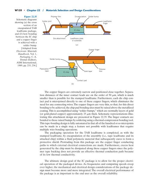
Figure <strong>22</strong>.35<br />
Schematic diagrams<br />
showing (a) the cross<br />
section of an<br />
encapsulated TAB<br />
leadframe package,<br />
<strong>and</strong> (b) how bonding<br />
between the IC chip<br />
<strong>and</strong> a copper finger<br />
is achieved with a<br />
solder bump.<br />
[Adapted from<br />
Electronic <strong>Materials</strong><br />
H<strong>and</strong>book, Vol. 1,<br />
Packaging, C. A.<br />
Dostal (Editor),<br />
ASM International,<br />
1989, pp. 233, 234.]<br />
Solder joint<br />
Passivation<br />
layer<br />
Polymer film Encapsulation Solder bump<br />
Die attachment<br />
Solder bump<br />
IC chip<br />
IC chip<br />
Leadframe plate<br />
or substrate<br />
(b)<br />
(a)<br />
Contact pad<br />
Gold layer<br />
Copper finger<br />
Polymer<br />
film<br />
Leadframe<br />
finger<br />
The copper fingers are extremely narrow <strong>and</strong> positioned close together. Separation<br />
distances of the inner contact leads are on the order of 50 mm,<br />
which is much<br />
smaller than is possible for the stamped leadframe. Furthermore, each die chip contact<br />
pad is microjoined directly to one of these copper fingers, which eliminates the<br />
need for any connecting wires. The copper fingers are very thin, so that, for this direct<br />
bonding to be achieved, the chip pad bonding sites must be raised above the metallized<br />
coating. This is accomplished using “solder bumps,” which are normally layers of gold<br />
(or gold-plated copper) approximately 25 mm<br />
thick. Schematic representations illustrating<br />
this attachment design are presented in Figure <strong>22</strong>.35. The finger contacts are<br />
bonded to these raised bumps by soldering using a thermal-compression bonding tool.<br />
This tape-bonding design is fully automated in that all of the hundred or so microjoints<br />
can be made in a single step, a feature not possible with leadframes that require<br />
multiple wire-bonding operations.<br />
The packaging operation for the TAB leadframe is completed, as with the<br />
stamped leadframe, by encapsulation of the assembly (i.e., tape leadframe <strong>and</strong> its<br />
attached chip) within a fluid polymeric material that subsequently cures to form a<br />
protective shield. Protruding from this package are the copper finger conducting<br />
paths to which external electrical connections are made. Furthermore, excess heat<br />
generated by the chip must be dissipated along these copper fingers since the polymer<br />
tape backing does not provide an effective thermal conduction path because<br />
of its low thermal conductivity.<br />
The ultimate design goal of the IC package is to allow for the proper electrical<br />
operation of the packaged device. As frequencies <strong>and</strong> computing speeds creep<br />
ever higher, the mechanical <strong>and</strong> electrical design considerations of the package design<br />
must become more <strong>and</strong> more integrated. The overall electrical performance of<br />
the package is as important to the end user as the overall reliability.