Chapter 22 Materials Selection and Design Considerations
Chapter 22 Materials Selection and Design Considerations
Chapter 22 Materials Selection and Design Considerations

You also want an ePaper? Increase the reach of your titles
YUMPU automatically turns print PDFs into web optimized ePapers that Google loves.
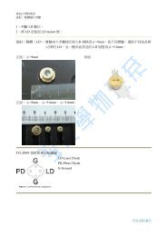
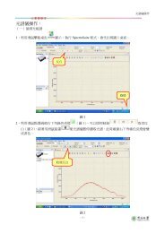
Figure <strong>22</strong>.30<br />
(a) Schematic<br />
diagram showing<br />
the IC chip, its<br />
attachment to the<br />
substrate (or<br />
leadframe plate),<br />
<strong>and</strong> the connecting<br />
wires that run to<br />
the leadframe<br />
contact leads.<br />
(b) Photograph<br />
showing a portion<br />
of a leadframe<br />
package. Included is<br />
the IC chip along<br />
with its connecting<br />
wires. One end of<br />
each wire is bonded<br />
to a chip pad; the<br />
other wire extremity<br />
is bonded to a<br />
leadframe contact<br />
7 1<br />
lead. 2�.<br />
[Figure<br />
(a) adapted from<br />
Electronic <strong>Materials</strong><br />
H<strong>and</strong>book, Vol. 1,<br />
Packaging, C. A.<br />
Dostal, editor, ASM<br />
International, 1989,<br />
p. <strong>22</strong>5. The<br />
photograph in (b)<br />
courtesy of National<br />
Semiconductor<br />
Corporation.]<br />
<strong>22</strong>.17 Die Bonding • W123<br />
electrically conductive path between the chip <strong>and</strong> the leadframe. Curing of the<br />
epoxy is carried out at temperatures between 60�C (140�F) <strong>and</strong> 350�C (660�F) depending<br />
on the application. Since the amounts of thermal expansion are different<br />
for the Cu alloy leadframe plate <strong>and</strong> Si chip, the epoxy adhesive must be capable<br />
of absorbing any thermal strains produced during temperature changes such that<br />
the mechanical integrity of the junction is maintained. Figure <strong>22</strong>.30a shows a<br />
schematic diagram of a chip that is bonded to a substrate layer that is, in turn,<br />
bonded to the leadframe plate. Figure <strong>22</strong>.30b is a photograph of a chip, its leadframe,<br />
<strong>and</strong> the connecting wires.<br />
Leadframe<br />
V<br />
V V<br />
Leadframe plate<br />
Wedge bond<br />
(a)<br />
(b)<br />
Connecting wire<br />
Ball bond<br />
Substrate (optional)<br />
Contact pad<br />
Chip (die)<br />
attachment