Chapter 22 Materials Selection and Design Considerations
Chapter 22 Materials Selection and Design Considerations
Chapter 22 Materials Selection and Design Considerations

Create successful ePaper yourself
Turn your PDF publications into a flip-book with our unique Google optimized e-Paper software.
W120 • <strong>Chapter</strong> <strong>22</strong> / <strong>Materials</strong> <strong>Selection</strong> <strong>and</strong> <strong>Design</strong> <strong>Considerations</strong><br />
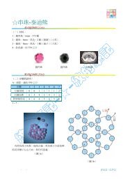
arrayed in the manner shown in the photograph are collectively referred to as dice.<br />
Each IC or die (singular of dice) is first tested for functionality, after which it is removed<br />
from the wafer in a meticulous sawing or “scribe <strong>and</strong> break” operation. Next,<br />
the die is mounted in some type of package. The packaged IC may then be bonded<br />
to a printed circuit board. The purpose of this section is to discuss the material<br />
requirements <strong>and</strong> some of the materials that are used for the various IC package<br />
components.<br />
Some of the functions that an integrated circuit package must perform include<br />
the following:<br />
1. To permit electrical contact between the devices on the chip <strong>and</strong> the<br />
macroscopic world. The contact pads on the surface of the IC are<br />
so minuscule <strong>and</strong> numerous that accommodation of macroscopic wiring<br />
is simply not possible.<br />
2. To dissipate excess heat. While in operation, the many electronic devices<br />
generate significant quantities of heat, which must be dissipated away from<br />
the chip.<br />
3. To protect delicate electrical connections on the chip from chemical degradation<br />
<strong>and</strong> contamination.<br />
4. To provide mechanical support so that the small <strong>and</strong> fragile chip may be<br />
h<strong>and</strong>led.<br />
5. To provide an adequate electrical interface such that the performance of the<br />
IC itself is not significantly degraded by the package design.<br />
Thus, IC packaging also poses a host of material dem<strong>and</strong>s that are very challenging.<br />
In fact, it has been noted that the performance of some ICs is limited, not<br />
by the characteristics of the semiconducting materials or by the metallization<br />
process, but rather by the quality of the package. There are a number of different<br />
package designs used by the various IC manufacturers. For one of the common designs,<br />
the leadframe, we have elected to discuss the various components <strong>and</strong>, for<br />
each component, the materials that are employed along with their property limitations.<br />
This package design is popular with digital IC manufacturers primarily because<br />
its production can be highly automated.<br />
<strong>22</strong>.16 LEADFRAME DESIGN AND MATERIALS<br />
The leadframe, as the name suggests, is a frame to which electrical leads may be<br />
made from the IC chip. A photograph of a leadframe-type package is shown in<br />
Figure <strong>22</strong>.29. In essence, the leadframe consists of a central plate onto which the<br />
die is mounted, <strong>and</strong> an array of contact leads to which wire connections may be<br />
made from the contact pads on the chip. Some leadframe designs also call for a<br />
substrate onto which the die is mounted; this substrate is, in turn, bonded to the<br />
central plate. During the packaging process, <strong>and</strong> after the chip has been attached<br />
to the central plate (a procedure termed die bonding), the contact pads on the IC<br />
chip are cleaned, wires are attached to both the contact pads <strong>and</strong> the leadframe<br />
leads (called wire bonding), <strong>and</strong>, finally, this package is encapsulated in a protective<br />
enclosure to seal out moisture, dust, <strong>and</strong> other contaminants. This procedure<br />
is called hermetic sealing.<br />
There are some rather stringent requirements on the properties of the material<br />
to be used for the leadframe; these are as follows: (1) The leadframe material<br />
must have a high electrical conductivity because there will be current passage<br />
through its leads. (2) The leadframe, the die attach central plate, substrate (if present),