Chapter 22 Materials Selection and Design Considerations
Chapter 22 Materials Selection and Design Considerations
Chapter 22 Materials Selection and Design Considerations

Create successful ePaper yourself
Turn your PDF publications into a flip-book with our unique Google optimized e-Paper software.
<strong>22</strong>.15 Introduction • W119<br />
<strong>and</strong> also with regard to other factors to include material degradability, flexibility,<br />
grip, puncture resistance, etc.<br />
<strong>Materials</strong> for Integrated Circuit Packages<br />
<strong>22</strong>.15 INTRODUCTION<br />
The microelectronic circuitry, including the integrated circuits that are used in our<br />
modern computers, calculators, <strong>and</strong> other electronic devices, was briefly discussed<br />
in Section 18.15. The heart of the integrated circuit (abbreviated IC) is the chip, a<br />
small rectangular substrate of high-purity <strong>and</strong> single-crystal silicon (or more recently<br />
gallium arsenide) onto which literally millions of circuit elements are imprinted.<br />
Circuit elements (i.e., transistors, resistors, diodes, etc.) are created by selectively<br />
adding controlled concentrations of specific impurities to extremely minute <strong>and</strong><br />
localized regions near the surface of the semiconducting material using involved<br />
photolithographic techniques. The chips are small in size, with the largest on the<br />
1<br />
4<br />
order of 6 mm ( in.) on each side <strong>and</strong> approximately 0.4 mm (0.015 in.) thick.<br />
Photographs of a typical chip are shown in Figure 18.27.<br />
Furthermore, chips are very fragile inasmuch as silicon is a relatively brittle material<br />
<strong>and</strong> gallium arsenide is even more brittle. It is also necessary to fabricate conducting<br />
circuit paths over the surface of the chip to facilitate the passage of current<br />
from device to device; on silicon ICs the metal conductor used is aluminum or an aluminum–silicon<br />
alloy (99 wt% Al, 1 wt% Si) that is metallized onto the chip surface to<br />
form a very thin film. The chip design also calls for these circuit paths to terminate at<br />
contact pads on the chip periphery, at which points electrical connections may be made<br />
with the macroscopic world. It should be obvious that a functioning microelectronic<br />
chip is a very sophisticated electronic entity, that materials requirements are very stringent,<br />
<strong>and</strong> that elegant processing techniques are involved in its fabrication.<br />
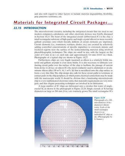
A large number of IC chips are fabricated onto a circular thin wafer of singlecrystal<br />
Si, as shown in the photograph in Figure <strong>22</strong>.28. Single crystals of Si having<br />
diameters as large as 200 mm (8 in.) are routinely grown.The small rectangular ICs<br />
Figure <strong>22</strong>.28<br />
Photograph of a 100mm-diameter(4-in.diameter)<br />
silicon<br />
wafer. Each of the<br />
small rectangles<br />
shown is an<br />
individual IC chip or<br />
die. (Photography by<br />
S. Tanner.)