Electronic Devices & Circuits - KEI
Electronic Devices & Circuits - KEI
Electronic Devices & Circuits - KEI

You also want an ePaper? Increase the reach of your titles
YUMPU automatically turns print PDFs into web optimized ePapers that Google loves.
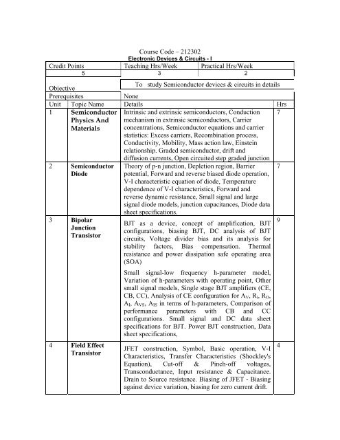
Course Code – 212302<br />
<strong>Electronic</strong> <strong>Devices</strong> & <strong>Circuits</strong> - I<br />
Credit Points Teaching Hrs/Week Practical Hrs/Week<br />
5 3 2<br />
Objective<br />
To study Semiconductor devices & circuits in details<br />
Prerequisites<br />
None<br />
Unit Topic Name Details Hrs<br />
1 Semiconductor<br />
Physics And<br />
Materials<br />
Intrinsic and extrinsic semiconductors, Conduction<br />
mechanism in extrinsic semiconductors, Carrier<br />
concentrations, Semiconductor equations and carrier<br />
statistics: Excess carriers, Recombination process,<br />
Conductivity, Mobility, Mass action law, Einstein<br />
relationship. Graded semiconductor, drift and<br />
7<br />
2 Semiconductor<br />
Diode<br />
3 Bipolar<br />
Junction<br />
Transistor<br />
4 Field Effect<br />
Transistor<br />
diffusion currents, Open circuited step graded junction<br />
Theory of p-n junction, Depletion region, Barrier<br />
potential, Forward and reverse biased diode operation,<br />
V-I characteristic equation of diode, Temperature<br />
dependence of V-I characteristics, Forward and<br />
reverse dynamic resistance, Small signal and large<br />
signal diode models, junction capacitances, Diode data<br />
sheet specifications.<br />
BJT as a device, concept of amplification, BJT<br />
configurations, biasing BJT, DC analysis of BJT<br />
circuits, Voltage divider bias and its analysis for<br />
stability factors, Bias compensation. Thermal<br />
resistance and power dissipation safe operating area<br />
(SOA)<br />
Small signal-low frequency h-parameter model,<br />
Variation of h-parameters with operating point, Other<br />
small signal models, Single stage BJT amplifiers (CE,<br />
CB, CC), Analysis of CE configuration for A V , R i , R O ,<br />
A I , A VS , A IS in terms of h-parameters, Comparison of<br />
performance parameters with CB and CC<br />
configurations. Small signal and DC data sheet<br />
specifications for BJT. Power BJT construction, Data<br />
sheet specifications,<br />
JFET construction, Symbol, Basic operation, V-I<br />
Characteristics, Transfer Characteristics (Shockley's<br />
Equation), Cut-off & Pinch-off voltages,<br />
Transconductance, Input resistance & Capacitance.<br />
Drain to Source resistance. Biasing of JFET - Biasing<br />
against device variation, biasing for zero current drift.<br />
7<br />
9<br />
4
5 MOSFET<br />
6 Frequency<br />
Response of<br />
Amplifiers<br />
MIS structures, two terminal structure:<br />
MOS capacitor, concept of accumulation, depletion<br />
and inversion; four terminal structure: MOSFET, its I-<br />
V characteristics, drain current equation in terms of<br />
W/L, second order effects, brief introduction to MOS<br />
scaling and scaling issues viz. short channel effects.<br />
Power MOSFET Construction, Comparison with power<br />
BJT<br />
Concept of frequency response, Human ear response<br />
to audio frequencies, significance of Octaves and<br />
Decades. The decibel unit. Square wave testing of<br />
amplifiers, Miller's theorem. Effect of coupling,<br />
bypass, junction and stray capacitances on frequency<br />
response for BJT and FET amplifiers. Concept of<br />
dominant pole.<br />
9<br />
5<br />
Lab/ Term Work<br />
1. Study of JFET drain and transfer characteristics.<br />
2. JFET biasing arrangement Graphical method.<br />
3. Build and Test JFET CS amplifier.<br />
Find performance parameters for JFET amplifier - A V , R i , R O .<br />
4. Simulation of JFET CS amplifier using multisim/spice.<br />
Find performance parameters for JFET amplifier - A V , R i , R O and compare with<br />
theoretical and practical results.<br />
5. Input and Output Characteristics of BJT CE configuration. Find h parameters from<br />
characteristics.<br />
6. Build and Test BJT in CE amplifier and find performance parameters - A V , R i , R O , A I<br />
7. Simulation of BJT CE amplifier using multisim/spice<br />
Find performance parameters for BJT amplifier - A V , R i , R O , A I and compare with<br />
theoretical and practical results.<br />
8. Comparison of CE, CC, CB configurations in terms of A V , R i , R O , A I .<br />
9. Study of MOSFET drain and transfer characteristics<br />
10. Frequency response - For BJT/ FET single stage amplifiers - Effect of unbypassed<br />
R E and R S . Effect of coupling and bypass capacitors on low frequency cut-off.<br />
Text Books<br />
Reference Books<br />
1. Millman Halkias, <strong>Electronic</strong> Device & <strong>Circuits</strong>, Tata<br />
McGraw Hill<br />
2. Thomas L. Floyd, <strong>Electronic</strong> <strong>Devices</strong>, Pearson Education<br />
1. B.G. Streetman, Solid State <strong>Electronic</strong> <strong>Devices</strong>, Prentice Hall<br />
of India, New Delhi.<br />
2. Millman Halkias, Integrated <strong>Electronic</strong>s, Tata McGraw Hill<br />
3. Millman Grabel, Microelectronics, Tata McGraw Hill<br />
4. Thomas L. Floyd, <strong>Electronic</strong> <strong>Devices</strong>, Pearson Education
Related Websites<br />
www.digikey.com<br />
For component selection and datasheets<br />
Examination Scheme<br />
Internal Assessment – 40 marks<br />
Term Work – 25 marks<br />
Final Theory Paper – 60 marks