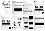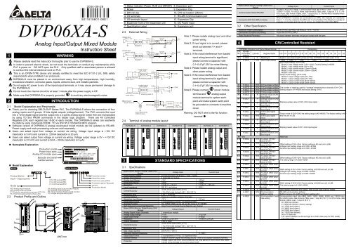
DVP06XA-S
DVP06XA-S
DVP06XA-S

Create successful ePaper yourself
Turn your PDF publications into a flip-book with our unique Google optimized e-Paper software.
http://www.delta.com.tw/products/plc.asp<br />
<strong>DVP06XA</strong>-S<br />
Analog Input/Output Mixed Module<br />
Instruction Sheet<br />
1 WARNING<br />
Please carefully read this instruction thoroughly prior to use the <strong>DVP06XA</strong>-S.<br />
In order to prevent electric shock, do not touch the terminals or conduct any maintenance while<br />
PLC is power on. DO NOT open the PLC. Only qualified staff or associated person is allowed<br />
to conduct the internal electrical work on PLC.<br />
This is an OPEN-TYPE device and already certified to meet the IEC 61131-2 (UL 508) safety<br />
requirements when installed in an enclosure.<br />
<strong>DVP06XA</strong>-S must be placed in an environment away from high temperatures, high humidity,<br />
exceessive vibration, corrosive gases, liquids, airborne dust, and metallic particles.<br />
Do not apply AC power to any of the input/output terminals, or it may cause permanent damage to<br />
the <strong>DVP06XA</strong>-S.<br />
Do not touch the internal circuit for at least 1 minute after the power supply is Off.<br />
Make sure that <strong>DVP06XA</strong>-S is properly grounded<br />
2 INTRODUCTION<br />
, to avoid any electromagnetic noise.<br />
2.1 Model Explanation and Peripherals<br />
• Thank you for choosing DELTA DVP Series PLC. The <strong>DVP06XA</strong>-S allows the connection of four<br />
analog inputs and 2 groups 12 bits digital outputs (voltage/current). The PLC converts the input<br />
into a 12-bit digital signal and the output into a 2 points analog signal, which then are manipulated<br />
by using TO and FROM commands in the ladder logic program. There are 49 Controlled<br />
Registers (CR, each register has 16-bit) in each module. The <strong>DVP06XA</strong>-S series can read/write<br />
the data by using commands FROM / TO via DVP-PLC SS/SA/SX MPU program.<br />
• Software version of <strong>DVP06XA</strong>-S analog input/output mixed module can be updated via RS-485.<br />
Power supply and main processing units are sold separately.<br />
• Users can select input from voltage or current via wiring. Voltage input range is ±10V DC<br />
(resolution is 5 mV) and current is ±20mA (resolution is 20 µA).<br />
• Users can select output from voltage or current via wiring. Voltage output range is 0V ~ +10V DC<br />
(resolution is 2.5 mV) and current is 0mA ~ 20mA (resolution is 5 µA).<br />
• Nameplate Explanation<br />
• Model Explanation<br />
Model<br />
Product Series<br />
Input + Output points<br />
Model type<br />
Production model<br />
Power input spec.<br />
Analog I/O module spec.<br />
Barcode and serial<br />
number version<br />
AD: Analog input module<br />
DA: Analog output module<br />
PT: Platinum temperature sensors (PT-100)<br />
TC: Thermocouple sensors (Type J/K)<br />
2.2 Product Profile and Outline<br />
2<br />
3<br />
1<br />
90.00<br />
3.00 25.20<br />
4.00<br />
IN<br />
V+<br />
C<br />
I+ H<br />
1<br />
COM<br />
V+<br />
C<br />
I+ H<br />
2<br />
COM<br />
V+<br />
C<br />
I+ H<br />
3<br />
COM<br />
V+<br />
C<br />
I+ H<br />
4<br />
COM<br />
V+<br />
C<br />
I+ H<br />
5<br />
COM<br />
V+<br />
C<br />
I+ H<br />
6<br />
COM<br />
OUT<br />
4<br />
5<br />
60.00<br />
VX.X<br />
S: for SS series MPU<br />
P: for EP series MPU<br />
H: for EH series MPU<br />
Serial Number<br />
XA: Analog input/output mixed module<br />
RT: Resistor Thermocouple<br />
HC: Input module of high-speed counter<br />
PU: single axis positioning unit<br />
6<br />
7<br />
8<br />
10<br />
9<br />
3<br />
UNIT:mm<br />
20.4VDC ~ 26.4VDC<br />
- 10V ~ + 10V or - 20mA ~ + 20mA<br />
/ 0V ~ + 10V or 0mA ~ +20mA<br />
5mV or 20 A / 2.5mV or 5 A<br />
06XA-S0T325003<br />
MADE IN XXXXXX<br />
3.00<br />
11<br />
13<br />
12<br />
14<br />
3.4<br />
Production series<br />
Production week<br />
Production year (2004)<br />
Production place (Taoyuan)<br />
Version<br />
Production Model<br />
60.00<br />
90.00<br />
1. Status indicator (Power, RUN and ERROR) 8. Expansion port<br />
2. Model 9. Expansion Clip<br />
3. DIN rail clip 10. DIN rail location (35mm)<br />
4. I/O terminals 11. RS-485 Communication port<br />
5. I/O terminals layout 12. Expansion Clip<br />
6. Expansion hole of the expansion unit 13. DC Power input<br />
7. Specification Label 14. Expansion port<br />
2.3 External Wiring<br />
Voltage input<br />
-10V~+10V<br />
Current input<br />
-20mA~+20mA<br />
Shielded*1<br />
*5<br />
AC drive, recorder,<br />
scale valve...<br />
Shielded*1<br />
AC drive, recorder,<br />
scale valve...<br />
terminal of<br />
power module<br />
CH1<br />
V+<br />
*3 I+<br />
COM<br />
CH4<br />
*2<br />
voltage output<br />
V+<br />
I+<br />
COM<br />
0V~+10V<br />
CH5<br />
V+<br />
I+<br />
COM<br />
shielding cable *1<br />
current output<br />
0mA~20mA<br />
shielding cable *4<br />
class 3 grounding<br />
(100 or less)<br />
DC24V<br />
104.7K<br />
250<br />
104.7K<br />
AG<br />
104.7K<br />
250<br />
104.7K<br />
CH6<br />
V+<br />
I+<br />
COM<br />
24+<br />
24-<br />
2.4 Terminal of analog module layout<br />
AG<br />
DC/DC<br />
converter<br />
CH5<br />
CH6<br />
CH1<br />
CH4<br />
+15V<br />
AG<br />
-15V<br />
Note 1: Please isolate analog input and other<br />
power wiring.<br />
Note 2: If input signal is in current, please<br />
short out between V+ and I+<br />
terminals.<br />
Note 3: If the noise interference from loaded<br />
input wiring terminal is significant,<br />
please connect a capacitor with<br />
0.1~0.47µF 25V for noise filtering.<br />
Note 4: Please isolate analog output and<br />
other power wiring.<br />
Note 5: If the noise interference from loaded<br />
input wiring terminal is significant,<br />
please connect a capacitor with<br />
0.1~0.47µF 25V for noise filtering.<br />
Note 6: Please connect power module<br />
terminal and analog output<br />
module terminal to system earth<br />
point and make system earth point<br />
be grounded or connects to machine<br />
cover.<br />
Warning: DO NOT wire to the No function<br />
terminal<br />
DVP04AD-S DVP02DA-S DVP04DA-S DVP04PT-S DVP04TC-S <strong>DVP06XA</strong>-S DVP08RT-S<br />
V+<br />
I+<br />
COM<br />
FG<br />
V+<br />
I+<br />
COM<br />
FG<br />
V+<br />
I+<br />
COM<br />
FG<br />
V+<br />
I+<br />
COM<br />
FG<br />
V+<br />
I+<br />
COM<br />
FG<br />
V+<br />
I+<br />
COM<br />
FG<br />
V+<br />
I+<br />
COM<br />
FG<br />
V+<br />
I+<br />
COM<br />
FG<br />
V+<br />
I+<br />
COM<br />
FG<br />
V+<br />
I+<br />
COM<br />
FG<br />
3 STANDARD SPECIFICATIONS<br />
3.1 Specifications<br />
Mixed (06XA) Module, Analog/ Digital (A/D)<br />
Module<br />
Voltage Input<br />
Current Input<br />
Power Supply Voltage 24 VDC(20.4VDC~28.8VDC) ( –15%〜+20%)<br />
Analog Input Channel<br />
4 channels per module<br />
Analog Input Range ±10V ±20mA<br />
Digital Data Range ±2000 ±1000<br />
Resolution 12 bits (1 LSB =5 mV) 11 bits (1 LSB =20 µA)<br />
Input Impedance 200 KΩ and above 250Ω<br />
Overall Accuracy<br />
±0.5% of full scale of 25℃(77℉)<br />
±1% of full scale during 0~55℃ (32~131℉)<br />
Response Time<br />
3 ms × channels<br />
Isolation Method<br />
There is no isolation between channels.<br />
Absolution Input Range ±15 V ±32 mA<br />
Digital Data Format<br />
2’s complement of 16-bit, (13 Significant Bits)<br />
Average Function<br />
Yes (CR#2~CR#5 can be set and the range is K1~K4096)<br />
Self diagnostic function Self Detection Upper bound and lower bound detection per channel<br />
Mixed (06XA) Module, Digital/Analog (D/A)<br />
Module<br />
Voltage Output<br />
Current Output<br />
Analog Signal Output Channels<br />
2 channel per module<br />
Analog Output Range 0~10V 0~20 mA<br />
Digital Data Range 0~4000 0~4000<br />
Resolution 12 bits (1 LSB =2.5 mV) 12 bits (1 LSB =5 µA)<br />
Output Impedance<br />
0.5Ω or lower<br />
Overall Accuracy<br />
±0.5% of full scale of 25℃(77℉)<br />
±1% of full scale during 0~55℃ (32~131℉)<br />
Response Time<br />
3 ms ×Channels<br />
Max. Output Current 20mA (1KΩ~2MΩ) -<br />
Tolerance Carried Impedance - 0〜500Ω<br />
Digital Data Format<br />
2’s complement of 16-bit, (13 Significant Bits)<br />
Isolation Method<br />
Isolation between digital and analog circuitry. There is no isolation between channels.<br />
Protection<br />
Voltage output has short circuit protection but long period of short circuit may cause<br />
internal wiring damage and current output break.<br />
L+<br />
L-<br />
I-<br />
FG<br />
L+<br />
L-<br />
I-<br />
FG<br />
L+<br />
L-<br />
I-<br />
FG<br />
L+<br />
L-<br />
I-<br />
FG<br />
L+<br />
L-<br />
SLG<br />
L+<br />
L-<br />
SLG<br />
L+<br />
L-<br />
SLG<br />
L+<br />
L-<br />
SLG<br />
V+<br />
I+<br />
COM<br />
V+<br />
I+<br />
COM<br />
V+<br />
I+<br />
COM<br />
V+<br />
I+<br />
COM<br />
V+<br />
I+<br />
COM<br />
V+<br />
I+<br />
COM<br />
L+<br />
L-<br />
L+<br />
L-<br />
L+<br />
L-<br />
L+<br />
L-<br />
L+<br />
L-<br />
L+<br />
L-<br />
L+<br />
L-<br />
L+<br />
L-<br />
Mixed (06XA) Module, Analog/ Digital (A/D)<br />
Module<br />
Communication Mode (RS-485)<br />
Connect to DVP-PLC MPU in Series<br />
3.2 Other Specification<br />
Voltage Input<br />
Current Input<br />
MODBUS ASCII/RTU Mode. Communication baud rate of 4800 / 9600 / 19200 / 38400<br />
/ 57600 / 115200. For ASCII mode, date format is 7Bits, even, 1 stop bit (7 E 1). For<br />
RTU mode, date format is 8Bits, even, 1 stop bit (8 E 1). The RS-485 is disabled when<br />
the <strong>DVP06XA</strong>-S is connected in series with MPU.<br />
When <strong>DVP06XA</strong>-S modules are connected to an MPU, the modules are numbered<br />
from 0 - 7. 0 is the closest to the MPU and 7 is the furthest. The Maximum number of<br />
modules is 8 modules and they do not occupy any digital I/O points of the MPU.<br />
Maximum Power Consumption 2W at 24 VDC (20.4VDC~28.8VDC) ( -15 % ~ +20 %)<br />
Environment Condition and Wiring<br />
Follow the DVP-PLC MPU.<br />
Static Electricity Prevention<br />
All places between terminals and ground comply with the spec.<br />
4 CR(Controlled Register)<br />
<strong>DVP06XA</strong>-S Analog Input/Output Mixed Module<br />
Explanation<br />
CR<br />
No<br />
RS-485<br />
Parameter Latched Register Name b15 b14 b13 b12 b11 b10 b9 b8 b7 b6 b5 b4 b3 b2 b1 b0<br />
Address<br />
#0 H 40C8 ○ R Model type System used, data length is 8 bits (b7~b0). <strong>DVP06XA</strong>-S model code= H CC<br />
#1 H 40C9 ○ R/W Input mode setting CH6 CH5 CH4 CH3 CH2 CH1<br />
Input mode setting: (CH1~CH4)<br />
Mode 0: input voltage mode (-10V~+10V). Factory Setting is H0000.<br />
Mode 1: input voltage mode (-6V~+10V).<br />
Mode 2: input current mode (-12mA~+20mA).<br />
Mode 3: input current mode (-20mA~+20mA).<br />
Mode 4: none use.<br />
Output mode setting: (CH5~CH6)<br />
Mode 0: output voltage mode (0V~10V).<br />
Mode 1: output voltage mode (2V~10V).<br />
Mode 2: output current mode (4mA~20mA).<br />
Mode 3: output current mode (0mA~20mA).<br />
#2 H 40CA ○ R/W CH1 average number<br />
#3 H 40CB ○ R/W CH2 average number<br />
#4 H 40CC ○ R/W CH3 average number<br />
#5 H 40CD ○ R/W CH4 average number<br />
#6 H 40CE ╳ R average value of CH1<br />
input signal<br />
#7 H 40CF ╳ R average value of CH2<br />
input signal<br />
#8 H 40D0 ╳ R average value of CH3<br />
input signal<br />
#9 H 40D1 ╳ R average value of CH4<br />
input signal<br />
#10 H 40D2 ╳ R/W CH5 output signal<br />
value<br />
#11 H 40D3 ╳ R/W CH6 output signal<br />
value<br />
#12 H 40D4 ╳ R present value of CH1<br />
input signal<br />
#13 H 40D5 ╳ R present value of CH2<br />
input signal<br />
#14 H 40D6 ╳ R present value of CH3<br />
input signal<br />
#15 H 40D7 ╳ R present value of CH4<br />
input signal<br />
#16~ #17 Reserved<br />
#18 H 40DA ○ R/W To adjust OFFSET<br />
value of CH1<br />
#19 H 40DB ○ R/W To adjust OFFSET<br />
value of CH2<br />
#20 H 40DC ○ R/W To adjust OFFSET<br />
value of CH3<br />
#21 H 40DD ○ R/W To adjust OFFSET<br />
value of CH4<br />
#22 H 40DE ○ R/W To adjust OFFSET<br />
value of CH5<br />
#23 H 40DF ○ R/W To adjust OFFSET<br />
value of CH6<br />
#24 H 40E0 ○ R/W To adjust GAIN value<br />
of CH1<br />
#25 H 40E1 ○ R/W To adjust GAIN value<br />
of CH2<br />
#26 H 40E2 ○ R/W To adjust GAIN value<br />
of CH3<br />
#27 H 40E3 ○ R/W To adjust GAIN value<br />
of CH4<br />
#28 H 40E4 ○ R/W To adjust GAIN value<br />
of CH5<br />
#29 H 40E5 ○ R/W To adjust GAIN value<br />
of CH6<br />
The number of readings used for “average” temperature on channels CH1~CH4.<br />
Setting range is K1~K4096 and factory setting is K10.<br />
Display average value of CH1~CH4 input signal<br />
Output value of CH5~CH6, the setting range is K0~K4000. The factory setting is K0<br />
and the unit is LSB.<br />
Display present value of CH1~CH4 input signal<br />
Offset setting of CH1~CH4. Factory setting is K0 and unit is LSB.<br />
Voltage input: setting range is K-1000 ~K1000<br />
Current input: setting range is K-1000 ~K1000<br />
Offset setting of CH5~CH6. Factory setting is K0 and unit is LSB.<br />
The setting range is K-2000~K2000<br />
GAIN setting of CH1~CH4. Factory setting is K1000 and unit is LSB.<br />
Voltage input: setting range is K-800 ~K4000<br />
Current input: setting range is K-800 ~K2600<br />
GAIN setting of CH5~CH6. Factory setting is K2000 and unit is LSB.<br />
The setting range is K-1600~K8000<br />
#30 H 40E6 ╳ R Error status Data register stores the error status, refer to fault code chart for details.<br />
#31 H 40E7 ○ R/W Communication<br />
address setting<br />
RS-485 communication address.<br />
Setting range is K1~K255 and factory setting is K1<br />
#32 H 40E8 ○ R/W Communication baud Communication baud rate (4800, 9600, 19200, 38400, 57600 and 115200 bps).<br />
rate setting<br />
For ASCII mode, date format is 7Bits, even, 1 stop bit (7 E 1). For RTU mode, date<br />
format is 8Bits, even, 1 stop bit (8 E 1).<br />
b0: 4800 bps (bit/sec)<br />
b1: 9600 bps (bit/sec). (factory setting)<br />
b2: 19200 bps (bit/sec).<br />
b3: 38400 bps (bit/sec).<br />
b4: 57600 bps (bit/sec).<br />
b5: 115200 bps (bit/sec).<br />
b6~b13: Reserved.<br />
b14: switch between low bit and high bit of CRC code (only for RTU mode)<br />
b15: RTU mode.
#33 H 40E9 ○ R/W Reset to factory b15 b14 b13 b12 b11 b10 b9 b8 b7 b6 b5 b4 b3 b2 b1 b0<br />
setting and set CH6 CH5 CH4 CH3 CH2 CH1<br />
characteristics<br />
adjustable priority<br />
Example: Setting of CH1<br />
1. When b0=0, user can set OFFSET and GAIN value of CH1 (CR#18, CR#24).<br />
When b0=1, inhibit user to adjust OFFSET and GAIN value of CH1 (CR#18,<br />
CR#24).<br />
2. b1 means if characteristic register is latched. b1=0 (factory setting, latched), b1=1<br />
(not latched).<br />
3. b2: Set to 1 and PLC will be reset to factory settings.<br />
The setting of CH5~CH6, give CH5 setting for example:<br />
b13, b12:<br />
00: can be adjusted, latched.<br />
01: can be adjusted, non-latched.<br />
10: inhibit adjust.<br />
11: reset to factory settings and clear b12, b13 to 0.<br />
#34 H 40EA ○ R Software version Display software version in hexadecimal. Example: H 010A = version 1.0A.<br />
#35~#48 System used<br />
○ means latched.<br />
╳ means non-latched.<br />
R means can read data by using FROM command or RS-485.<br />
W means can write data by using TO command or RS-485.<br />
LSB (Least Significant Bit): 1. Voltage input: 1 LSB =10V/2000=5mV. 2. Current input: 1 LSB =20mA/1000=20µA.<br />
3. Voltage output: 1 LSB =10V/4000=2.5mV. 4. Current output: 1 LSB =20mA/4000=5µA.<br />
Explanation:<br />
1. CR#0: The PLC model type.<br />
2. CR#1: b11~b0 are used to set 4 internal channels working mode of analog input module (AD).<br />
b12~b15 are used to set 2 channels working mode of analog output module (DA). Every channel<br />
has four modes that can be set individually. For example: if setting CH1 to mode 0 (b2~b0=000),<br />
CH2 to mode 1(b5~b3=001), CH3: mode2 (b8~b6=010), CH4: mode 3(b11~b9=011), b0~b11<br />
need be set to H688. If setting CH5: mode 2 (b13~b12=10), CH6: mode 1 (b15~b14=01),<br />
b12~b15 need be set to H5. The factory setting is H0000.<br />
3. CR#2 ~ CR#5: Used to set the number of piece of input readings for the average temperature<br />
calculation. The available range is K1~K4096 and factory setting is K10.<br />
4. CR#6 to CR#9: The average value of temperature in ℃. Temperature is calculated by averaging<br />
multiple temperature readings. Example: If CR#2 is 10, the temperature in CR#6 will be the<br />
average of the last 10 readings on CH1.<br />
5. CR#10 ~ CR#11 are used to set the output value of CH5 and CH6. The setting range is<br />
K0~K4000. The factory setting is K0 and unit is LSB.<br />
6. CR#12 ~ CR#15: used to save the present value of input signal of CH1~CH4.<br />
7. CR#16, CR#17, CR#28, CR#29 are reserved.<br />
8. CR #18~ CR #21: used to adjust the OFFSET value of CH1~CH4 if analog input either in voltage<br />
or in current is 0 after it converts from analog to digital. Voltage setting range:<br />
-5V~+5V(-1000 LSB ~+1000 LSB ). Current setting range: -20mA~+20mA (-1000 LSB ~+1000 LSB ).<br />
9. CR #22~ CR #23: used to adjust the OFFSET value of CH5~CH6 if analog input either in voltage<br />
or in current is 0 after it converts to digital. Factory setting is K0, and the unit is LSB . The setting<br />
range is -2000~+2000. Voltage setting range: -5V~+5V(-2000 LSB ~+2000 LSB ). Current setting<br />
range: -10mA~+10mA (-2000 LSB ~+2000 LSB ).<br />
10. CR #24~ CR #27: used to adjust the GAIN value of CH1~CH4. The value of analog input either<br />
in voltage or in current after it was converted to digital based upon full scale of 4000. Voltage<br />
setting range: -4V~+20V(-800 LSB ~+4000 LSB ). Current setting range: -16mA~+52mA (-800 LSB<br />
~+2600 LSB ). But it needs to notice that GAIN VALUE - OFFSET VALUE = +200 LSB ~+3000 LSB<br />
(voltage) or +200 LSB ~+1600 LSB (current). If the value difference comes up small (within range),<br />
the output signal resolution is then slim and the variation is definitely larger. On the contrast, if<br />
the value difference exceeds the range, the output signal resolution becomes larger and the<br />
variation is definitely smaller.<br />
11. CR #28~ CR #29: used to adjust the GAIN value of CH5~CH6. The value of analog input either<br />
in voltage or in current after it converts to digital based upon full scale of 2000. Voltage setting<br />
range: -4V~+20V(-1600 LSB ~+8000 LSB ). Current setting range: -8mA ~+40mA (-1600 LSB ~+8000 LSB ).<br />
Please be noticed that GAIN VALUE – OFFSET VALUE = +400 LSB ~+6000 LSB (voltage or current).<br />
If the value difference comes up small (within range), the output signal resolution is then slim<br />
and the variation is definitely larger. On the contrast, if the value difference exceeds the range,<br />
the output signal resolution becomes larger and the variation is definitely smaller.<br />
12. CR#30 is the fault code. Please refer to the chart below.<br />
Fault description Content b15~b8 B7 b6 b5 b4 b3 b2 b1 b0<br />
Power source abnormal K1(H1) 0 0 0 0 0 0 0 1<br />
(Low voltage alarm)<br />
User setting D/A output K2(H2) 0 0 0 0 0 0 1 0<br />
exceeds range<br />
Setting mode error K4(H4) 0 0 0 0 0 1 0 0<br />
Reserved<br />
Offset/Gain error K8(H8) 0 0 0 0 1 0 0 0<br />
Hardware malfunction K16(H10) 0 0 0 1 0 0 0 0<br />
Digital range error K32(H20) 0 0 1 0 0 0 0 0<br />
Average times setting error K64(H40) 0 1 0 0 0 0 0 0<br />
Command error<br />
K128(H80)<br />
1 0 0 0 0 0 0 0<br />
Note: Each fault code will have corresponding bit (b0~b7). Two or more faults may happen at the same time. 0 means<br />
normal and 1 means having fault.<br />
13. CR#31: RS-485 communication address. Setting range is 01~255 and factory setting is K1.<br />
14. CR#32: RS-485 communication baud rate: 4800, 9600, 19200, 38400, 57600 and 115200.<br />
b0:4800bps, b1:9600bps (factory setting), b2:19200bps, b3:38400 bps, b4:57600 bps,<br />
b5:115200 bps, b6~b13: Reserved, b14: switch between low bit and high bit of CRC code (RTU<br />
mode only) b15: ASCII / RTU mode. For ASCII mode, date format is 7Bits, even, 1 stop bit (7 E<br />
1). For RTU mode, date format is 8Bits, even, 1 stop bit (8 E 1).<br />
15. CR#33 is used to set the internal function priority. For example: characteristic register. Output<br />
latched function will save output setting in the internal memory before power loss.<br />
16. CR#34: software version.<br />
17. CR#35~ CR#48: system used.<br />
18. The corresponding parameters address H 40C8~H 40F9 of CR#0~CR#48 will allow user to<br />
read/write data via RS-485.<br />
A. Baud rate can be 4800, 9600, 19200, 38400, 57600, 115200bps.<br />
B. MODBUS communication protocol can be either in ASCII or in RTU mode. For ASCII mode,<br />
date format is 7Bits, even, 1 stop bit (7 E 1). For RTU mode, date format is 8Bits, even, 1<br />
stop bit (8 E 1).<br />
C. Function code: 03H read data from register.<br />
06H write one WORD into register.<br />
10H write multiple WORD into register.<br />
5 Adjust A/D Conversion Characteristic Curve<br />
5.1 Adjust A/D Conversion Characteristic Curve of CH1~CH4<br />
Voltage input mode<br />
-10V -6V<br />
digital output<br />
+2000<br />
Mode 0<br />
+1000<br />
0<br />
2V 5V 6V<br />
OFFSET GAIN<br />
-1000<br />
-2000<br />
Current input mode:<br />
-20mA -12mA<br />
Mode 1<br />
10V<br />
Digital output<br />
Mode 3<br />
+2000<br />
0<br />
4mA<br />
OFFSET<br />
Voltage<br />
input<br />
Mode 2<br />
Current<br />
Input<br />
20mA<br />
GAIN<br />
Mode 0 of CR#1: GAIN=5V(1000 LSB ), OFFSET=0V (0 LSB ).<br />
Mode 1 of CR#1: GAIN=6V(1200 LSB ), OFFSET=2V (400 LSB ).<br />
GAIN: Voltage input value when digital output is 4000.<br />
Setting range is -4V~+20V(-800 LSB ~ +4000 LSB )<br />
OFFSET: Voltage input value when digital output is 0.<br />
Setting range: -5V~+5V(-1000 LSB ~ +1000 LSB )<br />
GAIN-OFFSET: Setting range is +1V~+15V (+200 LSB ~ +3000 LSB )<br />
Mode 2 of CR#1: GAIN = 20mA(1000 LSB ), OFFSET=4mA (200 LSB ).<br />
Mode 3 of CR#1: GAIN = 20mA(1000 LSB ), OFFSET=0mA (0 LSB ).<br />
GAIN: Current input value when digital output is +4000.<br />
Setting range is -20 mA~+20mA (-1000 LSB ~<br />
+1000 LSB )<br />
OFFSET:<br />
Current input value when digital output value is<br />
0. Setting range is-16mA ~+52mA (-800 LSB ~<br />
+2600 LSB )<br />
-2000<br />
GAIN-OFFSET: Setting range is +4mA ~ +32mA (200 LSB ~<br />
+1600 LSB )<br />
Use the chart above to adjust A/D conversion characteristic curve of voltage input mode and current<br />
input mode. Users can adjust conversion characteristic curve by changing OFFSET values<br />
(CR#18~CR#21) and GAIN values (CR#24~CR#27) depend on application.<br />
LSB (Least Significant Bit): 1. voltage input: 1 LSB =10V/2000=5mV. 2. current input: 1 LSB =20mA/1000=<br />
20µA.<br />
5.2 Adjust D/A Conversion Characteristic Curve of CH5~CH6<br />
Voltage output mode<br />
Voltage output<br />
10V<br />
6V<br />
5V<br />
GAIN<br />
mode 1<br />
mode 0<br />
2V<br />
Digital<br />
0 +2000 +4000 input<br />
OFFSET<br />
Current output mode:<br />
Current output<br />
20mA<br />
12mA<br />
10mA<br />
4mA<br />
0<br />
GAIN<br />
OFFSET<br />
Mode 2<br />
Mode 3<br />
Digital<br />
input<br />
+2000 +4000<br />
Mode 0 of CR#1: GAIN = 5V(2000 LSB ), OFFSET=0V (0 LSB )<br />
Mode 1 of CR#1: GAIN = 6V(2400 LSB ), OFFSET=2V (800 LSB ).<br />
GAIN: Voltage output value when digital input is K2000.<br />
Setting range is -4V~+20V(-1600 LSB ~+8000 LSB ).<br />
OFFSET: Voltage output value when digital input is K0.<br />
Setting range: -5V~+5V(-2000 LSB ~ +2000 LSB ).<br />
GAIN-OFFSET: Setting range is +1V~+15V(+400 LSB ~ +6000 LSB )<br />
Mode 2 of CR#1: GAIN = 12mA(2400 LSB ),OFFSET=4mA (800 LSB ).<br />
Mode 3 of CR#1: GAIN = 10mA(2000 LSB ), OFFSET=0mA (0 LSB ).<br />
GAIN:<br />
Current output value when digital input value is<br />
K2000. Setting range is -8mA ~+40mA (-1600 LSB<br />
~+8000 LSB ).<br />
OFFSET: Current output value when digital input is K0.<br />
Setting range is -10mA ~+10mA (-2000 LSB<br />
~+2000 LSB ).<br />
GAIN-OFFSET: Setting range is +2mA~+30mA (+400 LSB<br />
~+6000 LSB )<br />
Use the chart above to adjust D/A conversion characteristic curve of voltage output mode and<br />
current output mode. Users can adjust conversion characteristic curve by changing OFFSET values<br />
(CR#14~CR#15) and GAIN values (CR#18~CR#19) depend on application.<br />
LSB (Least Significant Bit): 1. voltage output: 1 LSB =10V/4000=2.5mV.<br />
2. current output: 1 LSB =20mA/4000=5µA.<br />
5.3 Program Example for Adjusting A/D Conversion Characteristics Curve<br />
Example: setting OFFSET value of CH1 to 0V(=K0 LSB ) and GAIN value of CH1 to 2.5V(=K500 LSB ).<br />
M1002<br />
X0<br />
TO<br />
TO<br />
TO<br />
TO<br />
K0<br />
K0<br />
K0<br />
K0<br />
• Write H0 to CR#1 of analog input module<br />
no. 0 and set CH1 to mode 0 (voltage input<br />
-10V~+10V)<br />
• Write H0 to CR#33 and allow to adjust<br />
characters of CH1.<br />
• When X0 switches from Off to On, K0 LSB of<br />
OFFSET value will be wrote in CR#18 and<br />
K500 LSB of GAIN value will be wrote in<br />
CR#24.<br />
5.4 Program Example for Adjusting D/A Conversion Characteristics Curve<br />
Example: set OFFSET value of CH5 to 0V(=K0 LSB ) and GAIN value of CH1 to 2.5V(=K1000 LSB ).<br />
M1002<br />
X0<br />
TO<br />
TO<br />
TO<br />
TO<br />
K0<br />
K0<br />
K0<br />
K0<br />
6 Initial PLC Start-up<br />
• Write H3000 into CR#1 (b12~b15) of<br />
analog input/output module#0. Setting CH5<br />
to mode 3 (current output 0mA~ +20mA).<br />
• Write H0 into CR#33 (b12~b15) and allow<br />
CH5, CH6 to adjust characteristics.<br />
• When X0 switches from Off to On, K0 LSB of<br />
OFFSET value will be wrote in CR#22 and<br />
K1000 LSB of GAIN value K1000 LSB will be<br />
wrote in CR#28.<br />
• Lamp display:<br />
1. Upon power-up, the ERROR LED will light for 0.5 seconds the POWER LED will light<br />
continuously.<br />
2. No errors= POWER LED on and ERROR LED off.<br />
Low Voltage error (lower than 19.5V), ERROR LED will blink continuously till the power<br />
supply rises above 19.5V.<br />
3. <strong>DVP06XA</strong>-S connected to PLC MPU in series = RUN LED on MPU will be lit and A/D LED<br />
or D/A LED should blink.<br />
4. After receiving the first RS-485 command the A/D LED or D/A LED will blink.<br />
5. If the input or output exceeds the upper or lower bounds, then the ERROR LED will blink.<br />
6. When main CPU and expansion unit communicate time-out or abnormal interrupt, LED<br />
ERROR of expansion unit will keep lighting.<br />
Example:<br />
M1000<br />
M1013<br />
= K4000 D100<br />
= K4000 D101<br />
= HCC D0<br />
M1002<br />
FROM<br />
INC<br />
ADD<br />
RST<br />
RST<br />
TO<br />
TO<br />
FROM<br />
TO<br />
END<br />
K0<br />
D100<br />
D101<br />
D100<br />
D101<br />
Explanation:<br />
• Reading the model type of expansion module K0 (should be HCC for <strong>DVP06XA</strong>-S model type).<br />
• If the model type is <strong>DVP06XA</strong>-S, set the input mode is (CH1, CH3, CH4)= mode 0, (CH2)= mode 2,<br />
and set the output mode is (CH5)=mode 0, (CH6)=mode 2.<br />
• Setting the average number of CH1 and CH2 are K32.<br />
• Reading the input signal average value of CH1~CH4 (4 data) from CR#6~CR#9 and save in<br />
D20~D23.<br />
• In each second, D100 will increase K1 and D101 will increase K5. When the value of D100 and<br />
D101 are K4000, it will clear to 0.<br />
• Writing the output setting value of D100 and D101 into CR#10 and CR#11. The analog output value<br />
of CH5~CH6 will change with the value of D100 and D101.<br />
K0<br />
K0<br />
K0<br />
K0