NTD20P06L Power MOSFET - Datasheet Catalog
NTD20P06L Power MOSFET - Datasheet Catalog
NTD20P06L Power MOSFET - Datasheet Catalog

Create successful ePaper yourself
Turn your PDF publications into a flip-book with our unique Google optimized e-Paper software.
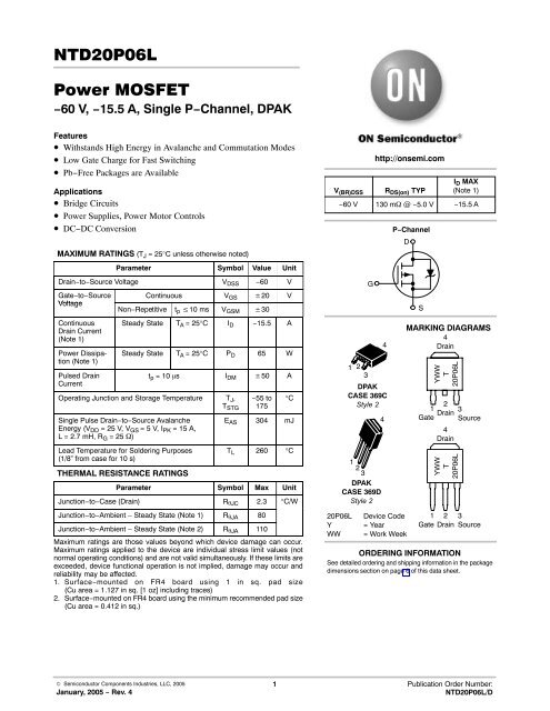
<strong>NTD20P06L</strong><br />
<strong>Power</strong> <strong>MOSFET</strong><br />
−60 V, −15.5 A, Single P−Channel, DPAK<br />
Features<br />
• Withstands High Energy in Avalanche and Commutation Modes<br />
• Low Gate Charge for Fast Switching<br />
• Pb−Free Packages are Available<br />
Applications<br />
• Bridge Circuits<br />
• <strong>Power</strong> Supplies, <strong>Power</strong> Motor Controls<br />
• DC−DC Conversion<br />
MAXIMUM RATINGS (T J = 25°C unless otherwise noted)<br />
Parameter Symbol Value Unit<br />
Drain−to−Source Voltage V DSS −60 V<br />
Gate−to−Source<br />
Voltage<br />
Continuous<br />
Drain Current<br />
(Note 1)<br />
<strong>Power</strong> Dissipation<br />
(Note 1)<br />
Pulsed Drain<br />
Current<br />
Continuous V GS 20 V<br />
Non−Repetitive t p 10 ms V GSM 30<br />
Steady State T A = 25°C I D −15.5 A<br />
Steady State T A = 25°C P D 65 W<br />
t p = 10 s I DM 50 A<br />
Operating Junction and Storage Temperature T J ,<br />
T STG<br />
Single Pulse Drain−to−Source Avalanche<br />
Energy (V DD = 25 V, V GS = 5 V, I PK = 15 A,<br />
L = 2.7 mH, R G = 25 )<br />
Lead Temperature for Soldering Purposes<br />
(1/8” from case for 10 s)<br />
THERMAL RESISTANCE RATINGS<br />
−55 to<br />
175<br />
°C<br />
E AS 304 mJ<br />
T L 260 °C<br />
Parameter Symbol Max Unit<br />
Junction−to−Case (Drain) R JC 2.3 °C/W<br />
Junction−to−Ambient – Steady State (Note 1) R JA 80<br />
Junction−to−Ambient – Steady State (Note 2) R JA 110<br />
Maximum ratings are those values beyond which device damage can occur.<br />
Maximum ratings applied to the device are individual stress limit values (not<br />
normal operating conditions) and are not valid simultaneously. If these limits are<br />
exceeded, device functional operation is not implied, damage may occur and<br />
reliability may be affected.<br />
1. Surface−mounted on FR4 board using 1 in sq. pad size<br />
(Cu area = 1.127 in sq. [1 oz] including traces)<br />
2. Surface−mounted on FR4 board using the minimum recommended pad size<br />
(Cu area = 0.412 in sq.)<br />
V (BR)DSS<br />
−60 V<br />
20P06L<br />
Y<br />
WW<br />
1 2<br />
3<br />
G<br />
DPAK<br />
CASE 369C<br />
Style 2<br />
1<br />
2<br />
3<br />
4<br />
DPAK<br />
CASE 369D<br />
Style 2<br />
http://onsemi.com<br />
4<br />
R DS(on) TYP<br />
130 m @ −5.0 V<br />
Device Code<br />
= Year<br />
= Work Week<br />
P−Channel<br />
D<br />
S<br />
MARKING DIAGRAMS<br />
4<br />
Drain<br />
1<br />
Gate<br />
1<br />
Gate<br />
YWW<br />
T<br />
20P06L<br />
2<br />
Drain<br />
4<br />
Drain<br />
YWW<br />
T<br />
20P06L<br />
2<br />
Drain<br />
I D MAX<br />
(Note 1)<br />
−15.5 A<br />
3<br />
Source<br />
3<br />
Source<br />
ORDERING INFORMATION<br />
See detailed ordering and shipping information in the package<br />
dimensions section on page 6 of this data sheet.<br />
© Semiconductor Components Industries, LLC, 2005<br />
January, 2005 − Rev. 4<br />
1 Publication Order Number:<br />
<strong>NTD20P06L</strong>/D
<strong>NTD20P06L</strong><br />
ELECTRICAL CHARACTERISTICS (T J = 25°C unless otherwise noted)<br />
Parameter Symbol Test Condition Min Typ Max Units<br />
OFF CHARACTERISTICS<br />
Drain−to−Source Breakdown Voltage V (BR)DSS V GS = 0 V, I D = −250 A −60 −74 V<br />
Drain−to−Source Breakdown Voltage<br />
Temperature Coefficient<br />
V (BR)DSS /T J −64 mV/°C<br />
Zero Gate Voltage Drain Current I DSS VGS V = 0 V,<br />
T J = 25°C −1.0 A<br />
V DS = −60 V T J = 150°C −10<br />
Gate−to−Source Leakage Current I GSS V DS = 0 V, V GS = ±20 V ±100 nA<br />
ON CHARACTERISTICS (Note 3)<br />
Gate Threshold Voltage V GS(TH) V GS = V DS , I D = −250 A −1.0 −1.5 −2.0 V<br />
Gate Threshold Temperature Coefficient V GS(TH) /T J 3.1 mV/°C<br />
Drain−to−Source On Resistance R DS(on) V GS = −5.0 V, I D = −7.5 A 0.130 0.150 <br />
( )<br />
V GS = −5.0 V, I D = −15 A 0.143<br />
Forward Transconductance g FS V DS = −10 V, I D = −7.5 A 11 S<br />
Drain−to−Source On−Voltage V DS(on) VGS V = −5.0 V,<br />
T J = 25°C −1.2 V<br />
I D = −7.5 A T J = 150°C −1.9<br />
CHARGES AND CAPACITANCES<br />
Input Capacitance C ISS 740 1190 pF<br />
Output Capacitance C OSS V GS = 0 V, f = 1 MHz, V DS = −25 V 207 300<br />
Reverse Transfer Capacitance C RSS 66 120<br />
Total Gate Charge Q G(TOT) 15 26 nC<br />
Gate−to−Source Charge Q GS<br />
V GS = −5.0 V, V DS = −48 V,<br />
I D = −18 A<br />
4.0<br />
Gate−to−Drain Charge Q GD 7.0<br />
SWITCHING CHARACTERISTICS (Note 4)<br />
Turn−On Delay Time t d(ON) 11 20 ns<br />
Rise Time t r VGS V = −5.0 V, V DD = −30 V,<br />
90 180<br />
Turn−Off Delay Time t d(OFF)<br />
I D = −15 A, R G = 9.1 28 50<br />
Fall Time t f 70 135<br />
DRAIN−SOURCE DIODE CHARACTERISTICS<br />
Forward Diode Voltage V SD T J = 25°C 1.5 2.5 V<br />
V GS = 0 V, I S = −15 A<br />
TJ = 150°C 1.3<br />
Reverse Recovery Time t RR 60 ns<br />
Charge Time t a VGS V = 0 V, d IS /d t = 100 A/s,<br />
39<br />
Discharge Time t b<br />
I S = −12 A 21<br />
Reverse Recovery Charge Q RR 0.13 nC<br />
3. Pulse Test: pulse width 300 s, duty cycle 2%<br />
4. Switching characteristics are independent of operating junction temperatures<br />
http://onsemi.com<br />
2
<strong>NTD20P06L</strong><br />
TYPICAL PERFORMANCE CURVES<br />
(T J = 25°C unless otherwise noted)<br />
−I D , DRAIN CURRENT (A)<br />
40<br />
35<br />
V GS = −10 V<br />
V GS = −9 V<br />
V GS = −6 V<br />
V GS = −5.5 V<br />
30<br />
V GS = −8 V<br />
V GS = −5 V<br />
25<br />
V GS = −7 V<br />
V GS = −4.5 V<br />
20<br />
15<br />
V GS = −4 V<br />
10<br />
V GS = −3.5 V<br />
5<br />
V GS = −3 V<br />
0<br />
T J = 25°C<br />
0 1 2 3 4 5 6 7 8 9 10<br />
−V DS , DRAIN−TO−SOURCE VOLTAGE (V)<br />
Figure 1. On−Region Characteristics<br />
−I D , DRAIN CURRENT (A)<br />
40<br />
T J = −55°C<br />
30<br />
T J = 25°C<br />
T J = 125°C<br />
20<br />
10<br />
VDS 10 V<br />
0<br />
0 1 2 3 4 5 6 7 8 9<br />
−V DS , GATE−TO−SOURCE VOLTAGE (V)<br />
Figure 2. Transfer Characteristics<br />
R DS(on) , DRAIN−TO−SOURCE RESISTANCE<br />
()<br />
0.5<br />
0.45 V GS = −5 V<br />
0.4<br />
0.35<br />
0.3<br />
0.25<br />
T J = 125°C<br />
0.2<br />
0.15<br />
T J = 25°C<br />
0.1<br />
T J = −55°C<br />
0.05<br />
0<br />
0 5 10 15 20 25 30<br />
−I D , DRAIN CURRENT (A)<br />
R DS(on) , DRAIN−TO−SOURCE RESISTANCE ()<br />
0.25<br />
0.225 T J = 25°C<br />
0.2<br />
0.175<br />
0.15<br />
V GS = −5 V<br />
0.125<br />
0.1<br />
V GS = −10 V<br />
0.075<br />
0.05<br />
0.025<br />
0<br />
0 3 6 9 12 15 18 21 24<br />
−I D , DRAIN CURRENT (A)<br />
Figure 3. On−Resistance versus Drain Current<br />
and Temperature<br />
Figure 4. On−Resistance versus Drain Current<br />
and Gate Voltage<br />
R DS(on) , DRAIN−TO−SOURCE RESISTANCE<br />
(NORMALIZED)<br />
2<br />
1.8<br />
1.6<br />
1.4<br />
1.2<br />
1<br />
0.8<br />
0.6<br />
0.4<br />
0.2<br />
I D = −7.5 A<br />
V GS = −5 V<br />
0<br />
−50 −25 0 25 50 75 100 125 150<br />
−I D , LEAKAGE (nA)<br />
10000<br />
1000<br />
100<br />
10<br />
V GS = 0 V<br />
T J = 150°C<br />
T J = 125°C<br />
1<br />
5 10 15 20 25 30 35 40 45 50 55 60<br />
T J , JUNCTION TEMPERATURE (°C)<br />
Figure 5. On−Resistance Variation with<br />
Temperature<br />
−V DS , DRAIN−TO−SOURCE VOLTAGE (V)<br />
Figure 6. Drain−to−Source Leakage Current<br />
versus Voltage<br />
http://onsemi.com<br />
3
<strong>NTD20P06L</strong><br />
C, CAPACITANCE (pF)<br />
2400<br />
2200<br />
V DS = 0 V V GS = 0 V<br />
T J = 25°C<br />
2000<br />
1800 C iss<br />
1600<br />
1400<br />
1200 C rss<br />
1000<br />
C iss<br />
800<br />
600<br />
C oss<br />
400<br />
200<br />
C rss<br />
0<br />
−10 −5 0 5 10 15 20 25<br />
−V GS −V DS<br />
GATE−TO−SOURCE OR DRAIN−TO−SOURCE<br />
VOLTAGE (V)<br />
Figure 7. Capacitance Variation<br />
−V GS , GATE−TO−SOURCE VOLTAGE<br />
(V)<br />
7.5<br />
6.25<br />
5.0<br />
3.75<br />
2.5<br />
1.25<br />
0<br />
I D = −15 A T J = 25°C<br />
V DS<br />
Q gs<br />
Q G<br />
Q GD<br />
0 4 8 12 16<br />
Q g , TOTAL GATE CHARGE (nC)<br />
V GS<br />
60<br />
50<br />
40<br />
30<br />
20<br />
10<br />
0<br />
V DS , DRAIN−TO−SOURCE VOLTAGE<br />
(V)<br />
Figure 8. Gate−to−Source and Drain−to−Source Voltage versus Total Charge<br />
t, TIME (nS)<br />
1000<br />
100<br />
10<br />
V DD = −30 V<br />
I D = −15 A<br />
V GS = −5 V<br />
t F<br />
t d(off)<br />
t R<br />
t d(on)<br />
−I S , SOURCE CURRENT (A)<br />
20<br />
15<br />
10<br />
5<br />
V GS = 0 V<br />
T J = 25°C<br />
1<br />
1 10 100<br />
R g , GATE RESISTANCE ()<br />
Figure 9. Resistive Switching Time Variation<br />
versus Gate Resistance<br />
0<br />
0 0.25 0.5 0.75 1 1.25 1.5 1.75<br />
−V SD , SOURCE−TO−DRAIN VOLTAGE (V)<br />
Figure 10. Diode Forward Voltage versus<br />
Current<br />
http://onsemi.com<br />
4
<strong>NTD20P06L</strong><br />
−I D , DRAIN CURRENT (A)<br />
1000<br />
100<br />
10<br />
1<br />
0.1<br />
V GS = −15 V<br />
Single Pulse<br />
T C = 25°C<br />
R DS(on) Limit<br />
Thermal Limit<br />
Package Limit<br />
10 ms<br />
100<br />
0.1 1 10 100<br />
−V DS , DRAIN−TO−SOURCE VOLTAGE (V)<br />
1<br />
dc<br />
EAS, SINGLE PULSE DRAIN−TO−SOURCE<br />
AVALANCHE ENERGY (mJ)<br />
350<br />
300<br />
250<br />
200<br />
150<br />
100<br />
50<br />
0<br />
I D = −15 A<br />
25 50 75 100 125 150<br />
T J , STARTING JUNCTION TEMPERATURE (°C)<br />
Figure 11. Maximum Rated Forward Biased<br />
Safe Operating Area<br />
Figure 12. Maximum Avalanche Energy versus<br />
Starting Junction Temperature<br />
R thja(t) , EFFECTIVE TRANSIENT THERMAL RESPONSE<br />
1<br />
Normalized to R JA at Steady State (1 in Pad)<br />
0.1<br />
Chip 0.0175 0.0710 0.2706 0.5776 0.7086<br />
0.0154 F 0.0854 F 0.3074 F 1.7891 F 107.55 F Ambient<br />
Single Pulse<br />
0.01<br />
1E−03 1E−02 1E−01 1E+00 1E+01 1E+02 1E+03<br />
t, TIME (s)<br />
Figure 13. Thermal Response<br />
http://onsemi.com<br />
5
<strong>NTD20P06L</strong><br />
ORDERING INFORMATION<br />
Device Package Shipping †<br />
<strong>NTD20P06L</strong>−1<br />
75 Units / Rail<br />
<strong>NTD20P06L</strong> DPAK 75 Units / Rail<br />
<strong>NTD20P06L</strong>T4<br />
<strong>NTD20P06L</strong>−1G<br />
<strong>NTD20P06L</strong>G<br />
<strong>NTD20P06L</strong>T4G<br />
DPAK<br />
(Pb−Free)<br />
2500 /Tape & Reel<br />
75 Units / Rail<br />
75 Units / Rail<br />
2500 / Tape & Reel<br />
†For information on tape and reel specifications, including part orientation and tape sizes, please refer to our Tape and Reel Packaging<br />
Specifications Brochure, BRD8011/D.<br />
http://onsemi.com<br />
6
<strong>NTD20P06L</strong><br />
PACKAGE DIMENSIONS<br />
DPAK−3<br />
CASE 369C−01<br />
ISSUE O<br />
V<br />
S<br />
F<br />
B<br />
R<br />
4<br />
1 2 3<br />
G<br />
L<br />
A<br />
K<br />
D 2 PL<br />
J<br />
H<br />
C<br />
0.13 (0.005) M T<br />
−T− SEATING<br />
PLANE<br />
E<br />
U<br />
SOLDERING FOOTPRINT*<br />
Z<br />
NOTES:<br />
1. DIMENSIONING AND TOLERANCING<br />
PER ANSI Y14.5M, 1982.<br />
2. CONTROLLING DIMENSION: INCH.<br />
INCHES MILLIMETERS<br />
DIM MIN MAX MIN MAX<br />
A 0.235 0.245 5.97 6.22<br />
B 0.250 0.265 6.35 6.73<br />
C 0.086 0.094 2.19 2.38<br />
D 0.027 0.035 0.69 0.88<br />
E 0.018 0.023 0.46 0.58<br />
F 0.037 0.045 0.94 1.14<br />
G 0.180 BSC 4.58 BSC<br />
H 0.034 0.040 0.87 1.01<br />
J 0.018 0.023 0.46 0.58<br />
K 0.102 0.114 2.60 2.89<br />
L 0.090 BSC 2.29 BSC<br />
R 0.180 0.215 4.57 5.45<br />
S 0.025 0.040 0.63 1.01<br />
U 0.020 −−− 0.51 −−−<br />
V 0.035 0.050 0.89 1.27<br />
Z 0.155 −−− 3.93 −−−<br />
STYLE 2:<br />
PIN 1. GATE<br />
2. DRAIN<br />
3. SOURCE<br />
4. DRAIN<br />
6.20<br />
0.244<br />
2.58<br />
0.101<br />
3.0<br />
0.118<br />
5.80<br />
0.228<br />
1.6<br />
0.063<br />
6.172<br />
0.243<br />
SCALE 3:1<br />
mm<br />
inches <br />
*For additional information on our Pb−Free strategy and soldering<br />
details, please download the ON Semiconductor Soldering and<br />
Mounting Techniques Reference Manual, SOLDERRM/D.<br />
http://onsemi.com<br />
7
<strong>NTD20P06L</strong><br />
PACKAGE DIMENSIONS<br />
DPAK−3<br />
CASE 369D−01<br />
ISSUE B<br />
V<br />
B<br />
R<br />
C<br />
E<br />
NOTES:<br />
1. DIMENSIONING AND TOLERANCING PER<br />
ANSI Y14.5M, 1982.<br />
2. CONTROLLING DIMENSION: INCH.<br />
S<br />
−T−<br />
SEATING<br />
PLANE<br />
F<br />
4<br />
1 2 3<br />
G<br />
A<br />
K<br />
D 3 PL<br />
J<br />
0.13 (0.005) M T<br />
H<br />
Z<br />
INCHES MILLIMETERS<br />
DIM MIN MAX MIN MAX<br />
A 0.235 0.245 5.97 6.35<br />
B 0.250 0.265 6.35 6.73<br />
C 0.086 0.094 2.19 2.38<br />
D 0.027 0.035 0.69 0.88<br />
E 0.018 0.023 0.46 0.58<br />
F 0.037 0.045 0.94 1.14<br />
G 0.090 BSC 2.29 BSC<br />
H 0.034 0.040 0.87 1.01<br />
J 0.018 0.023 0.46 0.58<br />
K 0.350 0.380 8.89 9.65<br />
R 0.180 0.215 4.45 5.45<br />
S 0.025 0.040 0.63 1.01<br />
V 0.035 0.050 0.89 1.27<br />
Z 0.155 −−− 3.93 −−−<br />
STYLE 2:<br />
PIN 1. GATE<br />
2. DRAIN<br />
3. SOURCE<br />
4. DRAIN<br />
ON Semiconductor and are registered trademarks of Semiconductor Components Industries, LLC (SCILLC). SCILLC reserves the right to make changes without further notice<br />
to any products herein. SCILLC makes no warranty, representation or guarantee regarding the suitability of its products for any particular purpose, nor does SCILLC assume any liability<br />
arising out of the application or use of any product or circuit, and specifically disclaims any and all liability, including without limitation special, consequential or incidental damages.<br />
“Typical” parameters which may be provided in SCILLC data sheets and/or specifications can and do vary in different applications and actual performance may vary over time. All<br />
operating parameters, including “Typicals” must be validated for each customer application by customer’s technical experts. SCILLC does not convey any license under its patent rights<br />
nor the rights of others. SCILLC products are not designed, intended, or authorized for use as components in systems intended for surgical implant into the body, or other applications<br />
intended to support or sustain life, or for any other application in which the failure of the SCILLC product could create a situation where personal injury or death may occur. Should<br />
Buyer purchase or use SCILLC products for any such unintended or unauthorized application, Buyer shall indemnify and hold SCILLC and its officers, employees, subsidiaries, affiliates,<br />
and distributors harmless against all claims, costs, damages, and expenses, and reasonable attorney fees arising out of, directly or indirectly, any claim of personal injury or death<br />
associated with such unintended or unauthorized use, even if such claim alleges that SCILLC was negligent regarding the design or manufacture of the part. SCILLC is an Equal<br />
Opportunity/Affirmative Action Employer. This literature is subject to all applicable copyright laws and is not for resale in any manner.<br />
PUBLICATION ORDERING INFORMATION<br />
LITERATURE FULFILLMENT:<br />
Literature Distribution Center for ON Semiconductor<br />
P.O. Box 61312, Phoenix, Arizona 85082−1312 USA<br />
Phone: 480−829−7710 or 800−344−3860 Toll Free USA/Canada<br />
Fax: 480−829−7709 or 800−344−3867 Toll Free USA/Canada<br />
Email: orderlit@onsemi.com<br />
N. American Technical Support: 800−282−9855 Toll Free<br />
USA/Canada<br />
Japan: ON Semiconductor, Japan Customer Focus Center<br />
2−9−1 Kamimeguro, Meguro−ku, Tokyo, Japan 153−0051<br />
Phone: 81−3−5773−3850<br />
http://onsemi.com<br />
8<br />
ON Semiconductor Website: http://onsemi.com<br />
Order Literature: http://www.onsemi.com/litorder<br />
For additional information, please contact your<br />
local Sales Representative.<br />
<strong>NTD20P06L</strong>/D
This datasheet has been download from:<br />
www.datasheetcatalog.com<br />
<strong>Datasheet</strong>s for electronics components.