
You also want an ePaper? Increase the reach of your titles
YUMPU automatically turns print PDFs into web optimized ePapers that Google loves.
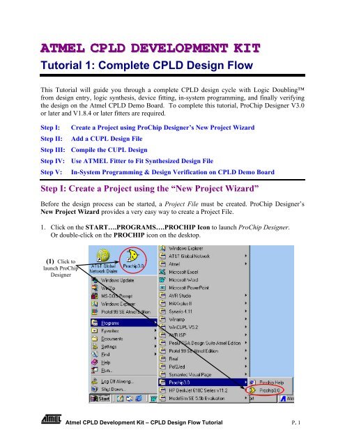
<strong>ATMEL</strong> <strong>CPLD</strong> <strong>DEVELOPMENT</strong> <strong>KIT</strong><br />
<strong>Tutorial</strong> 1: Complete <strong>CPLD</strong> Design Flow<br />
This <strong>Tutorial</strong> will guide you through a complete <strong>CPLD</strong> design cycle with Logic Doubling<br />
from design entry, logic synthesis, device fitting, in-system programming, and finally verifying<br />
the design on the Atmel <strong>CPLD</strong> Demo Board. To complete this tutorial, ProChip Designer V3.0<br />
or later and V1.8.4 or later fitters are required.<br />
Step I:<br />
Step II:<br />
Step III:<br />
Step IV:<br />
Step V:<br />
Create a Project using ProChip Designer’s New Project Wizard<br />
Add a CUPL Design File<br />
Compile the CUPL Design<br />
Use <strong>ATMEL</strong> Fitter to Fit Synthesized Design File<br />
In-System Programming & Design Verification on <strong>CPLD</strong> Demo Board<br />
Step I: Create a Project using the “New Project Wizard”<br />
Before the design process can be started, a Project File must be created. ProChip Designer’s<br />
New Project Wizard provides a very easy way to create a Project File.<br />
1. Click on the START….PROGRAMS….PROCHIP Icon to launch ProChip Designer.<br />
Or double-click on the PROCHIP icon on the desktop.<br />
(1) Click to<br />
launch ProChip<br />
Designer<br />
Atmel <strong>CPLD</strong> Development Kit – <strong>CPLD</strong> Design Flow <strong>Tutorial</strong> P. 1
2. Click on PROJECT.......NEW to launch the New Project Wizard.<br />
Or double-click on the NEW PROJECT shortcut button.<br />
3. Click on the NEW PROJECT WIZARD button to launch the New Project Wizard. This<br />
will launch the New Project Wizard to guide the users through the project creation process.<br />
(2) Click to create<br />
new project<br />
(3) Click to launch New<br />
Project Wizard<br />
4. Click on the NEXT button to start the project file creation process.<br />
(4) Click NEXT<br />
to start<br />
.<br />
Atmel <strong>CPLD</strong> Development Kit – <strong>CPLD</strong> Design Flow <strong>Tutorial</strong> P. 2
5. Use C:\PROCHIP\DESIGNS\CUPL as the directory of the project.<br />
6. Enter DEV_<strong>KIT</strong>.APJ as the project filename. The extension of a project file must be .APJ.<br />
The name and directory of the design project is specified in this window. All design, simulation,<br />
and other project files must be placed in this project directory.<br />
(5) Enter the project<br />
directory<br />
(6) Enter the project<br />
filename<br />
7. Choose a device for the project. [ATF1508AS-10JC84]. Also review the Filters that allow<br />
for selection of a specific Speed Grade or Package Type.<br />
(7) Select the<br />
device type<br />
Atmel <strong>CPLD</strong> Development Kit – <strong>CPLD</strong> Design Flow <strong>Tutorial</strong> P. 3
8. Select PROTEL SCH/CUPL as the software tool for this design flow.<br />
Protel Metamor VHDL and Protel Sch/CUPL are the two possible design flows supported by<br />
ProChip Designer. The Protel Metamor VHDL design flow supports VHDL synthesis, VHDL<br />
functional simulation and VHDL timing simulation. The Protel Sch/CUPL supports Protel<br />
Schematic and CUPL design entries and function simulation.<br />
(8) Select the<br />
design flow<br />
9. Select DONE WITH PARTS so that there will be only one device in this project.<br />
On the other hand, users can select ADD MORE PARTS to include more parts to the<br />
current Project Directory.<br />
(9) Select “Done<br />
with parts”<br />
Atmel <strong>CPLD</strong> Development Kit – <strong>CPLD</strong> Design Flow <strong>Tutorial</strong> P. 4
10. Click the FINISH button to finish the New Project Wizard and the project creation process.<br />
This closes the New Project Wizard and opens the ProChip Designer window. The Sources<br />
in the project are shown in the Left window.<br />
(10) Click FINISH<br />
to end New Project<br />
Wizard<br />
Project Sources Window<br />
Information Dialog Box<br />
Message Window<br />
Project Device Icon<br />
Atmel <strong>CPLD</strong> Development Kit – <strong>CPLD</strong> Design Flow <strong>Tutorial</strong> P. 5
11. Click on the Device Icon [ATF1508AS-10JC84] to view the Design Flow window.<br />
Design Processes<br />
Design Flow Window<br />
This completes Step I of this <strong>Tutorial</strong>.<br />
Atmel <strong>CPLD</strong> Development Kit – <strong>CPLD</strong> Design Flow <strong>Tutorial</strong> P. 6
Step II: Add a CUPL Design File<br />
Once the Project File is created, the next step is to add the design source file(s) into your project.<br />
For this tutorial, we will be adding a single CUPL design file into the project.<br />
1. Click on the ADD/EDIT button from Source Manager to open the Source Manager Window.<br />
You can view the Source Manager Help File by clicking on the Help button within the<br />
Source Manager Window to view the description for the different processes.<br />
2. In the Source Manager Window, click on the ADD button to add a CUPL design file to the<br />
project.<br />
3. In the File Manager Window, select LOGIC_D.PLD from the c:\Prochip\designs\cupl<br />
directory as the source design file for this project.<br />
(1) Click<br />
Add/Edit to open<br />
Source Manger<br />
Window<br />
(2) Click Add<br />
to add design<br />
file<br />
(3) Select<br />
CUPL source<br />
file<br />
This “LOGIC_D.PLD” is a CUPL design that uses the eight 8-segment LED displays and the<br />
built-in oscillator on the Atmel <strong>CPLD</strong> Demo Board to first display the word “logic” and then<br />
switches to the word “doubling”. This CUPL design can be compiled using either the ProChip<br />
Designer or the Atmel-WinCUPL ® software.<br />
The first section of the LOGIC_D.PLD as shown below pre-defines which segments of the LED<br />
should be asserted in order to display the desired letter or number. For example, to display the<br />
letter “C”, segments A, D, E, and F need to be set to low and the remaining segments need to be<br />
set to high.<br />
Atmel <strong>CPLD</strong> Development Kit – <strong>CPLD</strong> Design Flow <strong>Tutorial</strong> P. 7
$define Font0 'b'1000000 /* = ( _f_e_d_c_b_a ); 0 */<br />
$define Font1 'b'1111001 /* = ( _c_b ); 1 */<br />
$define Font2 'b'0100100 /* = (_g _e_d _b_a ); 2 */<br />
$define Font3 'b'0110000 /* = (_g _d_c_b_a ); 3 */<br />
$define Font4 'b'0011001 /* = (_g_f _c_b ); 4 */<br />
$define Font5 'b'0010010 /* = (_g_f _d_c _a ); 5 */<br />
$define Font6 'b'0000010 /* = (_g_f_e_d_c _a ); 6 */<br />
$define Font7 'b'1111000 /* = ( _c_b_a ); 7 */<br />
$define Font8 'b'0000000 /* = (_g_f_e_d_c_b_a ); 8 */<br />
$define Font9 'b'0011000 /* = (_g_f _c_b_a ); 9 */<br />
$define FontA 'b'0001000 /* = (_g_f_e _c_b_a ); A */<br />
$define FontC 'b'1000110 /* = ( _f_e_d _a ); C */<br />
The next section of this PLD design as shown below shows you how to declare and assign pin<br />
numbers in the CUPL language to the input, output, and buried signals. The input and output pin<br />
assignments are assigned according to the connections between the <strong>CPLD</strong> and the eight 8-<br />
segment LED’s as shown in the <strong>CPLD</strong> Demo Board schematic.<br />
/* Inputs */<br />
pin 1 = Gclr; /* Global Clear input */<br />
pin 83 = Mclk; /* Global Clock input */<br />
/* Outputs */<br />
/* DSP1 */<br />
pin 49 = LED1A; /* LED1 segment A */<br />
pin 46 = LED1B; /* LED1 segment B */<br />
pin 48 = LED1C; /* LED1 segment C */<br />
pin 50 = LED1D; /* LED1 segment D */<br />
pin 52 = LED1E; /* LED1 segment E */<br />
pin 51 = LED1F; /* LED1 segment F */<br />
pin 54 = LED1G; /* LED1 segment G */<br />
Next the pinnode numbers are assigned to the buried signals as shown below. The feedback<br />
and/or the foldback paths available in each macrocell implement these buried signals. For the<br />
listing of the pinnode numbers, please refer to the “ATF15xx Device Help” section of the<br />
ProChip Designer Help File.<br />
/* Nodes for the buried 22-bit Counter */<br />
pinnode 603 = c0;<br />
pinnode 605 = c1;<br />
pinnode 606 = c2;<br />
pinnode 608 = c3;<br />
After assigning the input, output and buried signals, the related signals (e.g. the LED segments<br />
and buried counter) are grouped together as shown below to make the design source code more<br />
readable and easier to manage. In CUPL, the “Field” declaration can be used to group a specific<br />
set of signals.<br />
Atmel <strong>CPLD</strong> Development Kit – <strong>CPLD</strong> Design Flow <strong>Tutorial</strong> P. 8
Field DSP1 = [LED1G,LED1F,LED1E,LED1D,LED1C,LED1B,LED1A];<br />
Field DSP2 = [LED2G,LED2F,LED2E,LED2D,LED2C,LED2B,LED2A];<br />
Field DSP3 = [LED3G,LED3F,LED3E,LED3D,LED3C,LED3B,LED3A];<br />
Field DSP4 = [LED4G,LED4F,LED4E,LED4D,LED4C,LED4B,LED4A];<br />
Field DSP5 = [LED5G,LED5F,LED5E,LED5D,LED5C,LED5B,LED5A];<br />
Field DSP6 = [LED6G,LED6F,LED6E,LED6D,LED6C,LED6B,LED6A];<br />
Field DSP7 = [LED7G,LED7F,LED7E,LED7D,LED7C,LED7B,LED7A];<br />
Field DSP8 = [LED8G,LED8F,LED8E,LED8D,LED8C,LED8B,LED8A];<br />
Field Count = [c21..c0] ;<br />
Next a 22-bit buried counter using T-type Flip-flops is implemented as shown below to divide<br />
the 2.0MHz clock into a much slower frequency signal that can be used to display the text<br />
messages. The last bit of this counter (c21) will be a periodic square wave signal oscillating at<br />
0.477Hz (2MHz ÷ 2 22 = 2×10 6 ÷ 4194304 = 0.477Hz).<br />
/* Frequency Divider */<br />
c0.d = !c0;<br />
c1.t = c0;<br />
c2.t = c1 & c0;<br />
c3.t = c2 & c1 & c0;<br />
:<br />
:<br />
c20.t = c19 & c18 & c17 & c16 & c15 & c14 & c13 & c12 & c11 & c10 & c9<br />
& c8 & c7 & c6 & c5 & c4 & c3 & c2 & c1 & c0;<br />
c21.t = c20 & c19 & c18 & c17 & c16 & c15 & c14 & c13 & c12 & c11 &<br />
c10 & c9 & c8 & c7 & c6 & c5 & c4 & c3 & c2 & c1 & c0;<br />
Count.ck = Mclk;<br />
Count.ar = !Gclr;<br />
Finally, the last section of the PLD design is to assign the eight 8-segment LED displays to the<br />
appropriate letters or numbers as shown below to display the words “logic” and “doubling”. The<br />
word “logic” is displayed when c21 is low and then “doubling” is displayed when c21 is high.<br />
You can easily change the letters/numbers to be displayed by changing this section of the code to<br />
the appropriate pre-defined letters/numbers.<br />
DSP8 = Fontl & !c21 # Fontd & c21;<br />
DSP7 = Fonto & !c21 # Fonto & c21;<br />
DSP6 = Fontg & !c21 # Fontu & c21;<br />
DSP5 = Fonti & !c21 # Fontb & c21;<br />
DSP4 = Fontc & !c21 # Fontl & c21;<br />
DSP3 = FontBK & !c21 # Fonti & c21;<br />
DSP2 = FontBK & !c21 # Fontn & c21;<br />
DSP1 = FontBK & !c21 # Fontg & c21;<br />
You have now completed Step II of this <strong>Tutorial</strong>.<br />
Atmel <strong>CPLD</strong> Development Kit – <strong>CPLD</strong> Design Flow <strong>Tutorial</strong> P. 9
Step III: Compile the CUPL Design<br />
In this step, you will compile your CUPL design through Protel Design Explorer 99 SE into a set<br />
of optimized/minimized logic equations.<br />
1. Click on the COMPILE LOGIC button in the Design Flow Window to open the Logic<br />
Synthesis Window.<br />
(1) Open Logic<br />
Synthesis<br />
Window<br />
2. Make sure all of the options in the Optimization section are unchecked.<br />
3. Make sure the Minimization setting is set to QUICK.<br />
4. Click on the COMPILE button to start the CUPL compile process.<br />
(2) Make sure<br />
these options are<br />
unchecked<br />
(3) Set<br />
Minimization to<br />
Quick<br />
(4) Start the<br />
Compile process<br />
Atmel <strong>CPLD</strong> Development Kit – <strong>CPLD</strong> Design Flow <strong>Tutorial</strong> P. 10
You can click on the SET DEFAULTS button and it will automatically specify the Synthesis<br />
tool in the Tool Text box.<br />
If you click on the CUPL Tab, it shows the various Synthesis options. You may refer to the<br />
HELP file for further description.<br />
This completes Step III of this <strong>Tutorial</strong>.<br />
Atmel <strong>CPLD</strong> Development Kit – <strong>CPLD</strong> Design Flow <strong>Tutorial</strong> P. 11
Step IV: Use <strong>ATMEL</strong> Fitter to Fit the Synthesized Design File<br />
In Step III, we completed the Logic Synthesis portion of the Design Flow. On successful<br />
compilation, the CUPL compiler tool produces a PLA output file (with extension .pla). A PLA<br />
file contains the netlist of the optimized and minimized logic equations. We now need to map<br />
this netlist into a specific Atmel PLD architecture using the <strong>ATMEL</strong> FITTER.<br />
1. You can now proceed to the Device Fitter portion of the Design Flow by clicking on the<br />
<strong>ATMEL</strong> FITTER button.<br />
(1) Open the<br />
Atmel Fitter<br />
Window<br />
You can either use the Default options or specify Fitter properties. You must select a PLA file or<br />
the Fitter will not run. In this example, since our target device is an ATF1508AS, and we will<br />
select the fit1508.exe device fitter.<br />
The fitter creates the important JEDEC and FIT REPORT output files. They contain the data for<br />
programming the Device (using In-System Programming or on a third party device programmer)<br />
and the pin assignments required for board layout respectively.<br />
Atmel <strong>CPLD</strong> Development Kit – <strong>CPLD</strong> Design Flow <strong>Tutorial</strong> P. 12
Please review the Global Device Parameters and Pin/Node Options as well. The Help Files also<br />
show the Device Pin_Node lists for each of the <strong>ATMEL</strong> <strong>CPLD</strong>s.<br />
2. Make sure the JTAG box is checked. This enables the JTAG port for ISP programming.<br />
3. Make sure the PIN FIT CONTROL setting is set to KEEP. This will ensure that the pin<br />
assignments in the PLD file will be kept during the Place-and-Route process.<br />
4. Make sure all of the options in the LOGIC NODE DEFAULTS section are unchecked.<br />
5. Change the Logic Double control to always. This enables the fitter to use ATF15xx Family<br />
devices Logic Doubling features beginning in the first fitter pass.<br />
6. When all the fitter options are set, click on the RUN FITTER button to fit the design.<br />
(2) Check the<br />
JTAG box<br />
(4) Make sure all<br />
options are<br />
unchecked<br />
(3) Change the<br />
Pin Fit Control<br />
setting to Keep<br />
(6) Start the<br />
fitting process<br />
(5) Set Logic Double<br />
to “always”<br />
Atmel <strong>CPLD</strong> Development Kit – <strong>CPLD</strong> Design Flow <strong>Tutorial</strong> P. 13
The Fitter Report File is shown below.<br />
Atmel ATF1508AS Fitter Version 1.8.3.9 ,running Thu Jul 05 19:30:31 2001<br />
fit1508 -i C:\FITTER\TEST\V1839\LOGIC_D\LOGIC_D.tt2 -CUPL -dev P1508C84 -JTAG ON<br />
****** Initial fitting strategy and property ******<br />
Pla_in_file = LOGIC_D.tt2<br />
Pla_out_file = LOGIC_D.tt3<br />
Jedec_file = LOGIC_D.jed<br />
Vector_file = LOGIC_D.tmv<br />
verilog_file = LOGIC_D.vt<br />
:<br />
:<br />
:<br />
** Resource Usage **<br />
pin_num pin_name output_type feedback foldback cascade_out TotPT output_slew<br />
MC1 0 -- -- -- -- -- 0 slow<br />
MC2 0 -- -- -- -- -- 0 slow<br />
MC3 12 LED6B reg c0 -- -- 2 slow<br />
MC4 0 -- -- -- -- -- 0 slow<br />
MC5 11 LED5G reg c1 -- -- 3 slow<br />
MC6 10 LED5E reg c2 -- -- 3 slow<br />
MC7 0 -- -- -- -- -- 0 slow<br />
MC8 9 LED5F reg c3 -- -- 3 slow<br />
MC9 0 -- -- -- -- -- 0 slow<br />
MC10 0 -- -- -- -- -- 0 slow<br />
:<br />
:<br />
ATF15xx Family devices Logic Doubling features provide extra IO connectivity and logic<br />
reusability. For example, every pin has the option of individual output enable, and every<br />
macrocell has the option of feedback of either the registered or combinatorial output<br />
independently of which signal is routed to the pin driver.<br />
In the LOGIC_D example given here, Macrocells 3, 5, 6 etc. route their combinatorial outputs,<br />
LED6B, LED5G, LED5E, etc. to the pins while also routing their registered outputs, c0, c1, c2<br />
etc. to the feedback outputs, thus doubling the utilization of the macrocell logic.<br />
For more examples of design techniques that utilize the Logic Doubling features of the ATF15xx<br />
Family, refer to Atmel’s Logic Doubling White Paper and Reference Designs, available on the<br />
Atmel website at http://www.atmel.com/atmel/products/prod147.htm#refdsgns.zip These<br />
examples show how to apply Logic Doubling techniques to new product designs, and obtain the<br />
benefits of more features in a smaller, and possibly less expensive chip, or spare logic resources<br />
for future revisions and reduced risk of PCB re-spin.<br />
This completes Step IV of this <strong>Tutorial</strong>.<br />
Atmel <strong>CPLD</strong> Development Kit – <strong>CPLD</strong> Design Flow <strong>Tutorial</strong> P. 14
Step V: In-System Programming and Design Verification<br />
In this step of the tutorial, you will program an ATF1508AS 84-pin PLCC device on the Atmel<br />
<strong>CPLD</strong> Demo Board through ISP and then verify the design by observing the text messages<br />
displayed on the eight 8-segment LED displays on the Development Kit.<br />
You will need to initialize the ATMISP software in order to program the ATF1508AS 84-pin<br />
PLCC on the <strong>CPLD</strong> Demo Board.<br />
1. Click on the START….PROGRAMS….ATMISP Icon to launch the Atmel-ISP Software<br />
Or double-click on the ATMISP icon on the desktop.<br />
(1) Click to launch<br />
ATMISP<br />
2. Enter “1” as the number of devices in your JTAG device chain and then click on the OK<br />
button to proceed to the next step.<br />
(2) Enter “1” as the<br />
number of devices<br />
Atmel <strong>CPLD</strong> Development Kit – <strong>CPLD</strong> Design Flow <strong>Tutorial</strong> P. 15
3. Select ATF1508AS as the target device type.<br />
4. Select PROGRAM/VERIFY as the JTAG Instruction type.<br />
5. Select “C:\PROCHIP\DESIGNS\CUPL\LOGIC_D.JED” as the JEDEC file to be<br />
programmed into the ATF1508AS and then click on the OK button to proceed to the next<br />
step.<br />
(3) Select<br />
ATF1508AS<br />
(4) Select<br />
Program/Verify<br />
(5) Select the<br />
JEDEC file<br />
The next step requires you to setup the Atmel <strong>CPLD</strong> Demo Board to program the<br />
ATF1508AS through ISP.<br />
6. Connect the 25-DB side of the Atmel-ISP Cable to the PC’s parallel port and the 10-pin<br />
header side to the Atmel-ISP Cable to the Atmel <strong>CPLD</strong> Demo Board as shown below.<br />
Atmel <strong>CPLD</strong> Development Kit – <strong>CPLD</strong> Design Flow <strong>Tutorial</strong> P. 16
7. Connect a 9V AC/DC power adapter to the power connector (JPower) of the Atmel<br />
<strong>CPLD</strong> Demo Board.<br />
8. Set the 5V/3.3V jumper to 5V to set the system Vcc to 5V.<br />
9. Set the JPCLK jumper to PIN83 so that the output of the crystal oscillator will go to Pin<br />
83 of the ATF1508AS.<br />
10. Switch the Power Switch to the ON position.<br />
(9) Set JPCLK to<br />
PIN83<br />
(7) Power<br />
Connector<br />
(10) Set the<br />
Power Switch to ON<br />
(8) Set Vcc to 5V<br />
Now both your software and hardware are setup for ISP programming, and you can execute<br />
the PROGRAM/VERIFY instruction to program the ATF1508AS on the Atmel <strong>CPLD</strong> Demo<br />
Board.<br />
11. Click on the LAUNCH button in the ATMISP main window to execute the JTAG<br />
instruction to program the ATF1508AS on the Development Kit.<br />
(11) Click on<br />
the Launch button<br />
Atmel <strong>CPLD</strong> Development Kit – <strong>CPLD</strong> Design Flow <strong>Tutorial</strong> P. 17
After the successfully programming the ATF1508AS with the LOGIC_D.JED file, the eight<br />
8-segment LED’s should first display the word “logic” and then the word “doubling”.<br />
If these two text messages are correctly displayed on the Development Kit, then you have<br />
successfully completed this tutorial.<br />
Congratulations!<br />
Atmel <strong>CPLD</strong> Development Kit – <strong>CPLD</strong> Design Flow <strong>Tutorial</strong> P. 18