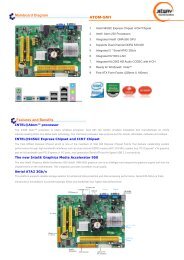
User's Manual - Jetway Computer
User's Manual - Jetway Computer
User's Manual - Jetway Computer

Create successful ePaper yourself
Turn your PDF publications into a flip-book with our unique Google optimized e-Paper software.
TECHNICAL MANUAL<br />
Of<br />
VIA VX800<br />
Based<br />
Mini-ITX M/B For VIA C7/Eden/Nano<br />
Processor<br />
NO.G03-NF77-F<br />
Rev.2.0<br />
Release date: December, 2008<br />
Trademark:<br />
* Specifications and Information contained in this documentation are furnished for information use only, and are<br />
subject to change at any time without notice, and should not be construed as a commitment by manufacturer.
Environmental Protection Announcement<br />
Do not dispose this electronic device into the trash while discarding. To minimize pollution<br />
and ensure environment protection of mother earth, please recycle.<br />
ii
TABLE OF CONTENT<br />
USER’S NOTICE .................................................................................................................................. iv<br />
MANUAL REVISION INFORMATION ............................................................................................ iv<br />
ITEM CHECKLIST.............................................................................................................................. iv<br />
CHAPTER 1 INTRODUCTION OF MOTHERBOARD<br />
1-1 FEATURE OF MOTHERBOARD..............................................................................……1<br />
1-2 SPECIFICATION.................................................................................................................. 2<br />
1-3 LAYOUT DIAGRAM & JUMPER SETTING................................................................... 3<br />
CHAPTER 2 HARDWARE INSTALLATION<br />
2-1 JUMPER SETTING ..............................................................................................................7<br />
2-2 CONNECTORS AND HEADERS ....................................................................................... 10<br />
2-2-1 CONNECTORS....................................................................................................... 10<br />
2-2-2 HEADERS ............................................................................................................... 10<br />
CHAPTER 3 INTRODUCING BIOS<br />
3-1 ENTERING SETUP .............................................................................................................. 16<br />
3-2 GETTING HELP................................................................................................................... 16<br />
3-3 THE MAIN MENU................................................................................................................ 16<br />
3-4 STANDARD BIOS FEATURES........................................................................................... 18<br />
3-5 ADVANCED BIOS FEATURES.......................................................................................... 20<br />
3-5-1 CPU FEATURE....................................................................................................... 23<br />
3-6 ADVANCED CHIPSET FEATURES.................................................................................. 23<br />
3-6-1 DRAM TIMING SETTINGS ................................................................................. 24<br />
3-6-2 VGA TIMING SETTINGS..................................................................................... 25<br />
3-6-3 PCI TIMING SETTINGS....................................................................................... 25<br />
3-7 INTEGRATED PERIPHERALS ......................................................................................... 26<br />
3-7-1 ONBOARD IDE FUNCTION................................................................................. 26<br />
3-7-2 ONBOARD DEVICE FUNCTIONS...................................................................... 27<br />
3-7-3 ONBOARD SUPERIO FUNCTIONS.................................................................... 28<br />
3-7-4 USB DEVICE SETTINGS...................................................................................... 30<br />
3-8 POWER MANAGERMENT SETUP................................................................................... 31<br />
3-9 PNP/PCI CONFIGURATION.............................................................................................. 32<br />
3-10 PC HEALTH STATUS.......................................................................................................... 33<br />
3-11 MISCELLANEOUS CONTROL ......................................................................................... 34<br />
iii
3-12 PASSWORD SETTING ........................................................................................................ 35<br />
3-13 LOAD STANDARD/OPTIMIZED DEFAULTS ................................................................ 36<br />
USER’S NOTICE<br />
COPYRIGHT OF THIS MANUAL BELONGS TO THE MANUFACTURER. NO PART OF THIS MANUAL,<br />
INCLUDING THE PRODUCTS AND SOFTWARE DESCRIBED IN IT MAY BE REPRODUCED,<br />
TRANSMITTED OR TRANSLATED INTO ANY LANGUAGE IN ANY FORM OR BY ANY MEANS WITHOUT<br />
WRITTEN PERMISSION OF THE MANUFACTURER.<br />
THIS MANUAL CONTAINS ALL INFORMATION REQUIRED TO USE VIA VX800 CHIPSET<br />
MOTHER-BOARD SERIES AND WE DO ASSURE THIS MANUAL MEETS USER’S REQUIREMENT BUT WILL<br />
CHANGE, CORRECT ANY TIME WITHOUT NOTICE. MANUFACTURER PROVIDES THIS MANUAL “AS IS”<br />
WITHOUT WARRANTY OF ANY KIND, AND WILL NOT BE LIABLE FOR ANY INDIRECT, SPECIAL,<br />
INCIDENTIAL OR CONSEQUENTIAL DAMAGES (INCLUDING DAMANGES FOR LOSS OF PROFIT, LOSS OF<br />
BUSINESS, LOSS OF USE OF DATA, INTERRUPTION OF BUSINESS AND THE LIKE).<br />
PRODUCTS AND CORPORATE NAMES APPEARING IN THIS MANUAL MAY OR MAY NOT BE<br />
REGISTERED TRADEMARKS OR COPYRIGHTS OF THEIR RESPECTIVE COMPANIES, AND THEY ARE<br />
USED ONLY FOR IDENTIFICATION OR EXPLANATION AND TO THE OWNER’S BENEFIT, WITHOUT<br />
INTENT TO INFRINGE.<br />
<strong>Manual</strong> Revision Information<br />
Reversion Revision History Date<br />
2.0 Second Edition December, 2008<br />
Item Checklist<br />
Motherboard<br />
Cable(s)<br />
CD for motherboard utilities<br />
Motherboard User’s <strong>Manual</strong><br />
I/O Back panel Shield<br />
iv
Introduction of the Motherboard<br />
Chapter 1<br />
1-1 Feature of motherboard<br />
* VIA VX800 chipset.<br />
*Onboard optional C7/Eden/Nano CPU, with low power consumption and never denies high<br />
performance.<br />
* Support optional FSB 400/533 /800MHz.<br />
* Support DDRII 400/533/667 up to 2GB.<br />
* Onboard REALTEK RTL 8111C Gigabit Ethernet LAN.<br />
* Integrated VIA 1708 B 6-channel HD audio CODEC<br />
* Support USB2.0 data transport demands.<br />
1
1-2 Specification<br />
Spec<br />
Design<br />
Chipset<br />
Embedded CPU<br />
Memory Socket<br />
x Expansion Slots<br />
Integrate IDE<br />
LAN<br />
Audio<br />
BIOS<br />
Multi I/O<br />
Description<br />
∗ Mini ITX form factor 4 layers PCB size: 17.0x17.0cm<br />
∗ VIA VX800 Chipset<br />
∗ Optional VIA C7 /Eden/Nano seriesCPU<br />
∗ 240-pin DDRII DIMM socket x1<br />
∗ Support DDRII 400/533/667MHz system Modules DDR memory<br />
∗ Expandable to 2GB.<br />
∗ 32-bit PCI slot x 1pcs<br />
∗ One PCI IDE controller that supports PCI Bus Mastering, ATA<br />
PIO/DMA and the ULTRA DMA 133/100/66 functions that<br />
deliver the data transfer rate up to 133 MB/s;<br />
∗ Integrated Realtek RTL8111C PCI-E LAN chip.<br />
∗ Support Fast Ethernet LAN function of providing<br />
10Mb/100Mb/1000Mb Ethernet data transfer rate<br />
∗ VIA 1708B 6-channel Audio Codec integrated<br />
∗ Audio driver and utility included<br />
∗ Award 4MB Flash ROM<br />
∗ PS/2 keyboard and PS/2 mouse connectors<br />
∗ Serial port connector x1/Parallel connector x1<br />
∗ VGA connectorx1<br />
∗ USB2.0 port x 4<br />
∗ RJ45 LAN connector x1<br />
∗ Audio connector x1 (Line-in, Line-out, MIC/ 6CH Audio)<br />
∗ LVDS inverter connector x1<br />
∗ LCD header x1<br />
∗ COM header x 3<br />
2
∗ IR header x1<br />
∗ Wi-Fi header x1<br />
∗ Audio header x 1/ CDIN header x1<br />
∗ Front Panel header x1<br />
∗ Hard disk drive connector x1<br />
∗ SATAII connector x2<br />
1-3 Layout Diagram<br />
PS/2<br />
Mouse<br />
PS/2<br />
Keyboard<br />
Parallel Port<br />
Connector<br />
RJ45 LAN<br />
Line-In<br />
Line-Out<br />
MIC-IN<br />
Serial Port<br />
Connector<br />
VGA<br />
Connector<br />
USB<br />
Connector<br />
USB<br />
Connector<br />
3
Keyboard/ USB Power (JP2)<br />
ATX Power Connector<br />
PS2 KB/Mouse Port<br />
JP8<br />
Parallel Port Connector<br />
over<br />
Serial Port Connector &<br />
VGA connector<br />
Serial Port<br />
Header<br />
CPU FAN<br />
VIA C7/Eden/Nano<br />
Series CPU<br />
SYS FAN1<br />
DDRII Socket x1<br />
USB Port Connector<br />
RealtekRTL8111C<br />
Gigabit Lan<br />
RJ-45 over USB<br />
Connector<br />
IR Connector<br />
LVDS<br />
Inverter<br />
JP4<br />
JP5<br />
VIA VX800<br />
LVDS Header<br />
SATAII Connectors<br />
IDE Connector<br />
Audio Connector<br />
CD Audio-In<br />
Header<br />
VIA 1708B<br />
JP3<br />
Serial Port<br />
Headers<br />
Speaker connector<br />
Power LED<br />
JBAT<br />
Front Panel Audio<br />
Wi-Fi Header<br />
PCI Slot<br />
SYS FAN2<br />
Front Panel Header<br />
4
Jumper<br />
Jumper Name Description Page<br />
JP2 KB/USB Power On Function Setting 3-pin Block P.7<br />
JBAT CMOS RAM Clear Function Setting 3-pin Block P.7<br />
JP3 USB Power On Function Setting 3-pin Block P.8<br />
JP4 LVDS Voltage 5V/3.3V Select 3-pin Block P.8<br />
JP5 LVDS Inverter Power On Setting 3-pin Block P.9<br />
JP8 Power RS232 Function Select 6-pin Block P.9<br />
Connectors<br />
Connector Name Description Page<br />
PS2KBMS1 Keyboard & Mouse Connector 6-pin Female Connector p.10<br />
COM1 Serial Port Connector 9-pin Connector p.10<br />
VGA Video Graphic Attach Connector D-sub 15-pin Female p.10<br />
PARALLEL Parallel Port Connector 25-Pin Connector p.10<br />
USB1,USB2 USB Port Connector 4-pin Connector p.10<br />
RJ-45 from UL2 RJ-45 LAN Connector 8-pin Connector p.10<br />
AUDIO1 Line-Out /MIC/Line-In Audio Connector 3 Phone Jack p.10<br />
IDE1 IDE Hard Disk Drive Connector 40-pin IDE Block<br />
SATA1,2 Serial ATA Connectors 7-pin Connector<br />
5
Headers<br />
Header Name Description Page<br />
AUDIO Front panel audio Headers 9-pin block P.11<br />
CDIN CD Audio-In Header 4-pin Block P.12<br />
COM 2,3,4 Serial Port COM1 Connector 9-pin Block p.12<br />
WI-FI Wi-Fi Header 11-pin Block P.13<br />
LCD LVDS Connector 32-pin Block P.13<br />
Inverter LVDS Inverter Connector 7-pin Block P.14<br />
IR IR infrared module Headers 5-pin Block P.15<br />
SPEAK Speaker Header 3-pin Block P.15<br />
PWR LED Power LED 4-pin Block P.16<br />
JW_FP<br />
(PWR LED/ IDE LED/<br />
/Power Button /Reset)<br />
SFAN1,<br />
FAN<br />
Front Panel Header<br />
(PWR LED/ IDE LED/ /Power Button<br />
/Reset)<br />
9-pin Block P.16<br />
SFAN2,CPU FAN Headers 3-pin Block P.16<br />
6
2-1 Jumper Setting<br />
Chapter 2<br />
(1) JP2: KB/USB Power On Function Setting<br />
JP2<br />
1 3<br />
JP2<br />
1 3<br />
1-2 K.B&USBPOWER-ON Disacled(default)<br />
2-3 K.B& USB POWER-ON Enabled<br />
(2) JBAT : Clear CMOS (3-pin)<br />
JBAT<br />
1<br />
JBAT<br />
1<br />
3<br />
3<br />
1-2 closed Normal<br />
2-3 closed Clear CMOS<br />
CMOS RAM Clear Setting<br />
7
(3) JP3: USB Power On Function Setting (3-pin)<br />
JP3<br />
1 3<br />
JP3<br />
1 3<br />
1-2 USB Power-on Disacled(default)<br />
2-3 USB Power-on Enabled<br />
(4) JP4: LVDS VDD setting (3-pin)<br />
JP4<br />
1 3 1 3<br />
JP4<br />
1-2 closed: 5V<br />
2-3 closed : 3.3V<br />
LVDS VDD setting<br />
8
(5) JP5: LVDS Inverter Backlight Setting (3-pin)<br />
JP5<br />
1<br />
3<br />
JP5 1<br />
3<br />
1-2 closed: Off<br />
2-3 closed : On<br />
LVDS Inverter Backlight Setting<br />
(6) JP8: Powered RS232 Function Select<br />
JP8<br />
1<br />
1<br />
1<br />
1-2 closed: RS232<br />
3-4 closed : +12V<br />
5-6 closed : +5V<br />
9
2-2 Connectors and Headers<br />
2-2-1 Connectors<br />
(1) I/O Back Panel Connector<br />
RJ45 LAN<br />
PS/2<br />
Keyboard<br />
PS/2<br />
Mouse<br />
Parallel Port<br />
Connector<br />
Line-In<br />
Line-Out<br />
MIC-IN<br />
2-2-2 Headers<br />
(1) Front panel audio header (9-pin): AUDIO<br />
Serial Port<br />
Connector<br />
USB<br />
VGA<br />
Connector<br />
Connector<br />
USB<br />
Connector<br />
AUDIO<br />
Pin 1<br />
Lineout2-R<br />
Sense-FB<br />
Lineout2-L<br />
Audio-GND<br />
Audio-JD<br />
LINE2-JD<br />
2<br />
10<br />
9<br />
MIC2-L<br />
MIC2-R<br />
MIC2-JD<br />
KEY<br />
10<br />
Line-Out, MIC Headers
(2) CD AUDIO-In Headers (4-pin): CDIN<br />
1<br />
4<br />
CD-L<br />
GND<br />
GND<br />
CD-R<br />
CD Audio-In Headers<br />
(3) COM Connectors (9-pin): COM2/COM3/COM4<br />
Pin1<br />
DCD<br />
RXD<br />
TXD<br />
DTR<br />
GND<br />
DSR<br />
RTS<br />
GTS<br />
RI<br />
Serial Port 9-pin Block<br />
(4)Wi-Fi header: WI-FI<br />
This header supports WI-FI Function. Connect the wireless local area network adapter to this<br />
header. It allows you to create a wireless environment and enjoy the convenience of wireless<br />
network connectivity.<br />
11
WI-FI<br />
2<br />
Pin 1<br />
USB+5<br />
D0-<br />
D0+<br />
GND<br />
USB+5<br />
D1-<br />
D1+<br />
GND<br />
N.C<br />
+3.3V<br />
12<br />
11<br />
N.C<br />
WI-FI Headers<br />
(5)LVDS Headers: LCD Pin NO. Pin<br />
Define<br />
Pin<br />
NO.<br />
Pin Define<br />
Pin 1 R2IN3- Pin 2 R2IN3+<br />
Pin 3 CK2IN- Pin 4 CK2IN+<br />
Pin 5 R2IN2- Pin 6 R2IN2+<br />
Pin 7 R2IN1- Pin 8 R2IN1+<br />
Pin 9 R2IN0- Pin 10 R2IN0+<br />
Pin 11 GND Pin 12 GND<br />
Pin 13 GND Pin 14 GND<br />
Pin 15 GND Pin 16 GND<br />
Pin 17 R1IN3+ Pin 18 R1IN3-<br />
CN1<br />
Pin 19 CK1IN+ Pin 20 CK1IN-<br />
Pin 21 R1IN2+ Pin 22 R1IN2-<br />
LVDS Headers<br />
Pin 23 R1IN1+ Pin 24 R1IN1-<br />
Pin 25 R1IN0+ Pin 26 R1IN0-<br />
Pin 27 VDD Pin 28 VDD<br />
Pin 29 VDD Pin 30 VDD<br />
Pin 31 GND Pin 32 GND<br />
12
(6)Pin-headers of LVDS Inverter: INVERTER<br />
PIN No.<br />
Symbol<br />
Pin 1<br />
1 +12VIN<br />
LVDS Inverter<br />
2 +12VIN<br />
3 GND<br />
4 GND<br />
5 LVDS Panel backlight<br />
enable<br />
6 GND<br />
7 Panel backlight<br />
(7) IR infrared module Headers (5-pin): IR<br />
brightness control<br />
IR<br />
GND<br />
IRRX<br />
2<br />
6<br />
Pin 1<br />
5<br />
NC<br />
+5V<br />
IRTX<br />
IR infrared module Header<br />
13
(8) Speaker Header & Power Led Header(9-pin): SPEAK/ PWRLED<br />
Pin 1<br />
Pin 1<br />
PWRLED<br />
SPEAK<br />
SPKR<br />
NC<br />
GND<br />
VCC5<br />
SPEAK & PWRLED Header<br />
(9) Front Panel Header(9-pin): JW_FP<br />
JW FP<br />
HDLED<br />
RESET<br />
VCC5<br />
HDDLE<br />
GND<br />
RSTSW<br />
NC<br />
VCC5 PWR LED<br />
PWRLED<br />
PWRBTN<br />
GND PWRBTN<br />
Pin 1<br />
Front Panel Headers<br />
14
(10) FAN Speed Headers (3-pin): CPUFAN, SFAN1/SFAN2<br />
+12v<br />
Fan<br />
GND power<br />
Fan<br />
clock<br />
3<br />
1<br />
Fan Headers<br />
Introducing BIOS<br />
Chapter 3<br />
The BIOS is a program located on a Flash Memory on the motherboard. This program is a<br />
bridge between motherboard and operating system. When you start the computer, the BIOS<br />
program will gain control. The BIOS first operates an auto-diagnostic test called POST (power<br />
on self test) for all the necessary hardware, it detects the entire hardware device and<br />
configures the parameters of the hardware synchronization. Only when these tasks are<br />
completed done it gives up control of the computer to operating system (OS). Since the<br />
BIOS is the only channel for hardware and software to communicate, it is the key factor for<br />
system stability, and in ensuring that your system performance as its best.<br />
In the BIOS Setup main menu of Figure 3-1, you can see several options. We will explain<br />
these options step by step in the following pages of this chapter, but let us first see a short<br />
description of the function keys you may use here:<br />
• Press to quit the BIOS Setup.<br />
15
• Press ↑↓←→ (up, down, left, right) to choose, in the main menu, the option you want<br />
to confirm or to modify.<br />
• Press when you have completed the setup of BIOS parameters to save these<br />
parameters and to exit the BIOS Setup menu.<br />
• Press Page Up/Page Down or +/– keys when you want to modify the BIOS parameters<br />
for the active option.<br />
3-1 Entering Setup<br />
Power on the computer and by pressing immediately allows you to enter Setup.<br />
If the message disappears before your respond and you still wish to enter Setup, restart the<br />
system to try again by turning it OFF then ON or pressing the “RESET” button on the system<br />
case. You may also restart by simultaneously pressing , and keys. If<br />
you do not press the keys at the correct time and the system does not boot, an error message<br />
will be displayed and you will again be asked to<br />
Press to continue, or to enter Setup<br />
3-2 Getting Help<br />
Main Menu<br />
The on-line description of the highlighted setup function is displayed at the bottom of the<br />
screen.<br />
Status Page Setup Menu/Option Page Setup Menu<br />
Press F1 to pop up a small help window that describes the appropriate keys to use and the<br />
possible selections for the highlighted item. To exit the Help Window, press .<br />
3-3 The Main Menu<br />
Once you enter Award® BIOS CMOS Setup Utility, the Main Menu (Figure 3-1) will appear<br />
on the screen. The Main Menu allows you to select from fourteen setup functions and two<br />
16
exit choices. Use arrow keys to select among the items and press to accept or enter<br />
the sub-menu.<br />
Phoenix – AwardBIOS CMOS Setup Utility<br />
Standard CMOS Features<br />
Advanced BIOS Features<br />
Advanced Chipset Features<br />
Integrated Peripherals<br />
Power Management Setup<br />
PnP/PCI Configurations<br />
PC Health Status<br />
Esc : Quit<br />
F10 : Save & Exit Setup<br />
Miscellaneous Control<br />
Load Optimized Defaults<br />
Load standard Defaults<br />
Set Supervisor Password<br />
Set User Password<br />
Save & Exit Setup<br />
Exit Without Saving<br />
↑↓→← : Select Item<br />
Figure 3-1<br />
Standard CMOS Features<br />
Use this Menu for basic system configurations.<br />
Advanced BIOS Features<br />
Use this menu to set the Advanced Features available on your system.<br />
Advanced Chipset Features<br />
Use this menu to change the values in the chipset registers and optimize your system’s<br />
performance.<br />
Integrated Peripherals<br />
Use this menu to specify your settings for integrated peripherals.<br />
Power Management Setup<br />
Use this menu to specify your settings for power management.<br />
17
PnP/PCI Configuration<br />
Use this menu to specify your settings for PnP and PCI configurations.<br />
PC Health Status<br />
This entry shows your PC health status.<br />
Miscellaneous Control<br />
Use this menu to specify your settings for Miscellaneous Control.<br />
Load Optimized Defaults<br />
Use this menu to load the BIOS default values these are setting for optimal performances system<br />
operations for performance use.<br />
Load Standard Defaults<br />
Use this menu to load the BIOS default values for the minimal/stable performance system<br />
operation<br />
Set Supervisor Password<br />
Use this menu to set supervisor password.<br />
Set User Password<br />
Use this menu to set user password.<br />
Save & Exit Setup<br />
Save CMOS value changes to CMOS and exit setup.<br />
Exit Without Saving<br />
Abandon all CMOS value changes and exit setup.<br />
3-4 Standard CMOS Features<br />
The items in Standard CMOS Setup Menu are divided into several categories. Each<br />
category includes no, one or more than one setup items. Use the arrow keys to highlight the<br />
item and then use the or keys to select the value you want in each item.<br />
18
Phoenix – AwardBIOS CMOS Setup Utility<br />
Standard CMOS Features<br />
Date (mm:dd:yy) Wed, Aug13, 2008<br />
Time (hh:mm:ss) 16 : 48 : 35<br />
> IDE Channel0 Master None<br />
> IDE Channel0 Slave None<br />
> IDE Channel 1 Master None<br />
> IDE Channel 1 Slave None<br />
Video<br />
EGA/VGA<br />
Halt On<br />
All, But keyboard<br />
Base Memory<br />
1664k<br />
Extended Memory<br />
392192k<br />
Total Memory<br />
393216k<br />
19<br />
Menu Level ><br />
Item Help<br />
Change the day, month,<br />
year and century<br />
↑↓→← Move Enter:Select +/-/PU/PD:Value F10:Save ESC:Exit F1:General Help<br />
F5:Previous Values F6:Optimized Defaults F7:Standard Defaults<br />
Date<br />
The date format is .<br />
Day Day of the week is from Sun to Sat, determined by BIOS. Read-only.<br />
Month The month is from Jan. through Dec.<br />
Date The date from 1 to 31 can be keyed by numeric function keys.<br />
Year The year depends on the year of the BIOS.<br />
Time<br />
The time format is .<br />
IDE Channel 0/1 Master/Slave<br />
Press Enter and then PgUp/ or PgDn/ to select <strong>Manual</strong>, None, Auto type. Note that<br />
the specifications of your drive must match with the drive table. The hard disk will not work<br />
properly if you enter improper information for this category. If the type of hard disk drives<br />
is not matched or listed, you can use <strong>Manual</strong> to define your own drive type manually.<br />
If you select <strong>Manual</strong>, related information is asked to be entered to the following items. Enter<br />
the information directly from the keyboard. This information should be provided in the<br />
documentation from your hard disk vendor or the system manufacturer.<br />
If the controller of HDD interface is SCSI, the selection shall be “None”.
If the controller of HDD interface is CD-ROM, the selection shall be “None”<br />
Access Mode The settings are CHS, LBA, Large and Auto.<br />
Cylinder number of cylinders<br />
Head number of heads<br />
Precomp write precomp<br />
Landing Zone landing zone<br />
Sector number of sectors<br />
3-5 Advanced BIOS Features<br />
Phoenix – AwardBIOS CMOS Setup Utility<br />
Advanced BIOS Features<br />
CPU Feature<br />
Press Enter<br />
Hard Disk Boot Priority<br />
Press Enter<br />
Item Help<br />
Virus Warning<br />
Disabled<br />
CPU L1&L2 Cache<br />
Enabled<br />
CPU L2 Cache ECC Checking Enabled<br />
Menu Level ><br />
Quick power on self Test<br />
Enabled<br />
First Boot Device<br />
CDROM<br />
Second Boot Device<br />
HARD DISK<br />
Third Boot Device<br />
LS120<br />
Boot other Device<br />
Enabled<br />
Boot Up NumLock Status<br />
On<br />
Typematic Rate Setting<br />
Disabled<br />
Typematic Rate (Chars/Sec) 6<br />
Typematic Delay (Msec) 250<br />
Security Option<br />
Setup<br />
MPS Version Control For OS 1.4<br />
OS Select For DRAM > 64MB Non-OS2<br />
HDD S.M.A.R.T. Capability Disabled<br />
Video BIOS Shadow<br />
Enabled<br />
↑↓→← Move Enter:Select +/-/PU/PD:Value F10:Save ESC:Exit F1:General Help<br />
F5:Previous Values F6:Optimized Defaults F7:Standard Defaults<br />
Hard Disk Boot Priority<br />
The selection is for you to choose the hard disk drives priorities to boot from.<br />
20
Virus Warning<br />
The selection Allow you to choose the VIRUS Warning feature for IDE Hard Disk boot sector<br />
protection. If this function is enabled and someone attempt to write data into this area, BIOS<br />
will show a warning message on screen and alarm beep.<br />
Disabled (default) No warning message to appear when anything attempts to access the<br />
boot sector or hard disk partition table.<br />
Enabled Activates automatically when the system boots up causing a warning<br />
message to appear when anything attempts to access the boot sector<br />
of hard disk partition table.<br />
CPU L1&L2 Cache<br />
The default value is Enabled.<br />
Enabled (default) Enable cache<br />
Disabled Disable cache<br />
Note: The internal cache is built in the processor.<br />
Quick Power On Self-Test<br />
This category speeds up Power On Self Test (POST) after you power on the computer. If<br />
this is set to Enabled, BIOS will shorten or skip some check items during POST.<br />
Enabled (default) Enable quick POST<br />
Disabled Normal POST<br />
First/Second/Third Boot Device<br />
The BIOS attempts to load the operating system from the devices in the sequence selected in<br />
these items. The optional settings are LS120, Hard disk, CDROM, ZIP100, USB-FDD,<br />
USB-ZIP, USB-CDROM, Legacy LAN and Disabled.<br />
Boot Up NumLock Status<br />
The default value is On.<br />
On (default) Keypad is numeric keys.<br />
Off Keypad is arrow keys.<br />
Typematic Rate Setting<br />
Keystrokes repeat at a rate determined by the keyboard controller. When enabled, the<br />
typematic rate and typematic delay can be selected. The settings are: Enabled/Disabled.<br />
Typematic Rate (Chars/Sec)<br />
21
Sets the number of times a second to repeat a keystroke when you hold the key down. The<br />
settings are: 6, 8, 10, 12, 15, 20, 24, and 30.<br />
Typematic Delay (Msec)<br />
Sets the delay time after the key is held down before beginning to repeat the keystroke. The<br />
settings are 250, 500, 750, and 1000.<br />
Security Option<br />
This category allows you to limit access to the system and Setup, or just to Setup.<br />
System The system will not boot and access to Setup will be denied if the<br />
correct password is not entered at the prompt.<br />
Setup (default) The system will boot, but access to Setup will be denied if the correct<br />
password is not entered prompt.<br />
MPS Version Control for OS 1.4<br />
This option is only valid for multiprocessor motherboards as it specifies the version of the<br />
Multiprocessor Specification (MPS) that the motherboard will use.<br />
OS Select for DRAM > 64MB<br />
Allows OS2® to be used with >64MB or DRAM. Settings are Non-OS/2 (default) and OS2.<br />
Set to OS/2 if using more than 64MB and running OS/2®.<br />
HDD S.M.A.R.T Capability<br />
This option allow you to enable the HDD S.M.A.R.T Capability (Self-Monitoring, Analysis<br />
and Reporting Technology) . You can choose from Enabled and Disabled.<br />
22
3-5-1 CPU Features<br />
Phoenix – AwardBIOS CMOS Setup Utility<br />
CPU Features<br />
Thermal Management Thermal Monitor 2<br />
Thermal Monitor Bus Ratio 8x<br />
Thermal Monitor Bus VID 1.084V<br />
Menu Level ><br />
Item Help<br />
↑↓→← Move Enter:Select +/-/PU/PD:Value F10:Save ESC:Exit F1:General Help<br />
F5:Previous Values F6:Optimized Defaults F7:Standard Defaults<br />
Thermal Management<br />
Thermal monitor 1 (on die throttling)<br />
Thermal monitor 2 (Ratio&VID transition)<br />
3-6 Advanced Chipset Features<br />
The Advanced Chipset Features Setup option is used to change the values of the chipset<br />
registers. These registers control most of the system options in the computer.<br />
DRAM Timing Settings<br />
VGA Timing Settings<br />
PCI Timing Settings<br />
Memory Hole<br />
System BIOS Cacheable<br />
Video RAM Cacheable<br />
Phoenix – AwardBIOS CMOS Setup Utility<br />
Advanced Chipset Features<br />
Press Enter<br />
Press Enter<br />
Press Enter<br />
Disabled<br />
Enabled<br />
Disabled<br />
23<br />
Menu Level ><br />
Item Help<br />
↑↓→← Move Enter:Select +/-/PU/PD:Value F10:Save ESC:Exit F1:General Help<br />
F5:Previous Values F6:Optimized Defaults F7:Standard Defaults<br />
System BIOS Cacheable<br />
Selecting Enabled allows caching of the system BIOS ROM at F0000h-FFFFFh, resulting in<br />
better system performance. However, if any program writes to this memory area, a system<br />
error may result. The settings are: Enabled and Disabled.
3-6-1 DRAM Timing Settings<br />
Phoenix – AwardBIOS CMOS Setup Utility<br />
DRAM Timing Settings<br />
Auto Configuration<br />
By SPD<br />
* DRAM CAS Latency (TCL) SPD<br />
* RAS Active Time (Tras) 17T<br />
* ROW Precharge Time (Trp) 5T<br />
*RAS to CAS Delay (Trcd)<br />
5T<br />
DRAM Bank Interleaving<br />
Enabled<br />
DDR Burst Length<br />
SPD<br />
DRAM Command Rate<br />
2T<br />
DDR Y Table<br />
Optimize<br />
ODT<br />
Disabled<br />
24<br />
I tem Help<br />
Menu Level >><br />
↑↓→← Move Enter:Select +/-/PU/PD:Value F10:Save ESC:Exit F1:General Help<br />
F5:Previous Values F6:Optimized Defaults F7:Standard Defaults<br />
Auto Configuration<br />
The default setting is By SPD. User can set it as <strong>Manual</strong> to enable 4 sub items below it:<br />
*DRAM CAS Latency (TCL)<br />
The optional settings are 2T, 3T, 4T, 5T, 6T and SPD.<br />
*RAS Active Time (Tras)<br />
The optional settings are from 5T to 20T.<br />
*Row Precharge Time(Trp)<br />
The optional settings are 2T, 3T, 4T, 5T and 6T.<br />
*RAS to CAS Delay(Trcd)<br />
The optional settings are 2T, 3T, 4T, 5T and 6T.<br />
DRAM Bank Interleaving<br />
User can activate DRAM Bank Interleaving by set the item as Enabled. The optional settings<br />
are: Enabled; Disabled.<br />
DDR Burst Length<br />
User can set it as 4,8 or SPD. The optional setting is SPD.<br />
DRAM Command Rate
The optional settings are: 2T; 1T.<br />
3-6-2 VGA Timing Settings<br />
Phoenix – AwardBIOS CMOS Setup Utility<br />
VGA Timing Settings<br />
VGA Share Memory Size<br />
128M<br />
Direct Frame Buffer<br />
Enabled<br />
Select Display Device<br />
CRT<br />
* Panel Type OL<br />
-1024 x 768, ch1, Dithering Disabled<br />
*Output Port<br />
DTO<br />
*Dithering<br />
Disabled<br />
I tem Help<br />
Menu Level >><br />
↑↓→← Move Enter:Select +/-/PU/PD:Value F10:Save ESC:Exit F1:General Help<br />
F5:Previous Values F6:Optimized Defaults F7:Standard Defaults<br />
VGA Share Memory Size<br />
The optional settings are: 64M, 128M and 256M.<br />
Buffer Select Display Device<br />
The options are: CRT, LCD and CRT+LCD.<br />
3-6-3 PCI Timing Settings<br />
Phoenix – AwardBIOS CMOS Setup Utility<br />
PCI Timing Settings<br />
PCI Master0 WS Write<br />
PCI Delay Transaction<br />
Enabled<br />
Enabled<br />
I tem Help<br />
Menu Level >><br />
↑↓→← Move Enter:Select +/-/PU/PD:Value F10:Save ESC:Exit F1:General Help<br />
F5:Previous Values F6:Optimized Defaults F7:Standard Defaults<br />
25
3-7 Integrated Peripherals<br />
Phoenix – AwardBIOS CMOS Setup Utility<br />
Integrated peripheral<br />
Onboard IDE Function<br />
Press Enter<br />
Onboard Device Function<br />
Press Enter<br />
Item Help<br />
Onboard Superio Function<br />
Press Enter<br />
USB Device Setting<br />
Press Enter<br />
Init Display First PCI Slot Menu Level >><br />
↑↓→← Move Enter:Select +/-/PU/PD:Value F10:Save ESC:Exit F1:General Help<br />
F5:Previous Values F6:Optimized Defaults F7:Standard Defaults<br />
3-7-1 Onboard IDE Function<br />
Phoenix – AwardBIOS CMOS Setup Utility<br />
SATA Function<br />
SATA/RAID Mold<br />
Onchip IDE Channel1<br />
IDE Predetch Mold<br />
Secondary Master PIO<br />
Secondary Slave PIO<br />
Secondary Master UDMA<br />
Secondary Slave UDMA<br />
IDE DMA Transfer Access<br />
IDE HDD Block Mold<br />
Onboard IDE Function<br />
Enabled<br />
IDE<br />
Enabled<br />
Enabled<br />
Auto<br />
Auto<br />
Auto<br />
Auto<br />
Enabled<br />
Enabled<br />
Item Help<br />
Menu Level >><br />
↑↓→← Move Enter:Select +/-/PU/PD:Value F10:Save ESC:Exit F1:General Help<br />
F5:Previous Values F6:Optimized Defaults F7:Standard Defaults<br />
Secondary Master/Slave PIO<br />
The two IDE PIO (Programmed Input/Output) fields let you set a PIO mode (0-4) for each of<br />
the two IDE devices that the onboard IDE interface supports. Modes 0 through 4 provide<br />
successively increased performance. In Auto mode, the system automatically determines the<br />
best mode for each device. The settings are: Auto, Mode 0, Mode 1, Mode 2, Mode 3, Mode<br />
4.<br />
26
Secondary Master/Slave UDMA<br />
Ultra DMA/33 implementation is possible only if your IDE hard drive supports it and the<br />
operating environment includes a DMA driver (Windows 95 OSR2 or a third-party IDE bus<br />
master driver). If your hard drive and your system software both support Ultra DMA133,<br />
select Auto to enable BIOS support. The settings are: Auto, Disabled.<br />
IDE DMA Transfer Access<br />
The integrated peripheral controller contains an IDE interface with support for one IDE<br />
channels. Select Enabled to activate each channel separately. The settings are: Enabled and<br />
Disabled.<br />
IDE HDD Block Mode<br />
Block mode is also called block transfer, multiple commands, or multiple sector read/write.<br />
If your IDE hard drive supports block mode (most new drives do), select Enabled for<br />
automatic detection of the optimal number of block read/writes per sector the drive can<br />
support. The settings are: Enabled, Disabled.<br />
SATA Function<br />
This item allows you to control Serial ATA controller by setting it as Enabled or Disabled.<br />
SATA/RAID Mold<br />
The optional settings are IDE; RAID.<br />
3-7-2 Onboard Device Function<br />
Phoenix – AwardBIOS CMOS Setup Utility<br />
Onboard HD Audio Device<br />
Realtek Lan1 Device<br />
Realtek Lan1 Bootrom<br />
Onboard Device Function<br />
Auto<br />
Enabled<br />
Disabled<br />
27<br />
Item Help<br />
Menu Level >><br />
↑↓→← Move Enter:Select +/-/PU/PD:Value F10:Save ESC:Exit F1:General Help<br />
F5:Previous Values F6:Optimized Defaults F7:Standard Defaults<br />
Onboard HD Audio Device<br />
This item allows you to decide to enable/disable the chipset family to support HD Audio.<br />
The settings are: Enabled, Disabled.
RealTek LAN1 Bootrom<br />
Decide whether to invoke the boot ROM of the onboard LAN chip.<br />
3-7-3 Onboard Super IO Function<br />
Phoenix – AwardBIOS CMOS Setup Utility<br />
Onboard Super IO Function<br />
Onboard Serial Port1<br />
3F8/IRQ4<br />
Onboard Serial Port2<br />
2F8/IRQ3<br />
Onboard Serial Port3<br />
3E8/IRQ5<br />
Onboard Serial Port4<br />
2E8/IRQ10<br />
UART Mold Select<br />
Normal<br />
*IR Duplex Mold<br />
Half<br />
Onboard Parallel Port<br />
3F8/IRQ7<br />
Parallel Port Mold<br />
SPP<br />
*ECP Mold Use DMA 3<br />
Watchdog Timer Select<br />
Disabled<br />
*Watchdog Timer Value 255<br />
*WATCHDOG Timer Unit<br />
Sec.<br />
Item Help<br />
Menu Level >><br />
↑↓→← Move Enter:Select +/-/PU/PD:Value F10:Save ESC:Exit F1:General Help<br />
F5:Previous Values F6:Optimized Defaults F7:Standard Defaults<br />
Onboard Serial Port 1/2<br />
The optional settings are:Disabled, 3F8/IRQ4,2F8/IRQ3, 3E8/IRQ4,2E8/IRQ3, and Auto.<br />
Onboard Serial Port 3/4<br />
The optional settings are:Disabled, 3F8/IRQ5,2F8/IRQ10, 3E8/IRQ5,2E8/IRQ10 and Auto.<br />
UART2 Mode Select<br />
This item allows you to determine which InfraRed(IR) function of the onboard I/O chip. The<br />
optional settings are Normal and IrDA.<br />
IrDA Duplex Mode<br />
This field is available when UART Mode is set to either ASKIR or IrDA. This item enables you<br />
to determine the infrared function of the onboard infrared chip. The options are Full and Half<br />
28
(default). Full-duplex means that you can transmit and send information simultaneously.<br />
Half-duplex is the transmission of data in both directions, but only one direction at a time.<br />
Onboard Parallel Port<br />
The optional settings are: Disabled, 378/IRQ7, 278/IRQ5 and 3BC/IRQ7.<br />
Parallel Port Mode<br />
SPP : Standard Parallel Port<br />
ECP : Enhanced Com Port<br />
EPP : Enhanced Parallel Port<br />
SPP/ ECP +EPP 1.7/ EPP 1.9<br />
To operate the onboard parallel port as Standard Parallel Port only, choose “SPP.” To operate<br />
the onboard parallel port in the EPP modes simultaneously, choose “EPP.” By choosing “ECP”,<br />
the onboard parallel port will operate in ECP mode only. Choosing “ECP+EPP” will allow the<br />
onboard parallel port to support both the ECP and EPP modes simultaneously. The ECP mode<br />
has to use the DMA channel, so choose the onboard parallel port with the ECP feature. After<br />
selecting it, the following message will appear: “ECP Mode Use DMA” at this time, the user can<br />
choose between DMA channels 3 to 1. The onboard parallel port is EPP Spec. compliant, so<br />
after the user chooses the onboard parallel port with the EPP function, the following message will<br />
be displayed on the screen: “EPP Mode Select.” At this time either EPP 1.7 spec. or EPP 1.9<br />
spec. can be chosen.<br />
Watchdog Timer Select<br />
This item is used to activate the watchdog function. The optional settings are: Enabled; Disabled.<br />
When set it as Enabled user can choose configuration figures in subitems.<br />
Watchdog Timer Value<br />
This item is only activated when Watchdog Timer Select is set as Enabled and users can set a<br />
value from the range of 0~255<br />
Watchdog Timer Unit<br />
29
This item is only activated when Watchdog Timer Select is set as Enabled and the optional units<br />
are: Sec. and Min..<br />
*Note: User needs an additional Watchdog Programming Reference Code to make use<br />
of this BIOS function. Detailed procedure please download from our website if<br />
necessary.<br />
3-7-4 USB Device Setting<br />
Phoenix – AwardBIOS CMOS Setup Utility<br />
USB 1.0 Controller<br />
USB 2.0 Controller<br />
USB Operation Mold<br />
USB Keyboard Function<br />
USB Mouse Function<br />
USB Storage Function<br />
USB Device Settings<br />
Enabled<br />
Enabled<br />
High Speed<br />
Enabled<br />
Enabled<br />
Disabled<br />
Item Help<br />
Menu Level >><br />
↑↓→← Move Enter:Select +/-/PU/PD:Value F10:Save ESC:Exit F1:General Help<br />
F5:Previous Values F6:Optimized Defaults F7:Standard Defaults<br />
USB 1.0/2.0 Function /Keyboard/Mouse /Storage Support<br />
Select Enabled if your system contains a Universal Serial Bus (USB) controller and you have<br />
a USB mouse /keyboard/USB storage device. The settings are: Enabled, Disabled.<br />
USB Operation Mold<br />
The optional settings are Full/ Low Speed and High Speed.<br />
30
3-8 Power Management Setup<br />
The Power Management Setup allows you to configure your system to most effectively save<br />
energy saving while operating in a manner consistent with your own style of computer use.<br />
Phoenix – AwardBIOS CMOS Setup Utility<br />
Power Management Setup<br />
ACPI function<br />
S1(POS)<br />
Assign IRQ For ACPI<br />
Video off option<br />
IRQ 9<br />
Suspend-off<br />
Item Help<br />
Video off Method<br />
V/H SYC+Blank<br />
MODEN USE IRQ<br />
Power Button Function<br />
3<br />
Instant off<br />
Menu Level ><br />
Power Sts after power failure Always OFF<br />
HPET Support<br />
Enabled<br />
WDRT Support Disabled<br />
WDRT Run/stop<br />
Stop<br />
WDRT Count 1023<br />
Wake UP Events<br />
Press Enter<br />
↑↓→← Move Enter:Select +/-/PU/PD:Value F10:Save ESC:Exit F1:General Help<br />
F5:Previous Values F6:Optimized Defaults F7:Standard Defaults<br />
ACPI Function<br />
The optional settings are S1(POS) and S3(STR).<br />
Video Off Method<br />
This determines the manner in which the monitor is blanked.<br />
DPMS (default) Initial display power management signaling.<br />
Blank Screen This option only writes blanks to the video buffer.<br />
V/H SYNC+Blank This selection will cause the system to turn off the vertical and<br />
horizontal synchronization ports and write blanks to the video buffer.<br />
MODEM Use IRQ<br />
If you want an incoming call on a modem to automatically resume the system from a<br />
power-saving mode, use this item to specify the interrupt request line (IRQ) that is used by<br />
the modem. You might have to connect the fax/modem to the motherboard Wake On Modem<br />
connector for this feature to work.<br />
Power Button Function<br />
Under ACPI (Advanced Configuration and Power management Interface) you can create a<br />
software power down. In a software power down, the system can be resumed by Wake up<br />
31
Alarms. This item lets you install a software power down that is controlled by the power<br />
Button on your system. If the item is set to Instant-Off, then the power button causes a<br />
software power down. If the item is set to Delay 4 Sec, then you have to hold the power<br />
button down for four seconds to cause a software power down.<br />
Wake Up Events<br />
Users can press Enter to select the relative items for wake up events. Set it as Disabled or<br />
Enabled in Wake-Up on LAN, Wake-Up on Ring and Wake-Up on PCI card. Users can also<br />
enter password in PS2KB Wakeup.<br />
Wake-Up on RTC Alarm<br />
When set to Enabled, additional fields become available and you can set the date (day of the<br />
month), hour, minute and second to turn on your system. When set to 0 (zero) for the day of<br />
the month, the alarm will power on your system every day at the specified time .<br />
Date (of month)<br />
You can choose which month the system will boot up.<br />
32<br />
Set to 0, to boot every day.<br />
Time (hh:mm:ss)<br />
You can choose what hour, minute and second the system will boot up.<br />
Note: If you have change the setting, you must let the system boot up until it goes to the<br />
operating system, before this function will work.<br />
3-9 PnP/PCI Configuration<br />
Phoenix – AwardBIOS CMOS Setup Utility<br />
IRQ Resources<br />
PCI/VGA Palette Snoop<br />
Assign IRQ For VGA<br />
Assign IRQ For USB<br />
Pnp/PCI Configuration<br />
Press Enter<br />
Disabled<br />
Enabled<br />
Enabled<br />
Menu Level ><br />
Item Help<br />
↑↓→← Move Enter:Select +/-/PU/PD:Value F10:Save ESC:Exit F1:General Help<br />
F5:Previous Values F6:Optimized Defaults F7:Standard Defaults<br />
PCI/VGA Palette Snoop<br />
This item is designed to overcome problems that can be caused by some non-standard VGA<br />
cards. This board includes a built-in VGA system that does not require palette snooping so<br />
you must leave this item disabled.
IRQ Resources<br />
Names the interrupt request (IRQ) line assigned to the USB on your system. Activity of the<br />
selected IRQ always awakens the system.<br />
3-10 PC Health Status<br />
This section shows the Status of you CPU, Fan, and Warning for overall system status. This<br />
is only available if there is Hardware Monitor onboard.<br />
Phoenix – AwardBIOS CMOS Setup Utility<br />
PC Health Status<br />
Shutdown Temperature<br />
Disabled<br />
Show PC Health In Post<br />
Enabled<br />
CPU Thermal-Throttling<br />
Disabled<br />
* CPU Thermal-Throttling Temp 70c<br />
* CPU Thermal-Throttling Duty 50%<br />
* CPU Thermal-Throttling Beep Enabled<br />
Smart fan configurations<br />
Press Enter<br />
Vcore 1.10v<br />
+1.5v 1.52v<br />
+5v 4.81v<br />
+12v 12.07v<br />
+5VSB 4.98V<br />
VDIMM 1.84V<br />
VCC3 3.44V<br />
3.3 SUS 3.36V<br />
VBAT 3.23V<br />
CPU Temperature<br />
20C/69F<br />
SYS Temperature<br />
16C/69F<br />
CPU FAN Speed<br />
6607 RPM<br />
SYS FAN1 Speed<br />
0RPM<br />
SYS FAN2 Speed<br />
0RPM<br />
33<br />
Menu Level ><br />
Item Help<br />
↑↓→← Move Enter:Select +/-/PU/PD:Value F10:Save ESC:Exit F1:General Help<br />
F5:Previous Values F6:Optimized Defaults F7:Standard Defaults<br />
Show PC Health in Post<br />
During Enabled, it displays information list below.<br />
The choice is either Enabled or Disabled
Shutdown Temperature<br />
This item can let users setting the Shutdown temperature, when CPU temperature over this<br />
setting the system will auto shutdown to protect CPU.<br />
Current CPU Temperature/Current System Temp/Current SFAN1, SFAN2 ,CPUFAN<br />
Speed/Vcore/ +1.5V/+5V/+12V/+5 VSB(V) /VDIMM/VCC3/3.3SUS/VBAT(V)<br />
This will show the CPU/FAN/System voltage chart and FAN Speed.<br />
3-11 Miscellaneous Control<br />
Phoenix – AwardBIOS CMOS Setup Utility<br />
Miscellaneous Control<br />
Auto Detect PCI CLK<br />
Enabled<br />
Spread Spectrum<br />
Disabled<br />
*** Current Host Frequency is 100MHz***<br />
CPU Clock at Next boot is 100MHz<br />
***Current DRAM Frequency is 333MHz***<br />
DRAM Clock at Next Boot is SPD<br />
CPU Clock Ratio<br />
8X<br />
Vcore voltage<br />
Default<br />
VCC1.05 Voltage<br />
1.05v(Default)<br />
VCC 1.5 Voltage<br />
1.50v(Default)<br />
VDIMM Voltage<br />
1.84v(Default)<br />
34<br />
Menu Level ><br />
Item Help<br />
↑↓→← Move Enter:Select +/-/PU/PD:Value F10:Save ESC:Exit F1:General Help<br />
F5:Previous Values F6:Optimized Defaults F7:Standard Defaults<br />
Auto Detect PCI Clock<br />
This item allows you to enable/disable auto detect PCI Clock. The settings are: Enabled, Disabled.<br />
Spread Spectrum<br />
This item allows you to set the Spread Spectrum Disabled or choose a setting in the category<br />
of+/-0.1%~+/-0.9%.<br />
CPU Clock at Next Boot<br />
Users can Page Up and Page Down or change the value. The optional range is from 100 MHz to<br />
133MHz.<br />
DRAM Clock at Next Boot
This item allows you to set DRAM clock. The optional settings are: DDR400; DDR533;<br />
DDR667 and SPD.<br />
3-12 Password Setting<br />
You can set either supervisor or user password, or both of them. The differences are:<br />
Supervisor password: Can enter and change the options of the setup menus.<br />
User password: Can only enter but do not have the right to change the options of the<br />
setup menus. When you select this function, the following message<br />
will appear at the center of the screen to assist you in creating a<br />
password.<br />
ENTER PASSWORD:<br />
Type the password, up to eight characters in length, and press . The password typed now<br />
will clear any previously entered password from CMOS memory. You will be asked to confirm<br />
the password. Type the password again and press . You may also press to abort<br />
the selection and not enter a password.<br />
To disable a password, just press when you are prompted to enter the password. A<br />
message will confirm that the password will be disabled. Once the password is disabled, the<br />
system will boot and you can enter Setup freely.<br />
PASSWORD DISABLED.<br />
When a password has been enabled, you will be prompted to enter it every time you try to enter<br />
Setup. This prevents an unauthorized person from changing any part of your system<br />
configuration.<br />
Additionally, when a password is enabled, you can also require the BIOS to request a password<br />
every time your system is rebooted. This would prevent unauthorized use of your computer.<br />
You determine when the password is required within the BIOS Features Setup Menu and its<br />
Security option. If the Security option is set to “System”, the password will be required both at<br />
boot and at entry to Setup. If set to “Setup”, prompting only occurs when trying to enter Setup.<br />
35
3-13 Load Standard/Optimized Defaults<br />
Load Standard Defaults<br />
When you press on this item, you get confirmation dialog box with a message similar<br />
to:<br />
Load Standard Defaults (Y/N)? N<br />
Pressing loads the BIOS default values for the most stable, minimal-performance system<br />
operations.<br />
Load Optimized Defaults<br />
When you press on this item, you get a confirmation dialog box with a message<br />
similar to:<br />
Load Optimized Defaults (Y/N)? N<br />
Pressing loads the default values that are factory settings for optimal performance<br />
system operations.<br />
36