TECHNICAL MANUAL Of Intel GM45 Express ... - Jetway Computer
TECHNICAL MANUAL Of Intel GM45 Express ... - Jetway Computer
TECHNICAL MANUAL Of Intel GM45 Express ... - Jetway Computer

Create successful ePaper yourself
Turn your PDF publications into a flip-book with our unique Google optimized e-Paper software.
<strong>TECHNICAL</strong> <strong>MANUAL</strong><br />
<strong>Of</strong><br />
<strong>Intel</strong> <strong>GM45</strong> <strong>Express</strong> Chipset<br />
&<br />
ICH9M Series Chipset<br />
Based<br />
Mini-ITX M/B for Penyn Processor<br />
NO.G03-NF93-F<br />
Revision:6.0<br />
Released in: November, 2011<br />
Trademark:<br />
* Specifications and Information contained in this documentation are furnished for information use only, and are<br />
subject to change at any time without notice, and should not be construed as a commitment by manufacturer.
Environmental Protection Announcement<br />
Do not dispose this electronic device into the trash while discarding. To minimize pollution<br />
and ensure environment protection of mother earth, please recycle.<br />
ii
TABLE OF CONTENT<br />
ENVIRONMENTAL SAFETY INSTRUCTION ............................................................................... iv<br />
USER’S NOTICE .................................................................................................................................. v<br />
<strong>MANUAL</strong> REVISION INFORMATION ............................................................................................ v<br />
ITEM CHECKLIST.............................................................................................................................. v<br />
CHAPTER 1 INTRODUCTION OF THE MOTHERBOARD<br />
1-1 FEATURE OF MOTHERBOARD ...................................................................................... 1<br />
1-2 SPECIFICATION.................................................................................................................. 2<br />
1-3 LAYOUT DIAGRAM ........................................................................................................... 3<br />
CHAPTER 2 HARDWARE INSTALLATION<br />
2-1 JUMPER SETTING ..............................................................................................................8<br />
2-2 CONNECTORS AND HEADERS ....................................................................................... 11<br />
2-2-1 CONNECTORS....................................................................................................... 11<br />
2-2-2 HEADERS ............................................................................................................... 12<br />
CHAPTER 3 INTRODUCING BIOS<br />
3-1 ENTERNING SETUP ........................................................................................................... 21<br />
3-2 GETTING HELP................................................................................................................... 21<br />
3-3 THE MAIN MENU................................................................................................................ 21<br />
3-4 ADVANCED BIOS FEATURES.......................................................................................... 24<br />
3-4-1 CPU FEATURES ...................................................................................................... 27<br />
3-5 INTEGRATED PHERIPHRALS......................................................................................... 27<br />
3-5-1 INTEL DTS FEATURE ............................................................................................ 28<br />
3-6 PC HEALTH STATUS.......................................................................................................... 30<br />
3-7 ADVANCED CHIPSET FEATURES.................................................................................. 31<br />
3-8 POWER MANAGEMENT SETUP ..................................................................................... 32<br />
3-9 PNP/PCI CONFIGURATIONS............................................................................................ 34<br />
iii
Environmental Safety Instruction<br />
• Avoid the dusty, humidity and temperature extremes. Do not place the product in any<br />
area where it may become wet.<br />
• 0 to 60 centigrade is the suitable temperature. (The figure comes from the request of the<br />
main chipset)<br />
• Generally speaking, dramatic changes in temperature may lead to contact malfunction<br />
and crackles due to constant thermal expansion and contraction from the welding spots’<br />
that connect components and PCB. <strong>Computer</strong> should go through an adaptive phase<br />
before it boots when it is moved from a cold environment to a warmer one to avoid<br />
condensation phenomenon. These water drops attached on PCB or the surface of the<br />
components can bring about phenomena as minor as computer instability resulted from<br />
corrosion and oxidation from components and PCB or as major as short circuit that can<br />
burn the components. Suggest starting the computer until the temperature goes up.<br />
• The increasing temperature of the capacitor may decrease the life of computer. Using the<br />
close case may decrease the life of other device because the higher temperature in the<br />
inner of the case.<br />
• Attention to the heat sink when you over-clocking. The higher temperature may decrease<br />
the life of the device and burned the capacitor.<br />
iv
USER’S NOTICE<br />
COPYRIGHT OF THIS <strong>MANUAL</strong> BELONGS TO THE MANUFACTURER. NO PART OF THIS <strong>MANUAL</strong>,<br />
INCLUDING THE PRODUCTS AND SOFTWARE DESCRIBED IN IT MAY BE REPRODUCED,<br />
TRANSMITTED OR TRANSLATED INTO ANY LANGUAGE IN ANY FORM OR BY ANY MEANS WITHOUT<br />
WRITTEN PERMISSION OF THE MANUFACTURER.<br />
THIS <strong>MANUAL</strong> CONTAINS ALL INFORMATION REQUIRED TO USE THIS MOTHER-BOARD SERIES AND<br />
WE DO ASSURE THIS <strong>MANUAL</strong> MEETS USER’S REQUIREMENT BUT WILL CHANGE, CORRECT ANY TIME<br />
WITHOUT NOTICE. MANUFACTURER PROVIDES THIS <strong>MANUAL</strong> “AS IS” WITHOUT WARRANTY OF ANY<br />
KIND, AND WILL NOT BE LIABLE FOR ANY INDIRECT, SPECIAL, INCIDENTIAL OR CONSEQUENTIAL<br />
DAMAGES (INCLUDING DAMANGES FOR LOSS OF PROFIT, LOSS OF BUSINESS, LOSS OF USE OF DATA,<br />
INTERRUPTION OF BUSINESS AND THE LIKE).<br />
PRODUCTS AND CORPORATE NAMES APPEARING IN THIS <strong>MANUAL</strong> MAY OR MAY NOT BE<br />
REGISTERED TRADEMARKS OR COPYRIGHTS OF THEIR RESPECTIVE COMPANIES, AND THEY ARE<br />
USED ONLY FOR IDENTIFICATION OR EXPLANATION AND TO THE OWNER’S BENEFIT, WITHOUT<br />
INTENT TO INFRINGE.<br />
Manual Revision Information<br />
Reversion Revision History Date<br />
6.0 Sixth Edition November, 2011<br />
Item Checklist<br />
Motherboard<br />
Cable(s)<br />
CD for motherboard utilities<br />
Motherboard User’s Manual<br />
Back panel<br />
v
Chapter 1<br />
Introduction of the Motherboard<br />
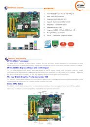
1-1 Feature of Motherboard<br />
• <strong>Intel</strong> <strong>GM45</strong>+ICH9M Series chipset.<br />
• Penyn CPU, with low power consumption never denies high performance.<br />
• Support FSB 1066MHz.<br />
• Support two DDRII SODIMM 800/667MHz up to 4 GB.<br />
• Onboard dual REALTEK RTL 8111C Gigabit Ethernet LAN chip.<br />
• Integrated ALC892 6-channel HD audio CODEC.<br />
• Support USB 2.0 data transport demands.<br />
• Support RS422/485 and watchdog.<br />
• Support GPIO function.<br />
• Support Raid 0, Raid 1 function (only for NF93R).<br />
1
1-2 Specification<br />
Spec<br />
Design<br />
Chipset<br />
CPU<br />
Memory Socket<br />
x Expansion Slots<br />
Integrate IDE<br />
LAN<br />
Audio<br />
BIOS<br />
Multi I/O<br />
Description<br />
∗ Mini ITX form factor 8 layers PCB size: 17.0x17.0cm<br />
∗ <strong>Intel</strong> <strong>GM45</strong>+ICH9M series chipset<br />
∗ Penyn CPU<br />
∗ 200-pin DDRII SO-DIMM slot x2<br />
∗ Support DDRII SODIMM 800/667 MHz system Modules DDRII<br />
SODIMM memory<br />
∗ Expandable to 4GB.<br />
∗ 32-bit PCI slot x 1pcs<br />
∗ Mini PCI-E slot x1pcs<br />
∗ One PCI IDE controller that supports PCI Bus Mastering, ATA<br />
PIO/DMA and the ULTRA DMA 100/66 functions that deliver<br />
the data transfer rate up to 100 MB/s.<br />
∗ Support Raid 0, Raid 1 function(only for NF93R)<br />
∗ Integrated dual Realtek RTL8111C PCI-E Gigabit LAN chip<br />
∗ Support Fast Ethernet LAN function of providing<br />
10Mb/100Mb/1000Mb Ethernet data transfer rate<br />
∗ ALC892 6-channel audio codec integrated<br />
∗ Audio driver and utility included<br />
∗ Award 8MB Flash DIP ROM<br />
∗ HDMI connector x1<br />
∗ DVI-D connector x1<br />
∗ VGA connector x1<br />
∗ RJ-45 LAN connector x2<br />
∗ USB 2.0 port x 4<br />
∗ COM connector x 2<br />
2
1-3 Layout Diagram<br />
∗ Audio connector x1 (Line-in, Line-out, MIC,SPDIF_OUT)<br />
∗ SATAII x4<br />
∗ LVDS header x1<br />
∗ Invert header x1<br />
∗ TV OUT header x1<br />
∗ RS422/RS485 header x1<br />
∗ Front panel header x1<br />
∗ CPUFAN x1 /SYSFAN x2<br />
∗ COM port header x2<br />
∗ USB 2.0 headers x 3 (expandable to 6 x USB 2.0 ports )<br />
∗ GPIO header<br />
∗ PS2 KBMS header x1<br />
∗ IDE hard disk drive header x1<br />
DVI-D<br />
Connector<br />
RJ-45 LAN<br />
Connector<br />
COM<br />
Connector<br />
Line-In/<br />
SPDIF Out<br />
Line-Out<br />
MIC-IN<br />
HDMI<br />
Connector<br />
VGA<br />
Connector<br />
USB<br />
Connector<br />
COM<br />
Connector<br />
3
Inverter Connector<br />
ATX Power Connector<br />
HDMI Connector<br />
CPU Socket<br />
DVI-D Connector<br />
over VGA<br />
Connector<br />
CPU FAN<br />
Header<br />
<strong>Intel</strong> <strong>GM45</strong> Chipset<br />
DDRII<br />
SO-DIMM Slot<br />
RJ-45 LAN over USB<br />
Connectors<br />
RJ-45 LAN over USB<br />
Connectors<br />
LVDS Header<br />
TV OUT Header<br />
<strong>Intel</strong> ICH9M Series<br />
Chipset<br />
SYS FAN1<br />
KBMS Header<br />
IDE Header<br />
COM Connector<br />
Audio Connector<br />
TX-RXCOM4 Header<br />
Mini PCI-E Slot<br />
COM Headers<br />
USB Headers<br />
SATAII Connector<br />
(SATA3,4)<br />
Speaker Header<br />
Front Panel Header<br />
PCI Slot<br />
Front Panel Audio Header<br />
SYS FAN2 Header<br />
SATAII Connector<br />
GPIO Header<br />
(SATA1,2)<br />
4
ALC 892 Audio Chip<br />
Realtek RTL8111C<br />
Gigabit LAN Chip<br />
Realtek RTL8111C<br />
Gigabit LAN Chip<br />
DDRII<br />
SO-DIMM Slot<br />
5
Jumper<br />
Jumper Name Description Page<br />
JBAT CMOS RAM Clear Function Setting 3-pin Block P.8<br />
JP1 Panel Backlight Select 3-pin Block P.8<br />
JP2 Panel VDD Select 3-pin Block P.9<br />
JP3 COM4 RS232/422/485 Function Select 6-pin Block P.9<br />
JP4 COM4 RS232 Power Select 6-pin Block P.10<br />
JP5<br />
Mini PCI-E Power VCC3.3V/3.3V SB 3-pin Block P.10<br />
Power Select<br />
Connectors<br />
Connector Name Description Page<br />
HDMI HDMI port connector 19-pin Connector P.11<br />
VGA-DVI(Bellow) Video Graphic Attach Connector 15-pin Connector P.11<br />
VGA-DVI(Above) DVI-D Port Connector 24-pin Connector P.11<br />
UL1/ UL2<br />
USB Port Connector x4 4-pin Connector P.11<br />
(Middle/Bellow)<br />
UL1/ UL2 (Above) RJ-45 LAN Connector x2 8-pin Connector P.11<br />
COM1 Serial Port Connectors x2 9-pin Connector P.11<br />
AUDIO1 Line-Out /MIC/Line-In Audio Connector 3- Phone Jack P.11<br />
SATA1~4 Serial ATAII Connector 7-pin Connector P.11<br />
6
Headers<br />
Header Name Description Page<br />
AUDIO2 Front Panel Audio Header 9-pin Block P.12<br />
LVDS LVDS Header 32-pin Block P.12<br />
INVERTER1 LVDS Inverter Header 7-pin Block P.14<br />
TV OUT TV Out Header 9-pin Block P.14<br />
TX-RX COM4 RS 422/485 Header 4-pin Block P.15<br />
JW_FP1<br />
(PWR LED/ HD LED/<br />
/Power Button /Reset)<br />
Front Panel Header<br />
(PWR LED/ HD LED/ /Power Button<br />
/Reset)<br />
9-pin Block P.15<br />
CPUFAN,SYSFAN1/2 FAN Speed Headers 3-pin Block P.16<br />
COM3,4 Serial Port COM3/4 Header 9-pin Block P.16<br />
USB1/2/3 USB 2.0 headers 9-pin Block P.17<br />
IO_CON GPIO Header 9-pin Block P.17<br />
KBMS PS/2 Keyboard and mouse Header 6-pin Block P.18<br />
IDE1 IDE Header 44-pin Block P.18<br />
7
Chapter 2<br />
Hardware Installation<br />
2-1 Jumper Setting<br />
(1) JBAT (3-pin): Clear CMOS<br />
JBAT<br />
3<br />
JBAT<br />
3<br />
(2) JP1 (3-pin): Panel Backlights Select<br />
1<br />
1<br />
1-2 closed Normal<br />
2-3 closed Clear CMOS<br />
CMOS RAM Clear Setting<br />
JP1<br />
3<br />
1<br />
1-2 closed <strong>Of</strong>f<br />
JP1<br />
3<br />
1<br />
2-3 closed On<br />
8
(3) JP2 (3-pin): Panel VDD Select<br />
JP2<br />
3<br />
JP2<br />
3<br />
1<br />
1<br />
1-2 closed: 5V<br />
2-3 closed : 3.3V<br />
(4) JP3 (6-pin): COM4 RS232/422/485 Function Select<br />
JP3<br />
1<br />
1<br />
1<br />
1-2 closed: RS232<br />
3-4 closed : RS485<br />
5-6 closed : RS422<br />
9
(5) JP4 (6-pin): COM4 RS232 Power Select<br />
JP4<br />
1<br />
1<br />
1<br />
1-2 closed: RS232<br />
3-4 closed : +12V<br />
5-6 closed : +5V<br />
(6) JP5 (3-pin): Mini PCI-E Power VCC 3.3V/3.3 VSB Function Select<br />
JP5<br />
1<br />
1-2 closed:<br />
Mini PCI-E VCC= +3VSB<br />
3<br />
1 3<br />
2-3 closed:<br />
Mini PCI-E VCC= 3.3V(<br />
10
2-2 Connectors and Headers<br />
2-2-1 Connectors<br />
(1) Audio Connector: (Line-IN/ Line-Out/ MIC-In)<br />
DVI-D<br />
Connector<br />
RJ-45 LAN<br />
Connector<br />
COM<br />
Connector<br />
Line-In/<br />
SPDIF Out<br />
Line-Out<br />
MIC-IN<br />
HDMI<br />
Connector<br />
VGA<br />
Connector<br />
USB<br />
Connector<br />
(2) SATA Port connector: SATA1/SATA2/ SATA3/SATA4<br />
COM<br />
Connector<br />
SATA1<br />
SATA4<br />
SATA3<br />
SATA2<br />
Serial-ATA Connectors<br />
11
2-2-2 Headers<br />
(1) Front Panel Audio (9-pin): AUDIO2<br />
AUDIO2<br />
Pin 1<br />
Lineout2-R<br />
Sense-FB<br />
Lineout2-L<br />
Audio-GND<br />
NC<br />
NC<br />
2<br />
10<br />
9<br />
MIC2-L<br />
MIC2-R<br />
NC<br />
KEY<br />
(2) LVDS Header (32-pin): LVDS<br />
Line-Out, MIC Headers<br />
LVDS Header<br />
Pin 1<br />
Pin 2<br />
12
Pin Pin Definition Pin Pin Definition<br />
Pin 1 LVDSB_DATA3- Pin 2 LVDSB_DATA3+<br />
Pin 3 LVDSB_CLK- Pin 4 LVDSB_CLK+<br />
Pin 5 LVDSB_DATA2- Pin 6 LVDSB_DATA2+<br />
Pin 7 LVDSB_DATA1- Pin 8 LVDSB_DATA1+<br />
Pin 9 LVDSB_DATA0- Pin 10 LVDSB_DATA0+<br />
Pin 11 DDC DATA Pin 12 DDC CLOCK<br />
Pin 13 Ground Pin 14 Ground<br />
Pin 15 Ground Pin 16 Ground<br />
Pin 17 LVDSA_DATA3+ Pin 18 LVDSA_DATA3-<br />
Pin 19 LVDSA_CLK+ Pin 20 LVDSA_CLK-<br />
Pin 21 LVDSA_DATA2+ Pin 22 LVDSA_DATA2-<br />
Pin 23 LVDSA_DATA1+ Pin 24 LVDSA_DATA1-<br />
Pin 25 LVDSA_DATA0+ Pin 26 LVDSA_DATA0-<br />
Pin 27 PVDD Pin 28 PVDD<br />
Pin 29 PVDD Pin 30 PVDD<br />
Pin 31 Ground Pin 32 Ground<br />
13
(3) Pin-headers of LVDS Inverter(7-pin): INVERTER1<br />
Pin 1 and pin2: VCC of inverter<br />
Pin3, pin4 and pin6: GND<br />
Pin5: Backlight<br />
Pin7: Brightness<br />
Brightness<br />
GND<br />
Backlight<br />
GND<br />
GND<br />
+12V<br />
+12V<br />
Pin 1<br />
(4)TV-OUT Header (9-pin): TV_OUT<br />
TV-OUT<br />
NC<br />
Red<br />
Green<br />
NC<br />
Key<br />
10<br />
2<br />
9<br />
Blue<br />
NC<br />
GND<br />
GND<br />
NC<br />
Pin 1<br />
TV-OUT Header<br />
14
(5) RS422/485 Header (4-pin): TX-RXCOM4<br />
RXDP<br />
RXDN<br />
TX-RXCOM4<br />
2<br />
Pin 1<br />
4<br />
3<br />
TXDP<br />
TXDN<br />
RS422/485 Header<br />
(6) Front Panel Header(9-pin): JW_FP1<br />
SPEAK1<br />
Pin 1<br />
SPK-<br />
NC<br />
NC<br />
SPK+<br />
Pin 1<br />
HDLED<br />
HDDLED+<br />
HDDLED-<br />
PWRLED+<br />
PWRLED-<br />
PWR LED<br />
RESET<br />
GND<br />
RSTSW<br />
GND<br />
PWRBTN<br />
PWRBTN<br />
NC<br />
JW _FP1<br />
System Case Connections<br />
15
(7) FAN Speed Headers (3-pin): CPUFAN, SYSFAN1/SYSFAN2<br />
Pin1: GND<br />
Pin2: +12V fan power<br />
Pin3: Fan Speed<br />
CPUFAN<br />
1<br />
3<br />
SYSFAN 1<br />
1 3<br />
SYSFAN2<br />
(8) COM Header (9-pin): COM3/COM4<br />
1<br />
3<br />
COM3/4<br />
RI<br />
CTS<br />
RTS<br />
DSR<br />
GND<br />
DTR<br />
TXD<br />
RX<br />
DCD<br />
5 Pin 1<br />
10<br />
6<br />
COM Header<br />
16
(9) USB 2.0 Port Headers (9-pin): USB1/USB2/ USB3<br />
+5V<br />
-DATA<br />
+DATA<br />
GND<br />
Pi<br />
+5V<br />
-DATA<br />
+DATA<br />
GND<br />
NC<br />
(9) GPIO Header (9-pin): IO_CON<br />
USB 1/2/3 Header<br />
PIN Define PIN Define<br />
1 GPIO_17 6 GPIO_6<br />
2 GPIO_18 7 GPIO_7<br />
GPIO<br />
5<br />
1<br />
3 GPIO_20 8 GPIO_8<br />
10<br />
6<br />
4 GPIO_22 9 GPIO_27<br />
GPIO Header<br />
5 GND 10 KEY<br />
17
(10) KBMS Header (6-pin): KBMS<br />
The header is for PS/2 keyboard and PS/2 Mouse input devices.<br />
MSCLK<br />
+5V<br />
MSDATA<br />
KBDATA<br />
GND<br />
KBCLK<br />
Pin 1<br />
KBMS Header<br />
(11) IDE Header (44-pin):IDE1<br />
IDE1 Header<br />
Pin 2<br />
Pin 1<br />
18
Pin Definition Pin Definition<br />
Pin 1 Reset Pin 2 GND<br />
Pin 3 DD7 Pin 4 DD8<br />
Pin 5 DD6 Pin 6 DD9<br />
Pin 7 DD5 Pin 8 DD10<br />
Pin 9 DD4 Pin 10 DD11<br />
Pin 11 DD3 Pin 12 DD12<br />
Pin 13 DD2 Pin 14 DD13<br />
Pin 15 DD1 Pin 16 DD14<br />
Pin 17 DD0 Pin 18 DD15<br />
Pin 19 GND Pin 20 NC<br />
Pin 21 DMARQ Pin 22 GND<br />
Pin 23 IOW Pin 24 GND<br />
Pin 25 IOR Pin 26 GND<br />
Pin 27 IORDY Pin 28 CSELA<br />
Pin 29 DMACK Pin 30 GND<br />
Pin 31 JINTRQ Pin 32 NC<br />
Pin 33 DA1 Pin 34 PDIAG<br />
Pin 35 DA0 Pin 36 DA2<br />
Pin 37 CS Pin 38 CS1<br />
Pin 39 PRI_ACT Pin 40 GND<br />
Pin 41 +5V Pin 42 +5V<br />
Pin 43 GND Pin 44 NC<br />
19
Attention:<br />
Chapter 3<br />
Introducing BIOS<br />
The BIOS options shown in this manual is for reference use only. We<br />
reserve the right to update the BIOS version without advance notice.<br />
The BIOS is a program located on a Flash Memory on the motherboard. This program is a<br />
bridge between motherboard and operating system. When you start the computer, the BIOS<br />
program will gain control. The BIOS first operates an auto-diagnostic test called POST (power<br />
on self test) for all the necessary hardware, it detects the entire hardware device and<br />
configures the parameters of the hardware synchronization. Only when these tasks are<br />
completed done it gives up control of the computer to operating system (OS). Since the<br />
BIOS is the only channel for hardware and software to communicate, it is the key factor for<br />
system stability, and in ensuring that your system performance as its best.<br />
In the BIOS Setup main menu of Figure 3-1, you can see several options. We will explain<br />
these options step by step in the following pages of this chapter, but let us first see a short<br />
description of the function keys you may use here:<br />
• Press to quit the BIOS Setup.<br />
• Press ↑↓←→ (up, down, left, right) to choose, in the main menu, the option you want<br />
to confirm or to modify.<br />
• Press when you have completed the setup of BIOS parameters to save these<br />
parameters and to exit the BIOS Setup menu.<br />
• Press Page Up/Page Down or +/– keys when you want to modify the BIOS parameters<br />
for the active option.<br />
20
3-1 Entering Setup<br />
Power on the computer and by pressing immediately allows you to enter Setup.<br />
If the message disappears before your respond and you still wish to enter Setup, restart the<br />
system to try again by turning it OFF then ON or pressing the “RESET” button on the system<br />
case. You may also restart by simultaneously pressing , and keys. If<br />
you do not press the keys at the correct time and the system does not boot, an error message<br />
will be displayed and you will again be asked to<br />
Press to continue, or to enter Setup<br />
3-2 Getting Help<br />
Main Menu<br />
The on-line description of the highlighted setup function is displayed at the bottom of the<br />
screen.<br />
Status Page Setup Menu/Option Page Setup Menu<br />
Press F1 to pop up a small help window that describes the appropriate keys to use and the<br />
possible selections for the highlighted item. To exit the Help Window, press .<br />
3-3 The Main Menu<br />
Once you enter Award® BIOS CMOS Setup Utility, the Main Menu (Figure 3-1) will appear<br />
on the screen. The Main Menu allows you to select from fourteen setup functions and two<br />
exit choices. Use arrow keys to select among the items and press to accept or enter<br />
the sub-menu.<br />
21
Phoenix – AwardBIOS CMOS Setup Utility<br />
Standard CMOS Features<br />
Advanced BIOS Features<br />
Advanced Chipset Features<br />
Integrated Peripherals<br />
Power Management Setup<br />
PnP/PCI Configurations<br />
PC Health Status<br />
Load Fail-safe Defaults<br />
Load Optimized Defaults<br />
Set Supervisor Password<br />
Set User Password<br />
Save & Exit Setup<br />
Exit Without Saving<br />
Esc : Quit F9 : Menu in BIOS ↑↓→← : Select Item<br />
F10 : Save & Exit Setup<br />
Figure 3-1<br />
Standard CMOS Features<br />
Use this Menu for basic system configurations.<br />
Advanced BIOS Features<br />
Use this menu to set the Advanced Features available on your system.<br />
Advanced Chipset Features<br />
Use this menu to change the values in the chipset registers and optimize your system’s<br />
performance.<br />
Integrated Peripherals<br />
Use this menu to specify your settings for integrated peripherals.<br />
Power Management Setup<br />
Use this menu to specify your settings for power management.<br />
Miscellaneous Control<br />
22
Use this menu to specify your settings for Miscellaneous Control.<br />
PC Health Status<br />
This entry shows your PC health status.<br />
Power User Overclock Settings<br />
Use this menu to specify your settings (frequency, Voltage) for overclocking demand<br />
CPU Thermal Throttling Setting<br />
The selection is set for activating the active CPU Thermal Protection by flexible CPU loading<br />
adjustment in the arrangement of temperature you defined.<br />
Load Optimized Defaults<br />
Use this menu to load the BIOS default values these are setting for optimal performances system<br />
operations for performance use.<br />
Password Settings<br />
This entry for setting Supervisor password and User password<br />
Save & Exit Setup<br />
Save CMOS value changes to CMOS and exit setup.<br />
Exit Without Saving<br />
Abandon all CMOS value changes and exit setup.<br />
23
3-4 Advanced BIOS Features<br />
Phoenix – AwardBIOS CMOS Setup Utility<br />
Advanced BIOS Features<br />
CPU Feature<br />
Press Enter<br />
Hard Disk Boot Priority<br />
Press Enter<br />
Virus Warning<br />
Disabled<br />
CPU L3 Cache<br />
Enabled<br />
Quick power on self Test<br />
Enabled<br />
First Boot Device<br />
HARD DISK<br />
Second Boot Device<br />
CDROM<br />
Third Boot Device<br />
Disabled<br />
Boot other Device<br />
Enabled<br />
Boot Up NumLock Status<br />
On<br />
Typematic Rate Setting<br />
Disabled<br />
Typematic Rate (Chars/Sec) 6<br />
Typematic Delay (Msec) 250<br />
Security Option<br />
Setup<br />
APIC Mode<br />
Enabled<br />
MPS Version Control For OS 1.4<br />
OS Select For DRAM > 64MB Non-OS2<br />
Report No FDD For WIN 95<br />
Yes<br />
Small Logo(EPA) Show<br />
Disabled<br />
Summary Screen Show<br />
Disabled<br />
Menu Level ><br />
Item Help<br />
↑↓→← Move Enter:Select +/-/PU/PD:Value F10:Save ESC:Exit F1:General Help<br />
F5:Previous Values F6:Optimized Defaults F7:Standard Defaults<br />
Hard Disk Boot Priority<br />
The selection is for you to choose the hard disk drives priorities to boot from.<br />
Virus Warning<br />
The selection Allow you to choose the VIRUS Warning feature for IDE Hard Disk boot sector<br />
protection. If this function is enabled and someone attempt to write data into this area, BIOS<br />
will show a warning message on screen and alarm beep.<br />
24
Disabled (default) No warning message to appear when anything attempts to access the<br />
boot sector or hard disk partition table.<br />
Enabled Activates automatically when the system boots up causing a warning<br />
message to appear when anything attempts to access the boot sector<br />
of hard disk partition table.<br />
CPU Internal Cache<br />
The default value is Enabled.<br />
Enabled (default) Enable cache<br />
Disabled Disable cache<br />
Note: The internal cache is built in the processor.<br />
External Cache<br />
Choose Enabled or Disabled. This option enables the Level 2 cache memory.<br />
Quick Power On Self-Test<br />
This category speeds up Power On Self Test (POST) after you power on the computer. If<br />
this is set to Enabled, BIOS will shorten or skip some check items during POST.<br />
Enabled (default) Enable quick POST<br />
Disabled Normal POST<br />
First/Second/Third Boot Device<br />
The BIOS attempts to load the operating system from the devices in the sequence selected in<br />
these items. The settings are Floppy, LS/ZIP, HDD-0/HDD-1/HDD-3, SCSI, CDROM,<br />
LAD and Disabled.<br />
Boot Up Floppy Seek<br />
During POST, BIOS will determine if the floppy disk drive installed is 40 or 80 tracks.<br />
360K type is 40 tracks while 760K; 1.2M and 1.44M are all 80 tracks.<br />
Boot Up NumLock Status<br />
The default value is on.<br />
On (default) Keypad is numeric keys.<br />
<strong>Of</strong>f Keypad is arrow keys.<br />
Typematic Rate Setting<br />
Keystrokes repeat at a rate determined by the keyboard controller. When enabled, the<br />
typematic rate and typematic delay can be selected. The settings are: Enabled/Disabled.<br />
25
Typematic Rate (Chars/Sec)<br />
Set the number of times a second to repeat a keystroke when you hold the key down. The<br />
settings are: 6, 8, 10, 12, 15, 20, 24, and 30.<br />
Typematic Delay (Msec)<br />
Sets the delay time after the key is held down before beginning to repeat the keystroke. The<br />
settings are 250, 500, 750, and 1000.<br />
Security Option<br />
This category allows you to limit access to the system and Setup, or just to Setup.<br />
System The system will not boot and access to Setup will be denied if the<br />
correct password is not entered at the prompt.<br />
Setup (default) The system will boot, but access to Setup will be denied if the correct<br />
password is not entered prompt.<br />
HDD S.M.A.R.T Capability<br />
This option allow you to enable the HDD S.M.A.R.T Capability (Self-Monitoring, Analysis<br />
and Reporting Technology) . You can choose from Enabled and Disabled.<br />
MPS Version Control For OS 1.4<br />
This option is only valid for multiprocessor motherboards as it specifies the version of the<br />
Multiprocessor Specification (MPS) that the motherboard will use.<br />
OS Select For DRAM > 64MB<br />
Allows OS2® to be used with >64MB or DRAM. Settings are Non-OS/2 (default) and OS2.<br />
Set to OS/2 if using more than 64MB and running OS/2®.<br />
26
3-4-1 CPU Features<br />
C1E Function<br />
Phoenix – AwardBIOS CMOS Setup Utility<br />
CPU Features<br />
Auto<br />
Item Help<br />
CPU C State Capability<br />
Disabled<br />
Execute Disable Bit<br />
Enabled<br />
Menu Level ><br />
Core Multi-Processing<br />
Enabled<br />
↑↓→← Move Enter:Select +/-/PU/PD:Value F10:Save ESC:Exit F1:General Help<br />
F5:Previous Values F6:Optimized Defaults F7:Standard Defaults<br />
3-5 Integrated peripherals<br />
Phoenix – AwardBIOS CMOS Setup Utility<br />
Intergrated peripheral<br />
SIO Device<br />
Press Enter<br />
Onchip IDE Device<br />
Press Enter<br />
Onboard Device<br />
Press Enter<br />
<strong>Intel</strong> Dis Feature<br />
Press Enter<br />
USB Device Setting<br />
Press Enter<br />
RS422/485 Auto Flow Cntr1 Disabled<br />
Power On By Mouse<br />
Disabled<br />
Power On By Keyboard Disabled<br />
Watch Dog set<br />
Disabled<br />
Watch Dog Timer 10<br />
PWRON After PWR-Fail<br />
<strong>Of</strong>f<br />
Item Help<br />
Menu Level >><br />
↑↓→← Move Enter:Select +/-/PU/PD:Value F10:Save ESC:Exit F1:General Help<br />
F5:Previous Values F6:Optimized Defaults F7:Standard Defaults<br />
27
3-5-1 <strong>Intel</strong> DTS Feature<br />
Phoenix – AwardBIOS CMOS Setup Utility<br />
<strong>Intel</strong> DTS Feature<br />
<strong>Intel</strong> DTS Function<br />
Enabled<br />
DTS Active temperature 55℃<br />
Passive Cooling Trip Point 95℃<br />
Passive TC1 Value 2<br />
Passive TC2 Value 0<br />
Passive TSP Value 10<br />
Menu Level ><br />
Item Help<br />
↑↓→← Move Enter:Select +/-/PU/PD:Value F10:Save ESC:Exit F1:General Help<br />
F5:Previous Values F6:Optimized Defaults F7:Standard Defaults<br />
DTS Active Temperature:<br />
This value controls the temperature of the ACPI Active Trip Point- the point in which the os will<br />
turn the CPU on.<br />
NOTE: If the DTS is enabled, only values below 97℃ are valid.<br />
Passive Cooling Trip Point:<br />
This value controls the temperature of the ACPI Active Trip Point- the point in which the os will<br />
begin throttling the CPU.<br />
NOTE: If the DTS is enabled, only values below 97℃ are valid.<br />
Passive TC1 value:<br />
This value sets the TC1 value for the ACPI passive cooling Formula.<br />
Passive TSP Value:<br />
This item sets the TSP value for the ACPI Passive cooling Formula. It represents in tenths of a<br />
second how often the os will read the temperature when Passive Cooling is Enabled.<br />
Critical Trip Point:<br />
28
This value controls the temperature of the ACPI critical Trip point—the point in which the OS<br />
will shut the system off.<br />
NOTES: (1) 100℃ is POP for all the <strong>Intel</strong> CPUS. (2) If value is >100℃ and DTS is enabled,<br />
the Out-of- spec Bit will be used. (3) The value will be set to 127 after ACPI initialization.<br />
Watchdog Timer Select<br />
This item is used to activate the watchdog function. The optional settings are: Enabled; Disabled.<br />
When set it as Enabled user can choose configuration figures in sub items.<br />
Watchdog Timer Value<br />
This item is only activated when Watchdog Timer Select is set as Enabled and users can set a<br />
value from the range of 0~255<br />
*Note: User needs an additional Watchdog Programming Reference Code to make use<br />
of this BIOS function. Detailed procedures please download from our website if<br />
necessary.<br />
29
3-6 PC Health Status<br />
This section shows the Status of you CPU, Fan, and Warning for overall system status. This<br />
is only available if there is Hardware Monitor onboard.<br />
Phoenix – AwardBIOS CMOS Setup Utility<br />
PC Health Status<br />
CPU FAN Configuration<br />
Press Enter<br />
SYS FAN1 Configuration<br />
Press Enter<br />
SYS FAN2 Configuration<br />
Press Enter<br />
Shutdown Temperature<br />
Disabled<br />
VCC 3.3 3.34V<br />
VSB 3.36V<br />
Voltage Battery 3.36V<br />
CPU Temp 42<br />
SYS Temp 47<br />
CPU Fan Speed<br />
6482RPM<br />
SYS1 Fan Speed<br />
0RPM<br />
SYS2 Fan Speed<br />
0RPM<br />
Menu Level ><br />
Item Help<br />
↑↓→← Move Enter:Select +/-/PU/PD:Value F10:Save ESC:Exit F1:General Help<br />
F5:Previous Values F6:Optimized Defaults F7:Standard Defaults<br />
CPU FAN Configurations<br />
CPU Full-Speed Temp<br />
This item allows you setting the FAN works in full speed when the temperature over the value<br />
which out set. If the temperature below the value but over the Idle Temperature, the FAN<br />
will works over 60% of full speed, and the higher temperature will gain higher FAN speed,<br />
after over the temperature which this item setting, the FAN works in full speed.<br />
CPU Idle Temp<br />
This item allows you setting the FAN works in 60% of full speed, when the temperature<br />
lower than the temperature which you setting.<br />
30
3-7 Advanced Chipset Features<br />
The Advanced Chipset Features Setup option is used to change the values of the chipset<br />
registers. These registers control most of the system options in the computer.<br />
Phoenix – AwardBIOS CMOS Setup Utility<br />
Advanced Chipset Features<br />
System BIOS Cacheable<br />
Enabled M<br />
Memory Hole At 15M-16M<br />
Disabled<br />
Vt-d<br />
Disabled<br />
VGA Setting<br />
On-chip Frame Buffer Size<br />
32Mb<br />
Menu Level ><br />
DVMT Mode<br />
Enabled<br />
Total GFX Memory<br />
256MB<br />
PAVP Mode<br />
PAVP-List<br />
VGA Boot Device Setting<br />
Boot Display<br />
VBIOS Default<br />
Panel Scaling<br />
Auto<br />
Panel Type<br />
VBIOS Default<br />
TV1 Standard Type<br />
VBIOS Default<br />
LVDS Switch<br />
Default<br />
CPU Spread Support<br />
Disabled<br />
Spread Mode<br />
Down Spread<br />
↑↓→← Move Enter: Select +/-/PU/PD: Value F10:Save ESC: Exit F1:General Help<br />
F5:Previous Values F6:Optimized Defaults F7:Standard Defaults<br />
System BIOS Cacheable<br />
Selecting Enabled allows caching of the system BIOS ROM at F0000h-FFFFFh, resulting in<br />
better system performance. However, if any program writes to this memory area, a system<br />
error may result. The settings are: Enabled and Disabled.<br />
Total GFX Memory:<br />
For WinXP, the MAX value is base on system memory size 512MB for 1GB DRAM, 768MB<br />
for 1.5GB to 2 GB, 1GB for above 2GB.<br />
31
Boot Display:<br />
Select the video Device that will be activated during POST.<br />
3-8 Power Management Setup<br />
The Power Management Setup allows you to configure your system to most effectively save<br />
energy saving while operating in a manner consistent with your own style of computer use.<br />
Phoenix – AwardBIOS CMOS Setup Utility<br />
Power Management Setup<br />
PCI <strong>Express</strong> PM Function Press Enter<br />
ACPI Suspend Type<br />
Run VGABIOS if S3 Resume<br />
S1(pos)<br />
Auto<br />
Item Help<br />
Power Management<br />
USER Define<br />
Video off Method<br />
Video off Suspend<br />
DPMS<br />
Yes<br />
Menu Level ><br />
Suspend Type<br />
Stop Grant<br />
MODEN USE IRQ 3<br />
Suspend Mode<br />
Disabled<br />
Soft-off by PWR-BTTN<br />
Instant-off<br />
Wake-up by PCI card<br />
Disabled<br />
Power on by ring<br />
Eabled<br />
USB KB Wake up from S3(S4) Disabled<br />
Resume by Alarm<br />
Disabled<br />
Date (of Month) Alarm 0<br />
Time (hh:mm:ss)Alarm 0:0:0<br />
HPET Support<br />
Enabled<br />
HPET Mode<br />
32-bit mde<br />
↑↓→← Move Enter:Select +/-/PU/PD:Value F10:Save ESC:Exit F1:General Help<br />
F5:Previous Values F6:Optimized Defaults F7:Standard Defaults<br />
ACPI Function<br />
This item allows you to Enabled/Disabled the Advanced Configuration and Power<br />
Management (ACPI). The settings are Enabled and Disabled.<br />
Video <strong>Of</strong>f Method<br />
This determines the manner in which the monitor is blanked.<br />
32
DPMS (default) Initial display power management signaling.<br />
Blank Screen This option only writes blanks to the video buffer.<br />
V/H SYNC+Blank This selection will cause the system to turn off the vertical and<br />
horizontal synchronization ports and write blanks to the video buffer.<br />
MODEM Use IRQ<br />
If you want an incoming call on a modem to automatically resume the system from a<br />
power-saving mode, use this item to specify the interrupt request line (IRQ) that is used by<br />
the modem. You might have to connect the fax/modem to the motherboard Wake On Modem<br />
connector for this feature to work.<br />
Soft-<strong>Of</strong>f by PWRBTN<br />
Under ACPI (Advanced Configuration and Power management Interface) you can create a<br />
software power down. In a software power down, the system can be resumed by Wake up<br />
Alarms. This item lets you install a software power down that is controlled by the power<br />
Button on your system. If the item is set to Instant-<strong>Of</strong>f, then the power button causes a<br />
software power down. If the item is set to Delay 4 Sec, then you have to hold the power<br />
button down for four seconds to cause a software power down.<br />
33
3-9 PnP/PCI Configuration<br />
Phoenix – AwardBIOS CMOS Setup Utility<br />
Pnp/PCI Configuration<br />
Init Display First<br />
PCI Slot<br />
Reset Configuration Data<br />
Disabled<br />
Recourse Configuration By<br />
Auto(ESD)<br />
IRQ Recourses<br />
Press Enter<br />
PCI/VGA Palette Snoop<br />
Disabled<br />
INT pin 1 Assignment<br />
Auto<br />
INT pin 2 Assignment<br />
Auto<br />
INT pin 3 Assignment<br />
Auto<br />
INT pin 4 Assignment<br />
Auto<br />
INT pin 5 Assignment<br />
Auto<br />
INT pin 6 Assignment<br />
Auto<br />
INT pin 7 Assignment<br />
Auto<br />
INT pin 8 Assignment<br />
Auto<br />
PCI <strong>Express</strong> relative items<br />
Maximum Payload size 128<br />
Menu Level ><br />
Item Help<br />
↑↓→← Move Enter:Select +/-/PU/PD:Value F10:Save ESC:Exit F1:General Help<br />
F5:Previous Values F6:Optimized Defaults F7:Standard Defaults<br />
34