electron transmission through graphene monolayer-bilayer junction
electron transmission through graphene monolayer-bilayer junction
electron transmission through graphene monolayer-bilayer junction

Create successful ePaper yourself
Turn your PDF publications into a flip-book with our unique Google optimized e-Paper software.
Lithuanian Journal of Physics, Vol. 52, No. 1, pp. 70–80 (2012)<br />
© Lietuvos mokslų akademija, 2012<br />
ELECTRON TRANSMISSION THROUGH GRAPHENE<br />
MONOLAYER-BILAYER JUNCTION: AN ANALYTICAL APPROACH<br />
J. Ruseckas a , A. Mekys a , G. Juzeliūnas a, b , and I. V. Zozoulenko c<br />
a<br />
Institute of Theoretical Physics and Astronomy, Vilnius University, A. Goštauto 12, LT-01108 Vilnius,<br />
Lithuania<br />
E-mail: algirdas.merkys@ff.vu.lt<br />
b<br />
Lithuanian University of Educational Sciences, Studentų 39, LT-08106 Vilnius, Lithuania<br />
c<br />
Solid State Electronics, ITN, Linköping University, 601 74 Norköping, Sweden<br />
Received 30 September 2011; revised 18 December 2011; accepted 1 March 2012<br />
A <strong>junction</strong> of <strong>monolayer</strong> and <strong>bilayer</strong> <strong>graphene</strong> nanoribbons is investigated using the tight-binding approximation.<br />
An external potential is applied on the <strong>bilayer</strong> <strong>graphene</strong> layers to control the <strong>electron</strong>ic transport properties<br />
of the <strong>junction</strong>. The reflection and <strong>transmission</strong> probabilities for an incident <strong>electron</strong> at the <strong>junction</strong> are<br />
analytically calculated. The dependence of the reflection probability on the external potential, the wave vector<br />
of the incident <strong>electron</strong> and the width of the nanoribbon are evaluated.<br />
Keywords: <strong>graphene</strong>, <strong>electron</strong> <strong>transmission</strong><br />
PACS: 81.05.ue<br />
1. Introduction<br />
Graphene is a single sheet of carbon atoms arranged<br />
in a honeycomb lattice. Despite being<br />
a composition part of graphite, a carbon form<br />
known for a long time, <strong>graphene</strong> was isolated only<br />
in 2004. Graphene has attracted scientific interest<br />
because of its unusual <strong>electron</strong>ic and transport<br />
properties that are strikingly different from<br />
those of conventional semiconductor-based twodimensional<br />
<strong>electron</strong>ic systems (for a review see<br />
Refs. [1–4]). The potential impact of this new material<br />
on <strong>electron</strong>ics was immediately recognised.<br />
It has been demonstrated that <strong>graphene</strong> has the<br />
highest carrier mobility at room temperature in<br />
comparison to any other material [5]. However,<br />
<strong>graphene</strong> is a semi-metal with no energy gap and<br />
zero density of states at the Fermi energy. This<br />
makes it difficult to utilise it in <strong>electron</strong>ic devices<br />
such as field effect transistor (FET) requiring<br />
a large on/off current ratio. The energy gap can<br />
be opened in <strong>bilayer</strong> <strong>graphene</strong> by applying a gate<br />
voltage between the layers [6]. This gate-induced<br />
band-gap was demonstrated by Oostinga et al. [7],<br />
and the on/off current ratio of around 100 at room<br />
temperature for a dual-gate <strong>bilayer</strong> <strong>graphene</strong> FET<br />
was reported by IBM [8].<br />
Structures consisting of <strong>graphene</strong> and <strong>bilayer</strong><br />
<strong>graphene</strong> parts can be created by a simple<br />
overlapping of one sheet of <strong>graphene</strong> over the<br />
other. The simplest possible structure containing<br />
<strong>graphene</strong> and <strong>bilayer</strong> <strong>graphene</strong> is a <strong>junction</strong><br />
of these two materials. Due to asymmetry such<br />
<strong>junction</strong> may function in a similar manner to<br />
diode because the conditions for the <strong>electron</strong><br />
to pass the <strong>junction</strong> from the different sides are<br />
not the same. The symmetric structure with two<br />
opposite <strong>junction</strong>s (<strong>graphene</strong>-<strong>bilayer</strong> <strong>graphene</strong><strong>graphene</strong>)<br />
has been already investigated in [9]<br />
using continuum approximation when energy<br />
is close to the Dirac point. External voltage<br />
was applied to control the <strong>electron</strong>ic transport<br />
parameters of the structure. Similar structures<br />
with more different edge geometries were
J. Ruseckas et al. / Lith. J. Phys. 52, 70–80 (2012) 71<br />
investigated in [10]. The investigation was also limited<br />
to the continuum approximation without application<br />
of the external voltage. In our work we use<br />
the tight-binding approximation, which allows us<br />
to investigate the system properties for the whole<br />
energy range. The deficiency of the tight-binding<br />
approximation is the neglection of higher order<br />
corrections, which include the <strong>graphene</strong> nanoribbon<br />
(GNR) bending effect or its conversion into the<br />
nanotube. In this way it becomes indistinguishable<br />
if we have an infinite nanotube with a semi-infinite<br />
nanotube inside or an infinite nanotube is inserted<br />
into another semi-infinite nanotube.<br />
An additional insight into <strong>electron</strong>ic properties<br />
of <strong>graphene</strong> and GNRs can be obtained from exact<br />
analytical approaches. Analytic calculations for the<br />
<strong>electron</strong>ic structure of the GNRs have been reported<br />
in Refs. [11–15]. The <strong>electron</strong>ic structure of <strong>bilayer</strong><br />
<strong>graphene</strong> was addressed in Refs. [16–20] where the<br />
analytical results were presented (both exact and<br />
perturbative). The <strong>electron</strong>ic structure of <strong>bilayer</strong><br />
GNRs was analytically obtained in [21]. A numerical<br />
study of the magnetobandstructure of the GNRs<br />
was reported in Ref. [22, 23], and the numerical<br />
treatment of the edge states in the <strong>bilayer</strong> GNRs was<br />
presented in Ref. [20]. The aim of the present study<br />
is to provide an exact analytical description of the π<br />
<strong>electron</strong> reflection and <strong>transmission</strong> in the <strong>junction</strong><br />
of the <strong>bilayer</strong> and <strong>monolayer</strong> nanoribbons with armchair<br />
edges, with applied external potential.<br />
The paper is organised as follows: in Sec. 2 we<br />
present the known analytical results of <strong>monolayer</strong><br />
and <strong>bilayer</strong> <strong>graphene</strong> and construct the wave function<br />
for the <strong>junction</strong>. Subsequently in Sec. 3 we analyse<br />
the properties of the <strong>electron</strong>ic <strong>transmission</strong><br />
<strong>through</strong> the <strong>junction</strong>. Finally, Sec. 4 summarises<br />
our findings.<br />
2. Analytical expressions of the <strong>electron</strong>ic states<br />
at the <strong>junction</strong><br />
Analytical expressions for the <strong>electron</strong> spectrum<br />
in GNRs and <strong>graphene</strong> nanotubes (GNTs), based<br />
on a tight-binding model, were provided in Ref.<br />
[14] and the expressions for <strong>bilayer</strong> <strong>graphene</strong> were<br />
provided in Ref. [21]. In this section we exploit<br />
these expressions to construct the wave function<br />
for the system of <strong>graphene</strong> connected to <strong>bilayer</strong><br />
<strong>graphene</strong>. One may consider this system as a single<br />
infinite length <strong>graphene</strong> ribbon with another<br />
semi-infinite <strong>graphene</strong> ribbon overlapping, but<br />
mathematically it is simpler to consider the system<br />
as a <strong>junction</strong> of semi-infinite <strong>graphene</strong> with<br />
semi-infinite <strong>bilayer</strong> <strong>graphene</strong> ribbons. For simplicity,<br />
we analyse in this work only AB-α stacking<br />
of <strong>bilayer</strong> <strong>graphene</strong>, as shown in Fig. 1, and other<br />
configurations are left for the future calculations.<br />
Also, the atoms at the <strong>junction</strong> edge are arranged<br />
in a zigzag configuration, while the sides of the<br />
ribbon are in the armchair configuration of the<br />
atoms.<br />
We consider π <strong>electron</strong> spectrum in an infinite<br />
sheet of <strong>graphene</strong>. The structure of <strong>graphene</strong> can<br />
be viewed as a hexagonal lattice with a basis of two<br />
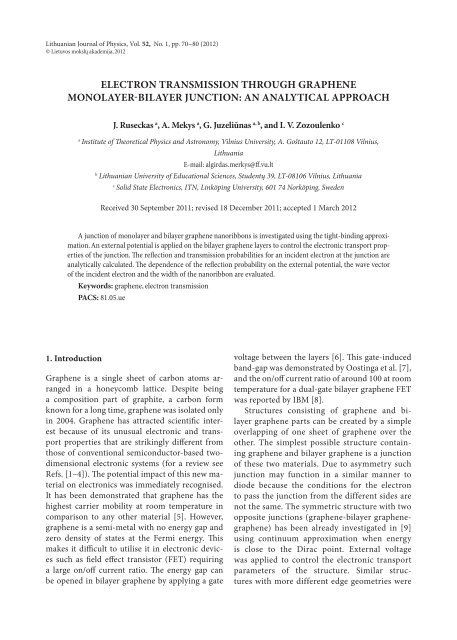
Fig. 1. (Colour online) (a) Sub-lattices A 1<br />
, A 2<br />
, B 1<br />
, B 2<br />
on <strong>bilayer</strong> <strong>graphene</strong> in AB-α stacking. (b) Indication of labels of<br />
carbon atom cells used for <strong>bilayer</strong> <strong>graphene</strong>.
72<br />
J. Ruseckas et al. / Lith. J. Phys. 52, 70–80 (2012)<br />
atoms per unit cell. The Cartesian components of<br />
the lattice vectors a 1<br />
and a 2<br />
are a(³₂, √³₂) and a(³₂,<br />
–√³₂), respectively. Here a ≈ 1.42 is the carboncarbon<br />
distance [1]. The three nearest-neighbour<br />
vectors are given by δ 1<br />
= a(¹₂, √³₂) , δ 2<br />
= a(¹₂,<br />
–√³₂), and δ 3<br />
= a(–1,0). The tight-binding Hamiltonian<br />
for <strong>electron</strong>s in <strong>graphene</strong> has the form<br />
(1)<br />
where the operators a i<br />
and b i<br />
annihilate an <strong>electron</strong><br />
on sub-lattice A at site R i<br />
A<br />
and on sub-lattice<br />
B at site R iB<br />
, respectively (for single <strong>graphene</strong> consider<br />
Fig. 1 with A 1<br />
= A and B 1<br />
= B). The parameter<br />
t is the nearest-neighbour hopping energy<br />
(t ≈ 2.8 eV). Hereinafter all energies will be written<br />
in the units of the hopping integral t, therefore<br />
we set t = 1. Let us label the elementary cells of<br />
the lattice with two numbers p and q. Then the<br />
atoms in the sub-lattices A and B are positioned at<br />
A<br />
B<br />
R p ,q<br />
= pa 1<br />
+ qa 2<br />
and R p ,q<br />
=δ 1<br />
+ pa 1<br />
+ qa 2<br />
respectively.<br />
The π <strong>electron</strong> wave function satisfies the<br />
Schrödinger equation<br />
HΨ = EΨ. (2)<br />
We search for the eigenvectors of the Hamiltonian<br />
(1) in the form of the plane waves (Bloch states) by<br />
taking the probability amplitudes to find an atom<br />
A<br />
B<br />
in the sites R p, ,q<br />
and R p ,q<br />
of the sub-lattices A and<br />
B as<br />
(3)<br />
Thus Eq. (2) yields the eigenvalue equations for<br />
the coefficients c A and c B (envelope functions):<br />
where<br />
–Ec A = c B ϕ˜ (k) , (4)<br />
– Ec B = c A ϕ˜ (–k) , (5)<br />
ϕ˜ (k) ≡ e ik·δ 1 + e ik·δ 2 + e ik·δ 3 . (6)<br />
Further we will consider the spectrum of π <strong>electron</strong>s<br />
in an infinite sheet of <strong>bilayer</strong> <strong>graphene</strong>. The<br />
tight-binding Hamiltonian for <strong>electron</strong>s in <strong>bilayer</strong><br />
<strong>graphene</strong> has the following form:<br />
(7)<br />
where the operators a i, p<br />
and b i, p<br />
annihilate an<br />
<strong>electron</strong> on sub-lattice A p<br />
at site R i<br />
A p<br />
and on sublattice<br />
B p<br />
at site R i<br />
B p<br />
respectively (Fig. 1). The index<br />
p = 1,2 numbers the layers in the <strong>bilayer</strong> system.<br />
In the Hamiltonian (7) we neglected the terms<br />
corresponding to the hopping between atom B 1<br />
and atom B 2<br />
, with the hopping energy γ 3<br />
, and the<br />
terms corresponding to the hopping between atom<br />
A 1<br />
(A 2<br />
) and atom B 2<br />
(B 1<br />
) with the hopping energy<br />
γ 4<br />
. The neglect of these hopping terms leads to the<br />
minimal model of <strong>bilayer</strong> <strong>graphene</strong> [19]. The parameter<br />
t^<br />
(t^≈ 0.4 eV) is the hopping energy between<br />
atom A 1<br />
and atom A 2<br />
while V is half the shift<br />
in the electro-chemical potential between the two<br />
layers. Similarly as in <strong>monolayer</strong> <strong>graphene</strong>, we express<br />
all the energies in the units of t. The atoms in<br />
the sub-lattices A 1<br />
and A 2<br />
are positioned at R p,<br />
A,q 1,2 =<br />
pa 1<br />
+ qa 2<br />
, in the sub-lattice B 1<br />
the aptoms are positioned<br />
at R p<br />
B,q 1 = δ 1<br />
+ pa 1<br />
+ qa 2<br />
and in the sub-lattice<br />
B 2<br />
the atoms are positioned at R p<br />
B,q 2 = –δ 1<br />
+ pa 1<br />
+ qa 2<br />
.<br />
We search for the eigenvectors of the Hamiltonian<br />
(7) in the form of the plane waves. The probability<br />
amplitudes to find an atom in the sites R p,<br />
A,q 1,2 and<br />
R p,<br />
B,q 1,2 of the sub-lattices A j<br />
and A j<br />
are:<br />
(8)<br />
The coefficients (envelope functions) c A p and c B p<br />
obey the eigenvalue equations:<br />
–Ec A 1 = Vc A 1 + c B 1 ϕ˜ (k) + γc A 2<br />
, (9)<br />
–Ec B 1 = Vc B 1 + c A 1 ϕ˜ (–k) , (10)<br />
–Ec A 2 = –Vc A 2 + c B 2 ϕ˜ (–k) + γc A 1<br />
, (11)<br />
–Ec B 2 = –Vc B 2 + c A 2 ϕ˜ (k) . (12)
J. Ruseckas et al. / Lith. J. Phys. 52, 70–80 (2012) 73<br />
Here energy E, potential V, and interaction between<br />
layers γ ≡ t^/t are in the units of the hopping<br />
integral t. Using the nearest-neighbour hopping<br />
energy t ≈ 2.8 eV and the hopping energy between<br />
two layers t^<br />
≈ 0.4 eV, one gets γ ≈ 0.14.<br />
2.1. Electron spectrum in the infinite sheet of<br />
<strong>graphene</strong><br />
Since we are interested in configurations of <strong>graphene</strong><br />
with rectangular geometry, we use a rectangular<br />
unit cell as in Ref. [14] and follow the names<br />
of the variables and functions used in Ref. [21].<br />
Such unit cell has four atoms labelled with symbols<br />
l, λ, ρ, r, as shown in Fig. 1 (consider at this point<br />
only one layer with the labels l 1<br />
, λ 1<br />
, ρ 1<br />
, r 1<br />
, A 1<br />
, B 1<br />
).<br />
The atoms with labels l and ρ belong to the sublattice<br />
A, the atoms with labels λ and r belong to the<br />
sub-lattice B. The position of the unit cell is indicated<br />
with two numbers, n and m. The first Brillouin zone<br />
corresponding to the rectangular unit cell contains<br />
the values of the wave vectors κ, ξ. The eigenvectors<br />
describing the system have the form of plane waves:<br />
The zero energy points have coordinates<br />
in the Brillouin zone corresponding to the rectangular<br />
unit cell.<br />
Since we consider finite-size <strong>graphene</strong> sheets,<br />
evanescent solutions become important. We assume<br />
that exponentially decreasing or increasing<br />
solution can be obtained by taking κ = i|κ| or ξ = i|ξ|<br />
in Eqs. (14), (15) and (17).<br />
2.2. Electron spectrum in the infinite sheet of <strong>bilayer</strong><br />
<strong>graphene</strong><br />
The form of the wave function is similar to <strong>monolayer</strong><br />
<strong>graphene</strong>, Eq. (13), only the labels change:<br />
ψ m,n,αp<br />
(κ, ξ) = c αp<br />
(κ, ξ)e iξm+iκn , (18)<br />
Here the label p = 1, 2 is the number of the layer. The<br />
coefficients of the eigenvectors are (from Ref. [21]):<br />
(19)<br />
ψ m,n,α (κ, ξ) = c α<br />
(κ, ξ)e iξm+iκ , (13)<br />
where α = l, ρ, λ, r.<br />
The coefficients of the eigenvectors are:<br />
(20)<br />
c r<br />
= 1, (14)<br />
(15)<br />
(21)<br />
where<br />
(16)<br />
(22)<br />
and s 3<br />
= ±1 indicates the dispersion branches that<br />
appear due to a smaller Brillouin zone (for more<br />
details see Ref. [21]). The energy is (with s 1<br />
= ±1):<br />
Here s 1<br />
, s 2<br />
= ±1 are the sign coefficients:<br />
(23)<br />
(17)<br />
and the expression for energy is
74<br />
J. Ruseckas et al. / Lith. J. Phys. 52, 70–80 (2012)<br />
(24)<br />
The function ϕ(κ, ξ) has the same expression as<br />
Eq. (16), and V is the electrostatic potential applied<br />
on one layer of <strong>bilayer</strong> <strong>graphene</strong>, while –V is applied<br />
on the other. The parameter γ describes the<br />
interaction between the layers in <strong>bilayer</strong> <strong>graphene</strong>,<br />
γ = 0.14, measured in the same units as energy.<br />
In <strong>bilayer</strong> <strong>graphene</strong> there are two eigenstates<br />
with wave vectors κ (1) and κ (2) , having different absolute<br />
values but corresponding to the same energy:<br />
E (κ (1) , ξ) = E (κ (2) , ξ). One or both of the wave<br />
vectors κ (1) , κ (2) can be imaginary. The energy can be<br />
equal only if the signs s 1<br />
, s 2<br />
obey the condition<br />
we get that |ϕ| 2 is a complex number. This means<br />
that κ is also a complex number and has both real<br />
and imaginary parts.<br />
We have that<br />
(28)<br />
therefore, the dimesnionless x-component of the<br />
wave vector κ can be expressed as<br />
(29)<br />
s 1<br />
(2)<br />
s 2<br />
(2)<br />
= –s 1<br />
(1)<br />
s 2<br />
(1)<br />
. (25)<br />
It has to be noted that the sign coefficients from the<br />
set s 1<br />
, s 2<br />
, s 3<br />
in <strong>bilayer</strong> <strong>graphene</strong> are not necessary,<br />
the same as in the single <strong>graphene</strong> equations.<br />
In addition to the propagating waves, for finitesize<br />
<strong>bilayer</strong> <strong>graphene</strong> sheets evanescent solutions<br />
become important. We assume that exponentially<br />
decreasing or increasing solution can be obtained<br />
by taking κ = i|κ| or ξ = i|ξ|. In addition to the purely<br />
imaginary ξ there are solutions, corresponding to<br />
s 3<br />
= –1, having complex values of ξ.<br />
2.3. Calculation of wave vector from energy<br />
From the dispersion of <strong>bilayer</strong> <strong>graphene</strong> (Eq. (24))<br />
we obtain<br />
The indices s 1<br />
and s 1<br />
can be calculated from the<br />
equations (derived from Eq. (26))<br />
and<br />
(30)<br />
(31)<br />
(26)<br />
From this dispersion equation we find the expression<br />
for |ϕ| 2 :<br />
It should be noted that when<br />
(27)<br />
2.4. Construction of wave functions for the <strong>junction</strong><br />
The <strong>graphene</strong> and <strong>bilayer</strong> <strong>graphene</strong> <strong>junction</strong> is constructed<br />
as shown in Fig. 2. The unit cells (indicated<br />
with two numbers n and m) are the same both<br />
for <strong>graphene</strong> and <strong>bilayer</strong> <strong>graphene</strong>, just starting at<br />
a certain cell n (we choose: n < 0) the upper layer
J. Ruseckas et al. / Lith. J. Phys. 52, 70–80 (2012) 75<br />
Fig. 2. (Colour online) Perspective view of the <strong>graphene</strong>-<strong>bilayer</strong> <strong>graphene</strong> <strong>junction</strong>. The upper layer is connected<br />
to the potential +V, while the lower layer to the potential –V.<br />
of <strong>bilayer</strong> <strong>graphene</strong> is removed. Mathematically the<br />
condition for the absence of the second layer is:<br />
ψ m,n,α2<br />
(κ, ξ) = 0, n < 0. (32)<br />
In particular, at the boundary<br />
ψ m,-1,l2<br />
(κ, ξ) = 0. (33)<br />
The condition for connecting <strong>monolayer</strong> <strong>graphene</strong><br />
and <strong>bilayer</strong> <strong>graphene</strong> solutions is that amplitudes of<br />
<strong>monolayer</strong> and <strong>bilayer</strong> <strong>graphene</strong> should coincide:<br />
ψ m,0,λ<br />
(κ, ξ) = ψ m,0,λ1<br />
(κ, ξ), (34)<br />
The form of the solution in <strong>monolayer</strong> <strong>graphene</strong><br />
then is:<br />
ψ m,n,α<br />
(κ, ξ) = [c α<br />
(ξ j<br />
, κ)eiξ j m –c α<br />
(–ξ j<br />
, κ)e–iξ j m ]e iκn<br />
+ R[c α<br />
(ξ j<br />
, –κ)eiξ j m –c α<br />
(–ξ j<br />
, –κ)e–iξ j m ]e –iκn . (36)<br />
In <strong>bilayer</strong> <strong>graphene</strong> there are two wave vectors κ (1) ,<br />
κ (2) corresponding to the same energy, thus we introduce<br />
two coefficients T 1<br />
and T 2<br />
. The form of the<br />
solution in <strong>bilayer</strong> <strong>graphene</strong> is:<br />
ψ m,n,αp<br />
(κ, ξ) = T 1<br />
[c αp<br />
(ξ j<br />
, κ(1) )e iξ j m –c αp<br />
(–ξ j<br />
, κ (1) )e –iξ j m ]e iκ(1) n<br />
ψ m,0,l<br />
(κ, ξ) = ψ m,0,l1<br />
(κ, ξ). (35)<br />
We analyse the situation when the <strong>electron</strong> approaches<br />
the <strong>junction</strong> from the <strong>graphene</strong> side and<br />
is partially reflected with the reflection probability<br />
|R| 2 . The incoming <strong>electron</strong> wave vector component<br />
κ brings the phase e iκn , while back reflected<br />
it is e –iκn . Since the system is symmetric in the<br />
transverse direction, we construct the combinations<br />
for the wave vector component ξ in the form<br />
(c α<br />
(ξ j<br />
, κ)eiξ j m - c α<br />
(–ξ j<br />
, κ)e–iξ j m ). Here ξ has the index<br />
j for the general case when the discrete values of ξ<br />
are used to describe the finite size system.<br />
+ T 2<br />
[c αp<br />
(ξ j<br />
, κ(2) )e iξ j m – c α p<br />
(–ξ j<br />
, –κ (2) )e –iξ j m ]e –iκ(2) n<br />
. (37)<br />
From the boundary conditions (Eqs. (33)–(35)) we<br />
obtain three equations for three unknowns (R, T 1<br />
and T 2<br />
).<br />
2.5. Reflection and <strong>transmission</strong> amplitudes for<br />
V = 0<br />
In the case when the external potential is zero,<br />
V = 0, by inserting the expressions for the coefficients<br />
from Eqs. (14), (15) and (19)–(22) we get:
76<br />
J. Ruseckas et al. / Lith. J. Phys. 52, 70–80 (2012)<br />
(38)<br />
By inserting the expressions for the coefficients<br />
from Eqs. (44), (45) and (19)–(22) into boundary<br />
conditions we get the equations:<br />
(39)<br />
(46)<br />
(47)<br />
(40)<br />
The solutions are:<br />
(48)<br />
(41)<br />
The solutions for these equations are<br />
(42)<br />
(43)<br />
(49)<br />
2.6. Reflection and <strong>transmission</strong> amplitudes forV> 0<br />
With the potential –V the coefficients of the eigenvectors<br />
in <strong>graphene</strong> are (Ref. [21]):<br />
(44)<br />
(45)<br />
(50)
J. Ruseckas et al. / Lith. J. Phys. 52, 70–80 (2012) 77<br />
The <strong>electron</strong> <strong>transmission</strong> probability|T (κ, ξ j<br />
)| 2 can<br />
be found from the equation<br />
(53)<br />
(51)<br />
where F (κ (1) ,κ (2) , ξ j<br />
) = f (κ (1) , ξ j<br />
)/ f (κ (2) , ξ j<br />
). Further<br />
we are interested in the reflection probability |R| 2 =<br />
|R (κ, ξ j<br />
)| 2 :<br />
(52)<br />
Both coefficients |T(κ, ξ j<br />
)| 2 and |R(κ, ξ j<br />
)| 2 are tied by<br />
the last relation and normalised to unity, thus it is<br />
enough to analyse one of them by meaning that an<br />
increase of reflection causes a decrease of <strong>transmission</strong><br />
and vice versa.<br />
3. Behaviour of reflection probability<br />
3.1. Very large width of nanoribbons<br />
For the infinite (large) width of the <strong>junction</strong> the<br />
wave vector ξ j<br />
values change continuously and the<br />
index j is not required. At first we analyse the dependence<br />
of reflection when ξ is close to the Dirac<br />
point (<br />
). As shown in Fig. 3, the reflection<br />
for every κ at a certain value of the external<br />
potential sharply drops to zero, thus the <strong>junction</strong><br />
becomes transparent for the <strong>electron</strong>s in a certain<br />
state. That state corresponds to the <strong>electron</strong> energy<br />
equal to the potential of the upper layer in <strong>bilayer</strong><br />
<strong>graphene</strong>. Further, with increased potential, reflection<br />
increases to the maximum value and holds in<br />
a relatively wide potential range, then drops again<br />
to the lower values. Thus it is possible to control<br />
reflection (and <strong>transmission</strong>) <strong>through</strong> the barrier<br />
by external potential. The <strong>junction</strong> acts as a tunable<br />
Fig. 3. (a) Dependence of reflection on the wave vector κ and the external potential V. (b) The cut of the graph in<br />
(a) at the potential V = 0.2.
78<br />
J. Ruseckas et al. / Lith. J. Phys. 52, 70–80 (2012)<br />
<strong>electron</strong> spectrum filter: with certain potential we<br />
may pick which energy <strong>electron</strong>s can pass the barrier<br />
without reflection.<br />
3.2. Finite width of nanoribbons<br />
We have a finite number of atoms N in transverse<br />
direction, so the transverse wave vector ξ j<br />
can obtain<br />
only certain values, numbered with the index<br />
j. These values determine the energy subbands. For<br />
the armchair <strong>bilayer</strong> <strong>graphene</strong> ribbon of infinite<br />
length with AB-α stacking, the wave vector ξ j<br />
is determined<br />
by<br />
(54)<br />
In <strong>graphene</strong> and <strong>bilayer</strong> <strong>graphene</strong> nanoribbons<br />
with armchair edges the possible values of the<br />
wave vector ξ j<br />
determine the system conductivity<br />
type, i. e. if there is an energy subband with<br />
the threshold energy coinciding with the chemical<br />
potential (which is set to zero in our investigation),<br />
the conductivity becomes metallic,<br />
otherwise <strong>bilayer</strong> <strong>graphene</strong> appears as semi-conducting.<br />
When V = 0 and j * ≡ 2 (N + 1)/3 is an integer,<br />
then the armchair <strong>bilayer</strong> <strong>graphene</strong> ribbon<br />
is metallic and the index ν = j – j * = 0 corresponds<br />
to the zero-energy band. If 2(N + 1)/3 is not an<br />
integer, the armchair <strong>bilayer</strong> <strong>graphene</strong> ribbon<br />
spectrum has a gap, and the band closest to zero<br />
is either j * ≡ (2N + 1)/3 or j * ≡ (2N + 3)/3 depending<br />
on which of these two numbers is an integer.<br />
Thus the system with N = 100 is semiconducting<br />
and with N = 101 it is metallic. The <strong>electron</strong>ic reflection<br />
(and <strong>transmission</strong>) is also affected by the<br />
width N of the nanoribbons.<br />
By exploiting the relation (54) we show the<br />
dependence of the reflection probability on the<br />
longitudinal wave vector κ and the distance, described<br />
by the index ν, from the zero energy band.<br />
It appears that the reflaction probabilities for<br />
metallic nanoribbons behave similarly as those<br />
for semiconducting nanoribbons, so we show<br />
only one type in Fig. 4. As one can see, when the<br />
wave vector κ is close to zero (corresponding to<br />
the Dirac point), the reflection probability for<br />
the bands with negative and positive indices ν<br />
are the same; this symmetry breaks with increasing<br />
κ. There are values of the external potential<br />
Fig. 4. Dependence of the reflection probability on the<br />
wave vector κ and the subband index ν at different potentials:<br />
(a) V = 0, (b) V = 0.2, (c) V = 1.8.
J. Ruseckas et al. / Lith. J. Phys. 52, 70–80 (2012) 79<br />
where total <strong>transmission</strong> occurs, as can be seen in<br />
Fig. 4(b). In Fig. 4(b) the reflection probability at<br />
certain values of κ and ν drops to zero.<br />
4. Conclusions<br />
An exact analytical description of the <strong>electron</strong>ic<br />
wave function at the <strong>graphene</strong> and AB-α stacking<br />
<strong>bilayer</strong> <strong>graphene</strong> interface based on the tightbinding<br />
model is presented. The model enables to<br />
analyse the properties of the structure far away from<br />
the Dirac point. We investigated the dependence of<br />
probabilities of <strong>electron</strong> reflection and <strong>transmission</strong><br />
<strong>through</strong> the <strong>junction</strong> on the external voltage<br />
in <strong>bilayer</strong> <strong>graphene</strong>. We showed that <strong>transmission</strong><br />
or reflection could be enhanced at certain voltages.<br />
This can be useful for the creation of a transistor<br />
type device from <strong>graphene</strong> nanoribbons. The model<br />
describing the system of the <strong>junction</strong> is suitable for<br />
the extension to other configurations. In addition, a<br />
finite width <strong>graphene</strong> and <strong>bilayer</strong> <strong>graphene</strong> nanoribbon<br />
<strong>junction</strong> was analysed. It was shown that the<br />
size of the ribbon affected the reflection of <strong>electron</strong>s<br />
at the <strong>junction</strong> interface. It was shown that there<br />
was no significant difference of reflection between<br />
metallic and semiconducting <strong>bilayer</strong> <strong>graphene</strong>.<br />
The authors acknowledge a collaborative grant<br />
from the Swedish Institute and a grant No. MIP-<br />
123/2010 by the Research Council of Lithuania.<br />
I.V.Z. acknowledges support from the Swedish Research<br />
Council (VR).<br />
References<br />
[1] A.H.C. Neto, F. Guinea, N.M.R. Peres,<br />
K.S. Novoselov, and A.K. Geim, The <strong>electron</strong>ic properties<br />
of <strong>graphene</strong>, Rev. Mod. Phys. 81, 109 (2009).<br />
[2] D.S.L. Abergela, V. Apalkov, J. Berashevich,<br />
K. Ziegler, and T. Chakraborty, Properties of <strong>graphene</strong>:<br />
a theoretical perspective, Adv. Phys. 59,<br />
261 (2010).<br />
[3] S.D. Sarma, S. Adam, E.H. Hwang, and E. Rossi,<br />
Electronic transport in two-dimensional <strong>graphene</strong>,<br />
Rev. Mod. Phys. 83, 407 (2011).<br />
[4] N.M.R. Peres, Colloquium: The transport properties<br />
of <strong>graphene</strong>: An introduction, Rev. Mod. Phys.<br />
82, 2673 (2010).<br />
[5] X. Du, I. Skachko, A. Barker, and E.Y. Andrei,<br />
Approaching ballistic transport in suspended <strong>graphene</strong>,<br />
Nature Nanotech. 3, 491 (2008).<br />
[6] E. McCann, Asymmetry gap in the <strong>electron</strong>ic band<br />
structure of <strong>bilayer</strong> <strong>graphene</strong>, Phys. Rev. B 74,<br />
161403(R) (2006).<br />
[7] J.B. Oostinga, H.B. Heersche, X. Liu, A.F. Morpurgo,<br />
and L.M.K. Vandersypen, Gate-induced insulating<br />
state in <strong>bilayer</strong> <strong>graphene</strong> devices, Nat. Mat. 7, 151<br />
(2007).<br />
[8] F. Xia, D.B. Farmer, Y. Lin, and P. Avouris,<br />
Graphene feld-effect-transistors with high on / off<br />
current ratio, Nano Lett. 10, 715 (2010).<br />
[9] J. Nilsson, A. Neto, F. Guinea, and N. Peres,<br />
Transmission <strong>through</strong> a biased <strong>graphene</strong> <strong>bilayer</strong><br />
barrier, Phys. Rev. B 76, 165416 (2007).<br />
[10] T. Nakanishi, M. Koshino, and T. Ando,<br />
Transmission <strong>through</strong> a boundary between <strong>monolayer</strong><br />
and <strong>bilayer</strong> <strong>graphene</strong>, Phys. Rev. B 82,<br />
125428 (2010).<br />
[11] L. Brey and H.A. Fertig, Electronic states of <strong>graphene</strong><br />
nanoribbons studied with the Dirac equation,<br />
Phys. Rev. B 73, 235411 (2006).<br />
[12] H. Zheng, Z.F. Wang, T. Luo, Q.W. Shi, and<br />
J. Chen, Analytical study of <strong>electron</strong>ic structure in<br />
armchair <strong>graphene</strong> nanoribbons, Phys. Rev. B 75,<br />
165414 (2007).<br />
[13] L. Malysheva and A.I. Onipko, Spectrum of π <strong>electron</strong>s<br />
in <strong>graphene</strong> as a macromolecule, Phys. Rev.<br />
Lett. 100, 186806 (2008).<br />
[14] A. Onipko, Spectrum of π <strong>electron</strong>s in <strong>graphene</strong><br />
as an alternant macromolecule and its specific features<br />
in quantum conductance, Phys. Rev. B 78,<br />
245412 (2008).<br />
[15] L. Jiang, Y. Zheng, C. Yi, H. Li, and T. Lü, Analytical<br />
study of edge states in a semi-infinite <strong>graphene</strong> nanoribbon,<br />
Phys. Rev. B 80, 155454 (2009).<br />
[16] F. Guinea, A.H.C. Neto, and N.M.R. Peres,<br />
Electronic states and Landau levels in <strong>graphene</strong><br />
stacks, Phys. Rev. B 73, 245426 (2006).<br />
[17] B. Partoens and F.M. Peeters, From <strong>graphene</strong> to<br />
graphite: Electronic structure around the K point,<br />
Phys. Rev. B 74, 075404 (2006).<br />
[18] Z.F. Wang, Q. Li, H. Su, X. Wang, Q.W. Shi,<br />
J. Chen, J. Yang, and J.G. Hou, Electronic structure<br />
of <strong>bilayer</strong> <strong>graphene</strong>: A real-space Green’s function<br />
study, Phys. Rev. B 75, 085424 (2007).<br />
[19] J. Nilsson, A.H.C. Neto, F. Guinea, and N.M.R. Peres,<br />
Electronic properties of <strong>bilayer</strong> and multilayer <strong>graphene</strong>,<br />
Phys. Rev. B 78, 045405 (2008).<br />
[20] E.V. Castro, N.M.R. Peres, J.M.B.L. dos Santos,<br />
A.H.C. Neto, and F. Guinea, Localized States at<br />
zigzag edges of <strong>bilayer</strong> <strong>graphene</strong>, Phys. Rev. Lett.<br />
100, 026802 (2008).<br />
[21] J. Ruseckas, G. Juzeliūnas, and I.V. Zozoulenko,<br />
Spectrum of π <strong>electron</strong>s in <strong>bilayer</strong> <strong>graphene</strong> nanoribbons<br />
and nanotubes: An analytical approach,<br />
Phys. Rev. B 83, 035403 (2011).<br />
[22] H. Xu, T. Heinzel, and I.V. Zozoulenko, Edge disorder<br />
and localization regimes in <strong>bilayer</strong> <strong>graphene</strong><br />
nanoribbons, Phys. Rev. B 80, 045308 (2009).<br />
[23] H. Xu, T. Heinzel, A.A. Shylau, and I.V. Zozoulenko,<br />
Interactions and screening in gated <strong>bilayer</strong> <strong>graphene</strong><br />
nanoribbons, Phys. Rev. B 82, 115311 (2010).
80<br />
J. Ruseckas et al. / Lith. J. Phys. 52, 70–80 (2012)<br />
ELEKTRONŲ PRALAIDUMO GRAFENO IR BIGRAFENO SANDŪROJE<br />
ANALIZINIS ARTINYS<br />
J. Ruseckas a , A. Mekys a , G. Juzeliūnas a, b , I.V. Zozoulenko c<br />
a<br />
Vilniaus universiteto Teorinės fizikos ir astronomijos institutas, Vilnius, Lietuva<br />
b<br />
Lietuvos edukologijos universitetas, Vilnius, Lietuva<br />
c<br />
Linčiopingo universitetas, Norčiopingas, Švedija<br />
Santrauka<br />
Grafenas – tai lakštas, sudarytas iš anglies atomų,<br />
išsidėsčiusių plokštumoje heksagonine struktūra.<br />
Nuo 2004 m. juo susidomėta dėl specifinių elektronų<br />
pernašos savybių. Buvo nustatyta, kad krūvininkų judris<br />
(kambario temperatūroje) jame didžiausias iš visų<br />
iki šiol žinomų medžiagų, o IBM firma jau pademonstravo<br />
veikiantį lauko tranzistorių, pagamintą iš dvigubo<br />
grafeno sluoksnio. Grafenas yra pusmetalis, neturintis<br />
draustinių energijų tarpo, o ties Fermi energija<br />
būsenų tankis lygus nuliui. Draustinių energijų tarpas<br />
yra reikalingas atlikti tranzistoriaus valdymo funkcijas.<br />
Bigrafene šis tarpas sukuriamas prijungus įtampą<br />
tarp sluoksnių, o grafene, pasirodo, jis atsiranda, kai<br />
grafeno lakštas sumažinamas iki nanojuostos matmenų.<br />
Grafeno ir bigrafeno banginės funkcijos jau buvo<br />
suskaičiuotos anksčiau artimo ryšio metodu. Šiame<br />
darbe buvo pasinaudota jau turimais sprendiniais ir<br />
suskaičiuota nauja grafeno ir AB-α konfigūracijos bigrafeno<br />
barjerinės sandūros būsenos funkcija, su kuria<br />
pavyko analiziškai užrašyti elektrono pralaidumo per<br />
sistemą ir atspindžio tikimybes, išreikštas elementariomis<br />
funkcijomis. Ši struktūra yra asimetrinio lauko<br />
tranzistoriaus atitikmuo, kuriame užtūrą sudaro viršutinis<br />
grafeno lakštas bigrafene. Veikiant išoriniu elektriniu<br />
lauku, galima valdyti elektronų pralaidumą per<br />
sistemą. Tokios pat sandaros sitema jau buvo nagrinėta<br />
ir anksčiau, tačiau tik tolydiniu artiniu, o pateikti dėsningumai<br />
nėra pakankamai išanalizuoti. Šiame darbe<br />
suskaičiuota atspindžio tikimybės priklausomybė nuo<br />
išorinio potencialo tarp bigrafeno sluoksnių ir nuo<br />
banginio vektoriaus. Nustatyta, kad potencialui didėjant<br />
atspindys rezonansiškai išauga iki maksimalios<br />
vertės (absoliutaus atspindžio), tada krinta iki minimalios<br />
(absoliutaus pralaidumo), t. y. galima tokią sistemą<br />
valdyti išoriniu potencialu. Taip pat nustatyta, kaip keičiasi<br />
sistemos savybės, kai grafeno ir bigrafeno sandūra<br />
pagaminama ant baigtinio pločio nanojuostos.