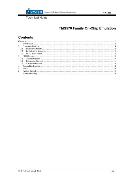
TMS570 Family On-Chip Emulation Contents - iSYSTEM
TMS570 Family On-Chip Emulation Contents - iSYSTEM
TMS570 Family On-Chip Emulation Contents - iSYSTEM

Create successful ePaper yourself
Turn your PDF publications into a flip-book with our unique Google optimized e-Paper software.
_<br />
Technical Notes<br />
V9.7.155<br />
<strong>TMS570</strong> <strong>Family</strong> <strong>On</strong>-<strong>Chip</strong> <strong>Emulation</strong><br />
<strong>Contents</strong><br />
<strong>Contents</strong>................................................................................................................................................................... 1<br />
1 Introduction ..................................................................................................................................................... 2<br />
2 <strong>Emulation</strong> Options........................................................................................................................................... 4<br />
2.1 Hardware Options ..................................................................................................................................... 4<br />
2.2 Initialization Sequence.............................................................................................................................. 6<br />
2.3 JTAG Scan Speed ..................................................................................................................................... 8<br />
3 CPU Options.................................................................................................................................................. 10<br />
3.1 General Options ...................................................................................................................................... 10<br />
3.2 Debugging Options ................................................................................................................................. 11<br />
3.3 Advanced Options................................................................................................................................... 13<br />
4 Access Breakpoints ....................................................................................................................................... 14<br />
5 Trace.............................................................................................................................................................. 14<br />
6 Getting Started............................................................................................................................................... 15<br />
7 Troubleshooting............................................................................................................................................. 19<br />
© <strong>iSYSTEM</strong>, March 2008 1/22
1 Introduction<br />
The JTAG interface offers all basic debug functions, based on which a debugger is implemented in winIDEA:<br />
Read and Write Memory, Read and Write Registers, Run and Stop. Single step is not supported and must be<br />
implemented by the debugger on a higher level. Two hardware breakpoints are available with ARM7, from<br />
which one is usually reserved for source debugging; the other one is available to the user. If the code is loaded<br />
into RAM, an unlimited number of software breakpoints can be set. If software breakpoints are not used, the<br />
second hardware breakpoint can be freed in the Debug/Debug Options/Debugging menu by unchecking the<br />
'Reserve one breakpoint for high level debugging' option.<br />
The ARM7TDMI core-based MCUs include the Debug Communications Channel (DCC). This is a<br />
communication channel implemented into the debug part of the MCU and enables the communication between<br />
the debugger and the MCU. The debugger communicates through the Terminal Window using JTAG, the MCU<br />
on the other side communicates through coprocessor instructions. The communication is alive when the CPU is<br />
in running mode, in stop mode there is no communication.<br />
For more information about the Terminal Window and DCC use please refer to the Software User's Guide,<br />
section 'Debug Session/Terminal Window'.<br />
Debug features:<br />
• Two hardware breakpoints<br />
• Unlimited software breakpoints<br />
• Fast internal/external FLASH programming<br />
• Software flash breakpoints (CPU dependant)<br />
• THUMB support<br />
• Hot Attach<br />
• Real-time memory access through monitor<br />
• Little and big endian support<br />
• <strong>On</strong>-<strong>Chip</strong> Trace<br />
ARM THUMB<br />
The Thumb instruction set is a subset of the most commonly used 32-bit ARM instructions. Thumb instructions<br />
are each 16-bit long and have corresponding 32-bit ARM instruction that has the same effect on the processor<br />
model. Thumb instructions operate with standard ARM register configuration, allowing excellent interoperability<br />
between ARM and Thumb states.<br />
<strong>On</strong> execution, 16-bit Thumb instructions are transparently decompressed to full 32-bit ARM instructions in realtime,<br />
without performance loss.<br />
Thumb code is typically 65% of the size of ARM code and provides 160% of the performance of ARM code<br />
when running on a processor connected to a 16-bit memory system. Thumb therefore is an advantage in<br />
applications with restricted bandwidth, where code density is important. The availability of both 16-bit Thumb<br />
and 32-bit ARM instruction sets gives designers the flexibility to emphasize performance or code size on a<br />
subroutine level, according to the requirements of their applications.<br />
Switching from native ARM 32-bit instruction set to 16-bit Thumb and back represents some overhead for the<br />
application from the aspect of the overall performance. In the real application, the executed Thumb code should<br />
© <strong>iSYSTEM</strong>, March 2008 2/22
e big enough that the increase in performance due to Thumb instruction set use overcomes the loss in<br />
performance due to necessary switch from 32-bit instruction set to Thumb instruction set and switch back to<br />
native 32-bit instruction set at the end of the Thumb code.<br />
THUMB Code Debugging<br />
The debugging can be performed as normal. When the THUMB code is being stepped, the Data in the Code<br />
window is 16-bit long; otherwise it is 32-bit long. Not all CPU registers are available in THUMB mode,<br />
although they can be seen in the SFR window. See the THUMB section of the ARM7 manual for more<br />
information.<br />
Supported CPUs<br />
winIDEA supports all CPUs based on the ARM7DI, ARM7TDMI, ARM720T, ARM920T, ARM922T,<br />
ARM925, ARM926EJS, ARM940T, ARM946ES, ARM966ES, ARM9E and ARM9TDMI cores. Several<br />
microcontrollers have already been implemented, also with special function register (SFR) information. If a<br />
specific microcontroller is not in the CPU list, the core can be selected (i.e. ARM7TDMI, ARM7DI, etc.), the<br />
only backdraw is that the special function registers will not appear. The special function registers can be<br />
implemented for any microcontroller by request, only the SFR specification must be presented. Also custom SFR<br />
definitions can be added, see the Hardware User’s Manual for more information.<br />
Check with <strong>iSYSTEM</strong> for the latest list of supported CPUs.<br />
© <strong>iSYSTEM</strong>, March 2008 3/22
2 <strong>Emulation</strong> Options<br />
2.1 Hardware Options<br />
<strong>Emulation</strong> options, Hardware pane (Debug iCARD)<br />
<strong>Emulation</strong> options, Hardware pane (iTRACE, iTRACE PRO, iTRACE GT)<br />
Debug I/O levels (Debug iCARD)<br />
The development system can be configured in a way that the debug JTAG signals are driven at 3.3V, 5V or<br />
target voltage level (Vref). When 'Vref' Debug I/O level is selected, a voltage applied to the belonging reference<br />
voltage pin on the target debug connector is used as a reference voltage for driving the debug JTAG signals.<br />
Make sure that the target reference voltage pin is connected when 'Vref' Debug I/O level is selected otherwise<br />
the emulation will fail.<br />
© <strong>iSYSTEM</strong>, March 2008 4/22
Sampling and debug threshold levels (iTRACE PRO)<br />
Voltage levels of the debug input and output signals are adjusted depending on the setting.<br />
© <strong>iSYSTEM</strong>, March 2008 5/22
2.2 Initialization Sequence<br />
The user must properly configure the CPU before the debug download (including the flash programming) can<br />
take place to the memory area, which is not accessible upon the CPU reset. This is essential for the applications<br />
using memory resources, for instance external RAM or external flash, which are not accessible after the CPU<br />
reset. In such case, the debugger executes a so-called initialization sequence immediately after the CPU reset,<br />
which writes to the CPU registers configuring the CPU memory interface to the physical memory and then the<br />
debug download is executed. Note that the initialization sequence must be set up specific to the application.<br />
Besides enabling a disabled memory access upon reset, the initialization sequence can also be used for instance<br />
to disable the CPU internal watchdog being active after reset or to modify any other CPU registers, when it’s<br />
preferred to run the application with the modified CPU reset state.<br />
The initialization sequence can be set up in two ways:<br />
1. Set up the initialization sequence by adding necessary register writes directly in the Initialization page<br />
within winIDEA.<br />
2. winIDEA accepts initialization sequence as a text file with .ini extension. The file must be written<br />
according to the syntax specified in the appendix in the hardware user’s guide.<br />
Excerpt from EVB55.ini file for the Atmel AT91M55800 CPU (ARM7TDMI):<br />
S EBI_CSR0 L 0x00402031<br />
S EBI_CSR1 L 0x00802021<br />
S EBI_RCR L 0x00000001<br />
// CS0 - ext. flash, 4 wait states<br />
// CS1 - ext. SRAM<br />
// remap internal RAM<br />
© <strong>iSYSTEM</strong>, March 2008 6/22
The advantage of the second method is that you can simply distribute your .ini file among different workspaces<br />
and users. Additionally, you can easily comment out some line while debugging the initialization sequence itself.<br />
There is also a third method, which can be used too but it’s not highly recommended for the start up. The user<br />
can initialize the CPU by executing part of the code in the target ROM for X seconds by using 'Reset and run for<br />
X sec' option.<br />
© <strong>iSYSTEM</strong>, March 2008 7/22
2.3 JTAG Scan Speed<br />
JTAG Scan Speed definition<br />
Scan speed<br />
The JTAG chain scanning speed can be set to:<br />
• Slow - long delays are introduced in the JTAG scanning to support the slowest devices. JTAG clock<br />
frequency varying from 1 kHz to 2000 kHz can be set.<br />
• Fast – the JTAG chain is scanned with no delays.<br />
• Burst – provides the ability to set the JTAG clock frequency varying from 4 MHz to 100 MHz.<br />
• Burst+ - provides the ability to set the JTAG clock frequency varying from 4 MHz to 100 MHz<br />
• RTCK - Adaptive RTCK clocking for ARM<br />
• Free – this mode is not supported for ARM JTAG debug interface<br />
Slow and Fast JTAG scanning is implemented by means of software toggling the necessary JTAG signals. Burst<br />
mode is a mixture of software and hardware based scanning and should normally work except when the JTAG<br />
scan frequency is an issue that is when the JTAG scan frequency used by the hardware accelerator is too high for<br />
the CPU. In general, selecting an appropriate scan frequency usually depends on scan speed limitations of the<br />
CPU. In Burst+ mode, complete scan is controlled by the hardware accelerator, which poses some preconditions,<br />
which are not met with all CPUs. Consequentially, Burst+ mode doesn’t work for all CPUs. Burst and Burst+ are<br />
not supported on iONE debug tool.<br />
RTCK speed mode is available for ARM family only and is intended for targets which use widely varying<br />
system clock during a debug session. For example, if the CPU switches to different power modes and changes<br />
system clocks, the debugger will be able to maintain synchronization with on-chip debug interface even at much<br />
slower clock. The target CPU needs to provide RTCK synchronization signal, which must be available on pin 11<br />
on standard 20-pin ARM JTAG debug connector. RTCK clock option is available for all development systems<br />
except for older iC3000 ARMx iCARD based development system. Due to extra synchronization, top speed<br />
using "RTCK" mode is about half as fast as "Fast" mode.<br />
© <strong>iSYSTEM</strong>, March 2008 8/22
In general, Fast mode should be used as a default setting. If the debugger works stable with this setting, try Burst<br />
or Burst+ mode to increase the download speed. If Fast mode already fails, try Slow mode at different scan<br />
frequencies until you find a working setting.<br />
Use – Scan Speed during Initialization<br />
<strong>On</strong> some systems, slower scan speed must be used during initialization, during which the CPU clock is raised<br />
(PLL engaged) and then higher scan speeds can be used in operation. In such case, this option and the<br />
appropriate scan speed must be selected.<br />
Configuring JTAG Scan speed for the first time<br />
Sometimes, the default JTAG scan speed needs to be changed. A default ‘Fast’ JTAG scan speed may not work<br />
for all ARM CPUs. WinIDEA may report following message when the debug connection cannot be established<br />
due to too high debug JTAG scan speed:<br />
Select ‘Slow’ JTAG scan speed and try different possible JTAG frequencies when initial debug connection<br />
cannot be established.<br />
Philips LPC2xxx family usually requires ‘Slow’ JTAG scan speed. In general, it is recommended to use the<br />
highest working JTAG scan speed for the optimal debug performance.<br />
© <strong>iSYSTEM</strong>, March 2008 9/22
3 CPU Options<br />
3.1 General Options<br />
Hard Interrupt Disable When Stopped<br />
ARM7 <strong>Family</strong> Debugging Options<br />
When this option is checked interrupts will be enabled immediately after program execution resumes.<br />
Otherwise, the CPU must execute a couple of instructions before returning to the program to determine whether<br />
interrupts were enabled when the CPU was stopped. These extra instruction executions can prevent task<br />
preemption when an interrupt is already pending.<br />
Cache downloaded code only (do not load to target)<br />
When this option is checked, the download files will not propagate to the target using standard debug download<br />
but the Target download files will.<br />
In cases, where the application is previously programmed in the target or it's programmed through the flash<br />
programming dialog, the user may uncheck 'Load code' in the 'Properties' dialog when specifying the debug<br />
download file(s). By doing so, the debugger loads only the necessary debug information for high level<br />
debugging while it doesn't load any code. However, debug functionalities like ETM and Nexus trace will not<br />
work then since an exact code image of the executed code is required as a prerequisite for the correct trace<br />
program flow reconstruction. This applies also for the call stack on some CPU platforms. In such applications,<br />
'Load code' option should remain checked and 'Cache downloaded code only (do not load to target)' option<br />
checked instead. This will yield in debug information and code image loaded to the debugger but no memory<br />
writes will propagate to the target, which otherwise normally load the code to the target.<br />
© <strong>iSYSTEM</strong>, March 2008 10/22
3.2 Debugging Options<br />
Execution Breakpoints<br />
Hardware Breakpoints<br />
ARM7 <strong>Family</strong> Debugging Options<br />
Hardware breakpoints are breakpoints that are already provided by the CPU. The number of hardware<br />
breakpoints is limited to two. The advantage is that they function anywhere in the CPU space, which is not the<br />
case for software breakpoints, which normally cannot be used in the FLASH memory, non-writeable memory<br />
(ROM) or self-modifying code. If the option 'Use hardware breakpoints' is selected, only hardware breakpoints<br />
are used for execution breakpoints.<br />
Note that the debugger, when executing source step debug command, uses one breakpoint. Hence, when all<br />
available hardware breakpoints are used as execution breakpoints, the debugger may fail to execute debug step.<br />
The debugger offers 'Reserve one breakpoint for high-level debugging' option in the Debug/Debug<br />
Options/Debugging' tab to circumvent this. By default this option is checked and the user can uncheck it<br />
anytime.<br />
Software Breakpoints<br />
ARM7 and ARM9 cores provide two hardware breakpoints, which often prove insufficient. The debugger can<br />
use unlimited software breakpoints to work around this limitation.<br />
Note: ARM has no dedicated breakpoint instruction. Instead an invalid op-code is used and one hardware<br />
breakpoint is configured to trigger when this instruction is fetched. Thus only one hardware breakpoint remains<br />
available for hardware execution breakpoints, access breakpoints and trace trigger. If breakpoints are expected to<br />
be set only in areas, where software breakpoints cannot be used, it is advised to turn software breakpoints off,<br />
since this will enable the usage of the hardware breakpoint that is normally reserved.<br />
When a software breakpoint is being used, the program first attempts to modify the source code by placing a<br />
break instruction into the code. If setting software breakpoint fails, a hardware breakpoint is used instead.<br />
Note that the debugger additionally features unlimited software breakpoints in the internal CPU flash for<br />
following families: Philips LPC2000, ST STR7, Atmel AT91SAM7S, Atmel AT91SAM7A and Atmel<br />
AT91SAM7X. Time to set or clear the breakpoint depends on the debug JTAG scan speed, CPU clock and flash<br />
sector size.<br />
© <strong>iSYSTEM</strong>, March 2008 11/22
Simulate instr. step<br />
‘Never’ is selected per default. When run or source step debug command is executed from a BP location, the<br />
debugger first clears BP, executes single step, sets back the original BP and then resumes the application. All this<br />
is done in background hidden from the user. Since setting and clearing software flash breakpoint is time<br />
consuming, a new approach was introduced, which simulates the first instruction at breakpoint address without<br />
requiring clearing and setting the software flash breakpoint. Thereby, the user can select ‘FLASH SW BP’ in<br />
order to speed up the debugging. If the option yields erroneous behavior, set back to the default setting.<br />
Latch target RESET<br />
When the option is checked (default), the debugger latches active target reset until it gets processed. This yields<br />
a delay between the target reset and restart of the application from reset. If this delay is not acceptable for a<br />
specific application, the option should be unchecked. An example is an application where the CPU is<br />
periodically set into a power save mode and then waken up e.g. every 6ms by an external reset circuit. In such<br />
case, a delay introduced by the debugger would yield application not operating properly.<br />
When the option is unchecked, it may happen that the debugger does not detect the target reset although the CPU<br />
gets reset. The debugger polls the CPU status ~3 times per second while the target reset can occur in between.<br />
RESET Duration<br />
The width of the RESET pulse is specified here.<br />
Post RESET Delay<br />
Typically, the on-chip debug module is reset concurrently with the CPU. After the CPU reset line is released<br />
from the active state, the on-chip debug module requires some time (delay) to become operational. The default<br />
delay value normally allows the debugger to gain the control over the CPU. If a first debug connection fails<br />
already try different delay values to establish the debug connection.<br />
© <strong>iSYSTEM</strong>, March 2008 12/22
3.3 Advanced Options<br />
ARM <strong>Family</strong> Advanced options<br />
Override startup register values<br />
This option overrides the default Program Counter reset value with the value set.<br />
Force Supervisor mode while stopped<br />
If this option is checked, Supervisor mode is forced while the application is stopped.<br />
Use Handshaking<br />
When this option is checked, execution of every command is handshaked. This is required by CPUs for which<br />
the JTAG clock is too high.<br />
© <strong>iSYSTEM</strong>, March 2008 13/22
4 Access Breakpoints<br />
ARM Hardware Breakpoints menu<br />
When Breakpoints Occur<br />
A beep can be issued and/or a message displayed indicating that an access breakpoint has occurred.<br />
5 Trace<br />
Please, refer to a separate document describing ARM ETM trace and functionalities based on it.<br />
© <strong>iSYSTEM</strong>, March 2008 14/22
6 Getting Started<br />
Debug Connection<br />
Normally, the minimum settings required by the emulator to be able to connect to the target CPU are specifying<br />
the emulator type, the communication type, the CPU type, specifying the required JTAG speed and specifying<br />
Debug I/O Levels.<br />
• Next, verify if the JTAG connector in the target matches with the pinout defined by the CPU vendor.<br />
The required connector pinout can be also found in the hardware reference document delivered beside<br />
the debug iCARD.<br />
• Connect the emulator to the target.<br />
• First power on the emulator and then the target! When switching off the system, switch off the target<br />
before the emulator!<br />
• Close all debug windows in winIDEA except for the disassembly window.<br />
• Execute debug CPU Reset command.<br />
WinIDEA should display STOP status and disassembly window should display the code around the address<br />
where the program counter points to.<br />
Next step is to download the code in the RAM memory or program the code in the flash.<br />
Before the flash programming or download can take place, the user must ensure that the memory is accessible.<br />
This is very important since there are many applications using memory resources (e.g. external RAM, external<br />
flash), which are not accessible after the CPU reset. In that case, the debugger must execute after the CPU reset a<br />
so called initialization sequence, which configures necessary CPU chip selects and then the download or flash<br />
programming can actually take place. The user must set up the initialization sequence based on his application.<br />
The initialization sequence can be set up in two ways:<br />
1. Set up the initialization sequence by adding necessary register writes directly in the Initialization page<br />
within winIDEA.<br />
© <strong>iSYSTEM</strong>, March 2008 15/22
2. winIDEA accepts initialization sequence as a text file with .ini extension. The file must be written<br />
according to the syntax specified in the appendix in the hardware user’s guide.<br />
Excerpt from EVB55.ini file for the Atmel AT91M55800 CPU (ARM7TDMI):<br />
S EBI_CSR0 L 0x00402031<br />
S EBI_CSR1 L 0x00802021<br />
S EBI_RCR L 0x00000001<br />
// CS0 - ext. flash, 4 wait states<br />
// CS1 - ext. SRAM<br />
// remap internal RAM<br />
The advantage of the second method is that you can simply distribute your .ini file among different workspaces<br />
and users. Additionally, you can easily comment out some line while debugging the initialization sequence itself.<br />
There is also a third method, which can be used too but it’s not highly recommended for the start up. The user<br />
can initialize the CPU by executing part of the code in the target ROM for X seconds by using 'Reset and run for<br />
X sec' option.<br />
© <strong>iSYSTEM</strong>, March 2008 16/22
Debug Download<br />
Debug download is used to load the debug info to the debugger, to load the code in the target RAM memory and<br />
on some CPUs also to load the code in the internal flash (e.g. MAC7100). Otherwise, normally ‘FLASH<br />
Programming Setup’ dialog needs to be invoked to program the flash.<br />
• Specify file(s) to be downloaded in the ‘Debug/Files for download/Download Files’ tab.<br />
• Make sure that ‘Initialize CPU’ before download is configured in the ‘Options’ tab. This yields in the<br />
initialization sequence (explained earlier) being executed before the actual download.<br />
• It’s recommended to check the ‘Verify’ option in the ‘Options’ tab. Then WinIDEA pops up a warning<br />
in case of download error(s).<br />
When debugging the application with the code in the target ROM, it is only necessary to download the debug<br />
info for that memory area. Code can be excluded (click on the file and press ‘Properties’ button). However, if the<br />
file specified here, is used for the flash programming too, then keep the code included and check ‘Cache<br />
downloaded code only (do not load to target)’ option. When this option is checked, memory writes don’t<br />
propagate to the target during debug download. There is also no need for that if there is a flash in the target,<br />
which requires special programming algorithm. In worst case, debug session may even misbehave if memory<br />
writes propagate to the target flash memory during debug download.<br />
© <strong>iSYSTEM</strong>, March 2008 17/22
The debugger should be now operational assuming that the code is loaded in the target RAM or programmed in<br />
the target flash and the debug info loaded to the debugger. The user should be able to reset, run, stop the<br />
application, carry out instruction and source single step, set BPs, etc.<br />
© <strong>iSYSTEM</strong>, March 2008 18/22
7 Troubleshooting<br />
• Try ‘Slow’ JTAG Scan speed if the debugger cannot connect to the CPU.<br />
• Make sure that the power supply is applied to the target JTAG connector when ‘Target VCC’ is selected<br />
for Debug I/O levels in the Hardware/Emulator Options/Hardware tab, otherwise emulation fails or may<br />
behave unpredictably.<br />
• When performing any kind of checksum, remove all software breakpoints since they may impact the<br />
checksum result.<br />
If the ‘Error 175: JTAG chain error. Check target VCC and <strong>Emulation</strong> Options /JTAG Position’ keeps coming<br />
up, it means that the debugger still cannot connect to the ARM <strong>On</strong>-<strong>Chip</strong> debug logic. There are several reasons<br />
possible:<br />
1. the JTAG pins are not connected correctly;<br />
2. there is a problem with power or logical levels of JTAG signals, especially the TCK on the target side must<br />
be checked (if possible on the chip), the signal integrity of, which must be without any problems (without<br />
echoes);<br />
3. the JTAG chain (in the Hardware/<strong>Emulation</strong> Options/JTAG dialog) is not specified correctly. If only one<br />
core and no other scanable device are connected to the JTAG chain, select the 'This is the single device in<br />
the JTAG chain' option (default setting).<br />
Note that the on-chip interrupt logic is not active while the user's program is stopped during the debug session.<br />
© <strong>iSYSTEM</strong>, March 2008 19/22
Notes:<br />
© <strong>iSYSTEM</strong>, March 2008 20/22
Notes:<br />
© <strong>iSYSTEM</strong>, March 2008 21/22
Notes:<br />
Disclaimer: <strong>iSYSTEM</strong> assumes no responsibility for any errors which may appear in this document, reserves the<br />
right to change devices or specifications detailed herein at any time without notice, and does not make any<br />
commitment to update the information herein.<br />
© <strong>iSYSTEM</strong>. All rights reserved.<br />
© <strong>iSYSTEM</strong>, March 2008 22/22