Direct Torque Control with Space Vector Modulation (DTC-SVM) of ...
Direct Torque Control with Space Vector Modulation (DTC-SVM) of ...
Direct Torque Control with Space Vector Modulation (DTC-SVM) of ...

Create successful ePaper yourself
Turn your PDF publications into a flip-book with our unique Google optimized e-Paper software.
Voltage source PWM inverter for PMSM supply<br />
• instate <strong>of</strong> diode rectifier will be use the active rectifier, which provided<br />
controllable DC-link voltage.<br />
• or used bigger capacitor in the DC-link side in order to increase possibility <strong>of</strong><br />
filtering.<br />
Let us summarize, adding influence <strong>of</strong> non-linear VSI causes by:<br />
• serious distortion in the inverter output voltage,<br />
• distorted machine currents,<br />
• torque pulsation,<br />
Additionally, also causes motor instability due to the interaction between motor and the<br />
PWM inverter, or the choice <strong>of</strong> the PWM strategy [25].<br />
Based on simulated and experimental observation one can say that the dead time effect<br />
is:<br />
• more visible in low speed operation <strong>of</strong> the motor,<br />
• may become significantly in drives where high switching frequency is required<br />
for good dynamics performances.<br />
In some applications such as sensor-less vector control, the inverter output voltages are<br />
needed to calculate the rotor or stator flux vectors. Unfortunately, it is very difficult to<br />
measure the output voltage and requires additional hardware. The most desirable<br />
method to obtain the output voltage feedback signal is to use the reference voltages<br />
instead. However, the relation between the output and reference voltage is nonlinear due<br />
to the dead-time effect and voltage drop across power devices. Thus, unless the properly<br />
dead-time and voltage drop compensation will be applied, the reference voltage can not<br />
be used instead <strong>of</strong> the inverter output voltage. Several compensation method were<br />
proposed to overcome this problem. One <strong>of</strong> them will be present bellow.<br />
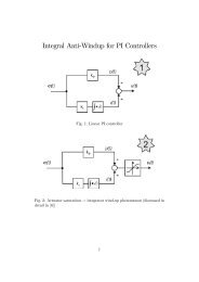
Compensation based on modification <strong>of</strong> reference voltage waveform [17]<br />
The compensation process <strong>of</strong> dead time effect and voltage drop across power devices on<br />
the inverter output voltage from is illustrated in Fig. 3.14.<br />
42


![[TCP] Opis układu - Instytut Sterowania i Elektroniki Przemysłowej ...](https://img.yumpu.com/23535443/1/184x260/tcp-opis-ukladu-instytut-sterowania-i-elektroniki-przemyslowej-.jpg?quality=85)