Direct Torque Control with Space Vector Modulation (DTC-SVM) of ...
Direct Torque Control with Space Vector Modulation (DTC-SVM) of ...
Direct Torque Control with Space Vector Modulation (DTC-SVM) of ...

Create successful ePaper yourself
Turn your PDF publications into a flip-book with our unique Google optimized e-Paper software.
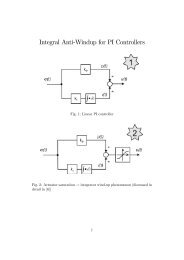
Voltage source PWM inverter for PMSM supply<br />
time”. It guarantees safe operation <strong>of</strong> the inverter. The typical value is from 1µ s - 5µ s .<br />
When the lowest value is for small power IGBT and is growing in respect to increasing<br />
<strong>of</strong> IGBT power. More details about real IGBT module you can find in Appendices.<br />
The effect <strong>of</strong> dead time can be examined from one phase <strong>of</strong> PWM inverter. The basic<br />
configuration is shown in Fig. 3.9. Consist <strong>of</strong> upper and lower power devices T<br />
1<br />
and T<br />
2<br />
,<br />
and reverse recovery diodes D<br />
1<br />
and D<br />
2<br />
, connected between the positive and negative<br />
rails <strong>of</strong> power supply. The gating signals S<br />
A<br />
and S<br />
Ai<br />
come from control block. Output<br />
voltage terminal U<br />
0<br />
is connected to motor phase.<br />
S A<br />
T 1<br />
D 1<br />
U DC<br />
I sA<br />
S Ai<br />
T 2<br />
D 2<br />
LOAD<br />
U 0<br />
S<br />
Dead time<br />
Td<br />
Figure 3.9 Circuit diagram <strong>of</strong> one inverter leg.<br />
Fig. 3.10 shows the ideal control signals and real control signals <strong>with</strong> inserted dead time<br />
T<br />
d<br />
. As can be observed the time duration <strong>of</strong> real drive signal for upper transistor is<br />
shorted than ideal drive signal and for lower transistor is longer than ideal.<br />
Ideal drive signals<br />
Real drive signals<br />
S A<br />
S A<br />
T d<br />
S Ai<br />
S Ai<br />
T d<br />
Figure 3.10 Gate signals control <strong>of</strong> one inverter leg.<br />
39


![[TCP] Opis układu - Instytut Sterowania i Elektroniki Przemysłowej ...](https://img.yumpu.com/23535443/1/184x260/tcp-opis-ukladu-instytut-sterowania-i-elektroniki-przemyslowej-.jpg?quality=85)