Direct Torque Control with Space Vector Modulation (DTC-SVM) of ...
Direct Torque Control with Space Vector Modulation (DTC-SVM) of ...
Direct Torque Control with Space Vector Modulation (DTC-SVM) of ...

You also want an ePaper? Increase the reach of your titles
YUMPU automatically turns print PDFs into web optimized ePapers that Google loves.
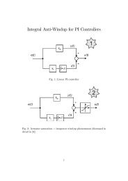
Voltage source PWM inverter for PMSM supply<br />
The one leg <strong>of</strong> inverter consists <strong>of</strong> two transistor switches. A simple transistor switch<br />
consist <strong>of</strong> feedback diode connected in anti-parallel <strong>with</strong> transistor. Feedback diode<br />
conducts current when the load current direction is opposite to the voltage direction.<br />
Assuming that the power devices are ideal: when they are conducting the voltage across<br />
them is zero and they present an open circuit in their blocking mode. Therefore, each<br />
inverter leg can be represented as an ideal switch. Its gives possibility to connect each<br />
<strong>of</strong> the three motor phase coils to a positive or negative voltage <strong>of</strong> the dc link ( U ).<br />
Thus the equivalent scheme for three-phase inverter and possible eight combinations <strong>of</strong><br />
the switches in the inverter are shown in Fig. 3.5.<br />
DC<br />
U<br />
7<br />
= 111<br />
U<br />
0<br />
= 000<br />
U DC<br />
1 1<br />
S<br />
A<br />
SB<br />
1<br />
S C<br />
U DC<br />
S<br />
A<br />
0 0<br />
SB<br />
0<br />
S C<br />
U<br />
1<br />
= 100<br />
A B C<br />
U<br />
2<br />
= 110<br />
A B C<br />
U<br />
3<br />
= 010<br />
U DC<br />
1<br />
SA<br />
0<br />
SB<br />
0<br />
S C<br />
U DC<br />
1 1<br />
S<br />
A<br />
SB<br />
0<br />
S C<br />
U DC<br />
0<br />
S<br />
A<br />
1<br />
SB<br />
0<br />
S C<br />
U<br />
4<br />
= 011<br />
A B C<br />
U<br />
5<br />
= 001<br />
A B C<br />
U<br />
6<br />
= 101<br />
A B C<br />
U DC<br />
0<br />
SA<br />
1<br />
SB<br />
1<br />
S C<br />
U DC<br />
0<br />
S<br />
A<br />
0<br />
SB<br />
1<br />
S C<br />
U DC<br />
1<br />
S<br />
A<br />
0<br />
SB<br />
1<br />
S C<br />
A B C<br />
A B C<br />
A B C<br />
Figure 3.5 Possible switches state in VSI.<br />
The six positions <strong>of</strong> switches ( U1 − U6) produce an output phase voltage equal ± 1/3 or<br />
± 2/3 <strong>of</strong> the DC voltage. The last two ( U0,<br />
U<br />
7) give zero output voltage. The output<br />
phase voltages produced by inverter are shown in Fig. 3.6a. and adequate line to line<br />
voltage calculated in bellow formula also are presented in Fig. 3.6b.<br />
UsAB = UsAN − UsBN<br />
(3.1a)<br />
UsBC = UsBN − UsCN<br />
(3.1b)<br />
UsCA = UsCN − UsAN<br />
(3.1c)<br />
36


![[TCP] Opis układu - Instytut Sterowania i Elektroniki Przemysłowej ...](https://img.yumpu.com/23535443/1/184x260/tcp-opis-ukladu-instytut-sterowania-i-elektroniki-przemyslowej-.jpg?quality=85)