

Application Note AN-1035 - International Rectifier
Application Note AN-1035 - International Rectifier
Application Note AN-1035 - International Rectifier

Create successful ePaper yourself
Turn your PDF publications into a flip-book with our unique Google optimized e-Paper software.
The DirectFET package is designed to have superior<br />
thermal resistance properties. For this reason, it is<br />
essential that the core of the substrate reaches<br />
thermal equilibrium during the pre-heating stage of the<br />
reflow profile to ensure that adequate thermal energy<br />
reaches the solder joint. For more information, visit<br />
www.irf.com/product-info/directfet/dfmanuengineer.html.<br />
Inspection<br />
For comprehensive information on inspecting boardmounted<br />
DirectFET devices, refer to the DirectFET<br />
Inspection <strong>Application</strong> <strong>Note</strong> (<strong>AN</strong>-1080), available at:<br />
www.irf.com/technical-info/appnotes/an-1080.pdf<br />
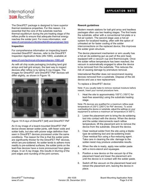
As with all chip scale packaging (including land grid<br />
arrays and ball grid arrays), the best way to inspect<br />
devices after reflow is by taking X-ray images. The<br />
images for DirectFET and DirectFET PbF devices will<br />
differ slightly, as shown in Figure 19.<br />
Figure 19 X-rays of DirectFET (left) and DirectFET PbF<br />
An X-ray image of a board-mounted DirectFET PbF<br />
device shows denser solder joints, with fewer voids and<br />
solder balls, but also with poorer edge definition than<br />
seen in DirectFET devices processed under the same<br />
conditions. The reason for this is that the solder joints<br />
are significantly thicker for the DirectFET PbF devices,<br />
which are pre-soldered. As solder tends to adhere more<br />
readily to pre-soldered surfaces, the solder joints on the<br />
lead-free devices have a more pronounced hour-glass<br />
shape. In an X-ray image, this results in blurring of the<br />
joint edges and rounding of the joint corners.<br />
Rework guidelines<br />
Modern rework stations for ball grid array and leadless<br />
packages often use two heating stages. The first heats<br />
the substrate, either with a conventional hot-plate or a<br />
hot-air system. The second stage uses a hot-air<br />
system for localized heating, often with the option of<br />
unheated air for faster cooling of the solder<br />
interconnections on the replaced device; this improves<br />
the solder grain structure.<br />
The device placement mechanism or arm usually has<br />
a hot-air de-soldering gun as part of the pick head,<br />
equipped with a vacuum cup and thermocouple. Once<br />
the solder reflow temperature has been reached, the<br />
vacuum is automatically engaged to allow the device<br />
to be removed from the substrate. This reduces the<br />
risk of causing damage by premature removal.<br />
<strong>International</strong> <strong>Rectifier</strong> does not recommend reusing<br />
devices removed from a substrate. Dispose of the old<br />
device and use a new replacement.<br />
To replace a DirectFET device:<br />
<strong>Note</strong>: If you usually bake to remove residual moisture before<br />
rework, insert your normal procedure here.<br />
1. Heat the site to approximately 100°C (150°C for<br />
lead-free assembly) using the substrate heating<br />
stage.<br />
<strong>Note</strong>: Pb devices are qualified for a maximum reflow peak<br />
temperature of 230°C (260°C for PbF devices). To avoid<br />
overheating the device or substrate, adjust the settings on your<br />
equipment to achieve a maximum air temperature of 300°C.<br />
2. Lower the placement arm to bring the de-soldering<br />
tool into contact with the device. When the device<br />
and the solder interconnects reach reflow<br />
temperature, lift the placement arm to remove the<br />
device from the substrate. Discard the device.<br />
3. Clear residual solder from the site using a bladetype<br />
de-soldering tool and de-soldering braid.<br />
Clear residual flux using a flux-reducing agent.<br />
Take care in cleaning the site: damage to the<br />
solder-resist may produce undesirable results.<br />
4. When the site is ready, apply new solder paste<br />
with a micro-stencil and squeegee.<br />
5. Position a new device on the vacuum tip of the<br />
placement head and lower the placement arm<br />
until the device is in contact with the solder paste.<br />
6. Switch off the vacuum on the placement head and<br />
retract the placement arm, leaving the device in<br />
place.<br />
DirectFET ® Technology <strong>AN</strong>-<strong>1035</strong> Board Mounting <strong>Application</strong> <strong>Note</strong><br />
www.irf.com Version 26, December 2013 Page 9 of 40


