

Application Note AN-1035 - International Rectifier
Application Note AN-1035 - International Rectifier
Application Note AN-1035 - International Rectifier

You also want an ePaper? Increase the reach of your titles
YUMPU automatically turns print PDFs into web optimized ePapers that Google loves.
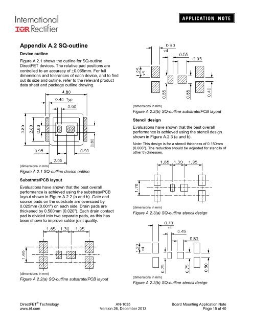
Appendix A.2 SQ-outline<br />
Device outline<br />
Figure A.2.1 shows the outline for SQ-outline<br />
DirectFET devices. The relative pad positions are<br />
controlled to an accuracy of ±0.065mm. For full<br />
dimensions and tolerances of each device, and to find<br />
out its size and outline, refer to the relevant product<br />
data sheet and package outline drawing.<br />
(dimensions in mm)<br />
Figure A.2.2(b) SQ-outline substrate/PCB layout<br />
Stencil design<br />
Evaluations have shown that the best overall<br />
performance is achieved using the stencil design<br />
shown in Figure A.2.3 (a and b).<br />
<strong>Note</strong>: This design is for a stencil thickness of 0.150mm<br />
(0.006"). The reduction should be adjusted for stencils of<br />
other thicknesses.<br />
(dimensions in mm)<br />
Figure A.2.1 SQ-outline device outline<br />
Substrate/PCB layout<br />
Evaluations have shown that the best overall<br />
performance is achieved using the substrate/PCB<br />
layout shown in Figure A.2.2 (a and b). Gate and<br />
source pads on the substrate are oversized by<br />
0.025mm (0.001") on each side. Drain pads are<br />
thickened by 0.500mm (0.020"). Each drain contact<br />
pad is divided into two separate pads, as this has<br />
been shown to improve solder joint quality.<br />
(dimensions in mm)<br />
Figure A.2.3(a) SQ-outline stencil design<br />
(dimensions in mm)<br />
Figure A.2.2(a) SQ-outline substrate/PCB layout<br />
(dimensions in mm)<br />
Figure A.2.3(b) SQ-outline stencil design<br />
DirectFET ® Technology <strong>AN</strong>-<strong>1035</strong> Board Mounting <strong>Application</strong> <strong>Note</strong><br />
www.irf.com Version 26, December 2013 Page 15 of 40


