

Application Note AN-1150 - International Rectifier
Application Note AN-1150 - International Rectifier
Application Note AN-1150 - International Rectifier

Create successful ePaper yourself
Turn your PDF publications into a flip-book with our unique Google optimized e-Paper software.
3.3.3 Dedicated Overvoltage Protection Divider (OVP/EN pin)<br />
In addition to the overvoltage comparator on VFB pin, IR1152 features a 2nd<br />
overvoltage comparator (designated the OVP(OVP) in the IC block diagram)<br />
which is connected to the OVP/EN pin. The OVP(OVP) comparator is identical in<br />
design to the OVP(VFB) comparator and also references the same trigger and<br />
re-enable thresholds of 106% and 103% of V REF respectively. The VFB pin<br />
resistor divider calculated earlier is applicable for the OVP/EN pin also. Hence,<br />
for this converter, 1Mohm, 1% tolerance resistor is selected for R OVP1 & R OVP2<br />
and 26.1kΩ, 1% tolerance resistor is selected for R OVP3 . The trigger and reenable<br />
set-points calculated earlier are likewise applicable here too.<br />
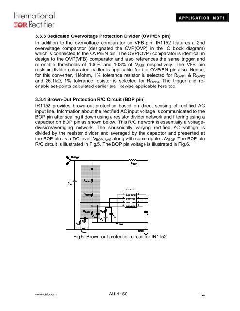
3.3.4 Brown-Out Protection R/C Circuit (BOP pin)<br />
IR1152 provides brown-out protection based on direct sensing of rectified AC<br />
input line. Information about the rectified AC input voltage is communicated to the<br />
BOP pin after scaling it down using a resistor divider network and filtering using a<br />
capacitor on BOP pin as shown below. This R/C network is essentially a voltagedivision/averaging<br />
network. The sinusoidally varying rectified AC voltage is<br />
divided by the resistor divider and averaged by the capacitor and presented at<br />
the BOP pin as a DC level, V BOP, AVG along with some ripple, ∆V BOP . The BOP pin<br />
R/C circuit is illustrated in Fig.5. The BOP pin voltage is illustrated in Fig.6.<br />
Bridge<br />
+<br />
L BST<br />
R BOP1<br />
C IN<br />
R BOP2<br />
R BOP3<br />
IR1152<br />
IR1145<br />
C BOP R gm 1<br />
COM<br />
GATE 8<br />
2<br />
COMP<br />
VCC 7<br />
3<br />
ISNS<br />
VFB 6<br />
4<br />
BOP<br />
OVP/EN 5<br />
C P<br />
C<br />
R SF<br />
C SF<br />
C Z<br />
COM<br />
R SNS<br />
GND<br />
Fig 5: Brown-out protection circuit for IR1152<br />
www.irf.com <strong>AN</strong>-<strong>1150</strong><br />
14


