

24VDC Input Dimmable Electronic Ballast - International Rectifier
24VDC Input Dimmable Electronic Ballast - International Rectifier
24VDC Input Dimmable Electronic Ballast - International Rectifier

Create successful ePaper yourself
Turn your PDF publications into a flip-book with our unique Google optimized e-Paper software.
Presented at<br />
Darnell’s Green Building Power Forum<br />
June 2009<br />
<strong>24VDC</strong> <strong>Input</strong> <strong>Dimmable</strong> <strong>Electronic</strong> <strong>Ballast</strong><br />
Tom Ribarich, John Ribarich, <strong>International</strong> <strong>Rectifier</strong> Corp., USA<br />
Introduction<br />
Solar array installations on building rooftops are becoming more popular as the need for green<br />
energy increases and the cost of solar energy decreases. Since solar arrays output a direct<br />
current this presents a need for electronic devices that can be powered directly from a DC input<br />
instead of the traditional AC input. This paper presents a DC input dimmable electronic ballast<br />
circuit for fluorescent lighting. A new dimming control method is also presented for closed-loop<br />
control of the lamp current over a dimming range of 100% to 10% brightness levels. The final<br />
dimming ballast circuit is built and tested for performance and experimental results are included<br />
to illustrate circuit functionality.<br />
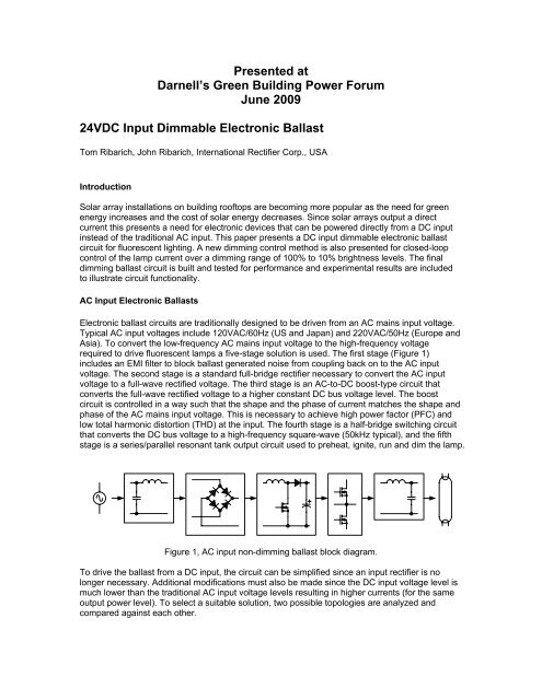
AC <strong>Input</strong> <strong>Electronic</strong> <strong>Ballast</strong>s<br />
<strong>Electronic</strong> ballast circuits are traditionally designed to be driven from an AC mains input voltage.<br />
Typical AC input voltages include 120VAC/60Hz (US and Japan) and 220VAC/50Hz (Europe and<br />
Asia). To convert the low-frequency AC mains input voltage to the high-frequency voltage<br />
required to drive fluorescent lamps a five-stage solution is used. The first stage (Figure 1)<br />
includes an EMI filter to block ballast generated noise from coupling back on to the AC input<br />
voltage. The second stage is a standard full-bridge rectifier necessary to convert the AC input<br />
voltage to a full-wave rectified voltage. The third stage is an AC-to-DC boost-type circuit that<br />
converts the full-wave rectified voltage to a higher constant DC bus voltage level. The boost<br />
circuit is controlled in a way such that the shape and the phase of current matches the shape and<br />
phase of the AC mains input voltage. This is necessary to achieve high power factor (PFC) and<br />
low total harmonic distortion (THD) at the input. The fourth stage is a half-bridge switching circuit<br />
that converts the DC bus voltage to a high-frequency square-wave (50kHz typical), and the fifth<br />
stage is a series/parallel resonant tank output circuit used to preheat, ignite, run and dim the lamp.<br />
Figure 1, AC input non-dimming ballast block diagram.<br />
To drive the ballast from a DC input, the circuit can be simplified since an input rectifier is no<br />
longer necessary. Additional modifications must also be made since the DC input voltage level is<br />
much lower than the traditional AC input voltage levels resulting in higher currents (for the same<br />
output power level). To select a suitable solution, two possible topologies are analyzed and<br />
compared against each other.
DC <strong>Input</strong> <strong>Electronic</strong> <strong>Ballast</strong> Solutions (Boost versus Push-Pull)<br />
Two possible circuit topologies include a boost-type circuit followed by a half-bridge resonant<br />
output stage, or, a push-pull step-up circuit followed by a resonant output stage. The boost<br />
configuration is the same as the AC input solution (Figure 1) except that the rectifier stage can<br />
now be eliminated. The DC input goes to the EMI filter and then directly to the boost stage. The<br />
<strong>24VDC</strong> is then boosted up to a higher DC bus voltage (400VDC) and then converted into a highfrequency<br />
square-wave by the half-bridge switching circuit. The square-wave voltage then feeds<br />
the resonant output circuit that is used to drive the lamp. The push-pull configuration (Figure 2)<br />
uses a step-up transformer to convert the <strong>24VDC</strong> input voltage directly to a high-voltage/highfrequency<br />
square-wave in a single step.<br />
Figure 2, DC input, non-dimming push-pull ballast block diagram.<br />
The boost configuration is similar to the AC input solution, except that the boost converter circuit<br />
has to be re-dimensioned for the higher boost ratio and the power components need to be<br />
rescaled to handle the higher current levels due to the lower input voltage. The boost<br />
configuration has the advantage that the DC bus is regulated to a constant voltage, independent<br />
of the DC input voltage, allowing the circuit to work over a wide range of input voltage. This could<br />
be beneficial when driving the ballast from solar cells since the solar cell output voltage can vary<br />
depending on the outside sunlight level and temperature. The disadvantage of the boost<br />
configuration is the additional cost of the boost circuit, the high voltage rating of the switches, and<br />
the decrease in efficiency due to the additional losses from the boost stage. The push-pull<br />
configuration does the boost and DC-to-AC conversion in a single stage using a step-up<br />
transformer driven by two primary windings. The push-pull configuration has the advantage that<br />
the output is isolated from the input which may or may not be required when driving from solar<br />
cells. The push-pull configuration also has the additional advantages of lower cost due to the<br />
elimination of the boost circuit (but requires a step-up transformer), and lower voltage rated<br />
switches. The disadvantage of the push-pull circuit is that the square-wave voltage feeding the<br />
resonant tank will vary with the DC input voltage level which will limit the input voltage range.<br />
However, the new dimming method described in the next section provides closed-loop control of<br />
the lamp current which will help overcome the dependency on the DC input voltage and widen the<br />
input voltage range. For these reasons, the push-pull configuration has been selected as the<br />
topology to be used for the final ballast design. A comparison of the two topologies has been<br />
summarized in Table I.<br />
New Dimming Control Method<br />
With the push-pull topology selected, the complete dimming design now includes (Figure 3) an<br />
input filter for blocking ballast generated noise, a control IC and push-pull step-up circuit for<br />
producing a high-frequency/high-voltage square-wave voltage, and a resonant output stage for<br />
preheating, igniting and dimming the fluorescent lamp. The additional circuitry needed for<br />
dimming includes (Figure 3) an isolated 0-to-10VDC dimming interface, a current-sensing circuit<br />
to measure the lamp current, and a closed-loop feedback circuit to keep the lamp current<br />
regulated to the user setting by continuously adjusting the output frequency. A closed-loop
system is needed to regulate the lamp current due to the non-linear electrical characteristics of<br />
the fluorescent lamp.<br />
DC <strong>Input</strong> EMI Filter Push-Pull Step-Up Tank Circuit Lamp<br />
+ -<br />
Feedback Current<br />
Frequency<br />
Dimming<br />
Reference<br />
Dimming Circuitry<br />
Sensing<br />
Figure 3, DC input push-pull dimming ballast block diagram.<br />
The new dimming control method includes the lamp current sensing circuit and the closed-loop<br />
feedback circuit. A current sense resistor (RCS) is used to measure the AC lamp current (Figure<br />
4). This AC measurement is then coupled to the DC reference through a feedback capacitor and<br />
resistor (CFB, RFB). The resulting AC+DC signal is then compared to COM and the frequency is<br />
controlled such that the valleys of the AC component are held at COM continuously (Figure 4). If<br />
the DC reference is increased, the valley of the AC+DC signal will increase above COM and the<br />
feedback circuit will decrease the frequency to increase the gain of the resonant tank. This will<br />
increase the lamp current, as well as the amplitude of the AC+DC signal at the DIM pin, until the<br />
valley reaches COM again. If the DC reference is decreased, the valley will decrease below COM.<br />
The feedback circuit will then increase the frequency to decrease the gain of the resonant tank<br />
until the valley reaches COM again. By combining the DC reference with the AC lamp current, a<br />
single node can then be used for both reference and feedback functions to achieve closed-loop<br />
dimming control.<br />
Dimming<br />
Reference and<br />
Feedback<br />
AC Lamp<br />
Current<br />
VREF<br />
VREF<br />
R1<br />
CFB<br />
RFB<br />
VRCS<br />
t<br />
CDIM<br />
RCS<br />
t<br />
VREF+VRCS<br />
VREF100%<br />
VREF10%<br />
t<br />
Figure 4, New AC+DC dimming control method.
To preheat, ignite and dim the lamp, the operating frequency is used as the control parameter.<br />
During preheat and before the lamp ignites, the resonant tank circuit is a series L-C with a high-Q<br />
(Figure 5). During dimming, the resonant tank circuit is a series L, parallel R-C, with a low-Q at<br />
high dimming levels (100%) and a high-Q at low dimming levels (10%).<br />
Vout<br />
Vin<br />
High-Q<br />
Ignition<br />
10%<br />
Preheat<br />
50%<br />
Low-Q<br />
100%<br />
Start<br />
fmin<br />
f100% f50% f10%<br />
fmax<br />
Frequency<br />
Figure 5, Resonant tank Bode plot with dimming operating points.<br />
During preheat, the output frequency starts at a maximum level and is then decreased linearly<br />
(Figure 6). As the frequency decreases, the lamp filaments are preheated by the resonant tank<br />
circulating current. As the frequency decreases further towards the resonance frequency of the<br />
resonant tank circuit the output voltage across the lamp increases. The lamp ignites when the<br />
output voltage exceeds the lamp ignition threshold voltage. Lamp current begins to flow and the<br />
closed-loop feedback circuit controls the lamp current to the desired dimming level.<br />
Figure 6, Preheat, ignition and dimming timing diagram.<br />
30W Dimming <strong>Ballast</strong> Design
The complete schematic is shown in Figure 7. The <strong>24VDC</strong> input voltage first goes<br />
through the EMI filter (CF and LF) followed by the dc bus capacitor (CBUS). The push-pull<br />
switching stage (M1 and M2) is controlled by the IRS2530D IC for preheating, igniting and<br />
dimming the lamp. Resistor RS provides the necessary current for the VCC supply of the IC. The<br />
drains of the push-pull MOSFETs are connected to a centered-tapped primary winding of the<br />
step-up transformer (TSU). The <strong>24VDC</strong> bus is then stepped-up and converted to a highfrequency,<br />
300Vp-p square-wave voltage across the secondary winding, which is used to drive<br />
the resonant output stage. The resonant tank circuit (LRES and CRES) provides the necessary<br />
transfer function for generating high voltages for lamp ignition and low-pass filtering for dimming.<br />
A dc blocking capacitor (CDC) ensures that the lamp current is always AC to prevent mercury<br />
migration which can cause lamp end blackening and a shortened lamp life. Secondary windings<br />
from the resonant inductor (LRES:A,B) and capacitors (CH1 and CH2) are used to heat the lamp<br />
filaments during preheat and dimming. The filament heating circuits also separate the lamp<br />
current from the filament current allowing for a single current-sensing resistor (RCS) to be used to<br />
sense the lamp current. The AC lamp current measurement across RCS is coupled to the DIM<br />
pin through a feedback capacitor and resistor (CFB and RFB). Finally, resistors RSD1 and RSD2<br />
are used to detect if the lamp has been removed and to automatically restart the ballast when the<br />
lamp is re-inserted. Protection against all other ballast fault conditions such as failure to strike,<br />
open filament, and input voltage brown-out, are included internally to the IRS2530D to further<br />
reduce component count and increase reliability.<br />
IRS2530D<br />
Figure 7, Dimming mini-ballast circuit schematic.<br />
The measured ballast waveforms are shown in Figure 6. Figure 6A shows the VCO pin<br />
voltage, lamp voltage and lamp current during normal preheat, ignition and dimming modes. The<br />
VCO pin and lamp voltage ramp up during preheat and ignition to preheat the lamp filaments and<br />
then to ignite the lamp when the lamp ignition voltage threshold is reached. Lamp current starts to<br />
flow immediately after ignition at the start of dimming. Figures 6B and 6C show the half-bridge<br />
output voltage (VS) together with the DIM pin voltage during 100% and 10% dimming conditions.<br />
The DIM pin voltage amplitude decreases (together with the lamp current) from 100% down to
10% and the operating frequency is continuously adjusted to keep the valley of the sinusoid<br />
regulated at COM.<br />
(A)<br />
(B)<br />
(C)<br />
Figure 6, Mini-ballast measured waveforms.<br />
The 0 to 10VDC user dimming input voltage versus the r.m.s. lamp output current (Figure<br />
7) shows good linearity over the entire dimming range.<br />
0.25<br />
0.2<br />
Lamp Current [A]<br />
0.15<br />
0.1<br />
0.05<br />
0<br />
0 1 2 3 4 5 6 7 8 9 10<br />
Dimming <strong>Input</strong> Voltage [VDC]<br />
Figure 7, Dimming input versus lamp current output graph.<br />
Conclusion
<strong>Electronic</strong> ballasts driven off of a DC input have the advantages of no input rectification required<br />
and no PFC stage required. Simplifying the design further using a three-stage push-pull topology<br />
has the additional benefits of eliminating the boost stage to reduce cost, providing isolation, and<br />
increasing lumens/watt. The new closed-loop lamp current control method maintains good<br />
regulation of the lamp current and therefore allows for a wide DC input voltage range without the<br />
need for a constant DC bus voltage. The final ballast design performs well over the complete<br />
input voltage range, including dimming and protection against all fault conditions.<br />
Further improvements to the design for consideration include adding an auxiliary supply for VCC<br />
to achieve a lower DC input voltage level. Also, the same solution can also be used for HID and<br />
LED lighting applications.<br />
References<br />
1) P. Green, AN-1038: Low Voltage DC Supply <strong>Dimmable</strong> <strong>Ballast</strong> for 1x36W Lamp,<br />
http://www.irf.com/technical-info/appnotes/an-1038.pdf.<br />
2) IRS2530D Dimming <strong>Ballast</strong> Control IC, Datasheet, www.irf.com.<br />
3) T. Ribarich, J. Ribarich, A New Model for High-Frequency <strong>Ballast</strong> Design, in IEEE-IAS<br />
Conf. Rec., 1997, pp. 2334-2339.<br />
4) <strong>International</strong> <strong>Rectifier</strong>, IRPLDIM4E and IRPLDIM5E, Reference Design Kits, 2009,<br />
www.irf.com.<br />
5) Elenbaas, W., ed., Fluorescent Lamps, Second Edition, Philips Technical Library,<br />
Eindhoven, The Netherlands 1971.


