

Application Note AN-1077 - International Rectifier
Application Note AN-1077 - International Rectifier
Application Note AN-1077 - International Rectifier

Create successful ePaper yourself
Turn your PDF publications into a flip-book with our unique Google optimized e-Paper software.
<strong>Application</strong> <strong>Note</strong> <strong>AN</strong>-<strong>1077</strong><br />
layer inductor with the same value, but lower interwinding<br />
capacitance is used.<br />
If not controlled this ringing can produce unacceptable<br />
voltages to the sensitive pins of the control<br />
IC, which can disrupt proper circuit operation.<br />
Although an internal blanking circuit is present to<br />
limit the effects of the diode reverse recovery peak on<br />
the current loop, it is recommended to add an RC cell<br />
on the current sense resistor to increase noise immunity<br />
of the control IC.<br />
Another extremely good reason to control the ringing<br />
is to limit the Electro Magnetic Interferences (EMI),<br />
especially in the radiate range<br />
Gate Drive Considerations<br />
The gate driver of the IR1150S is capable of extremely<br />
rapid rise and fall times in addition to the 1.5A<br />
peak source and sink current capability. These rapid<br />
rise and fall capabilities, while providing for an extremely<br />
desirable MosFet drive capacity, can also<br />
create noise issues if not properly controlled.<br />
Often times it is difficult to meet EMI requirements<br />
when drive speeds are too fast resulting in fast rising<br />
dI/dt and dV/dt edges.<br />
This not only taxes the EMI filter, but can introduce<br />
additional noise that the controller is forced to<br />
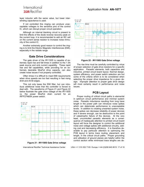
deal with. The waveforms of Figure 21 and Figure 22<br />
below illustrate the gate drive voltage of the IR1150S<br />
vs. the power MosFet drain current for an<br />
IRFP27N60K power switch.<br />
Figure 21 - IR1150S Gate Drive voltage<br />
Figure 22 - IR1150S Gate Drive voltage<br />
The rise time must be carefully controlled by virtue<br />
of proper selection of gate drive resistors for a specific<br />
application. Parasitic elements, both capacitive and<br />
inductive, printed circuit board layout, thermal design,<br />
system efficiency, and power switch selection are but<br />
some of the criteria which is to be considered when<br />
selecting the proper drive impedance for a given design.<br />
Improper attention to proper gate drive design<br />
will most certainly result in performance and noise<br />
issues.<br />
PCB Layout<br />
Proper routing of critical circuit paths is elemental<br />
in optimum circuit performance and minimal system<br />
noise. Parasitic inductance resulting from long trace<br />
length in the power path can introduce noise spikes<br />
which can deteriorate performance to unacceptable<br />
levels. In addition to creating unwanted system noise,<br />
these spikes can decrease reliability of power devices<br />
and if severe enough, can be destructive to the point<br />
of catastrophic failure of the devices. At the very<br />
least, uncontrolled parasitic elements as a consequence<br />
of inadequate attention to printed circuit board<br />
layout will force the designer to control the additional<br />
noise and voltage spikes with additional circuitry, adding<br />
cost and decreasing efficiency. It is therefore desirable<br />
to pay particular attention to optimizing the<br />
PCB layout in terms trace routing, placement, and<br />
length, in the critical circuit paths. Proper grounding<br />
and utilization of ground planes are helpful within the<br />
control section while minimized trace lengths are de-<br />
<strong>International</strong> <strong>Rectifier</strong> Technical Assistance Center: USA ++1 310 252 7105 Europe ++44 (0)208 645 8015 17 of 18


