

Application Note AN-1077 - International Rectifier
Application Note AN-1077 - International Rectifier
Application Note AN-1077 - International Rectifier

Create successful ePaper yourself
Turn your PDF publications into a flip-book with our unique Google optimized e-Paper software.
<strong>Application</strong> <strong>Note</strong> <strong>AN</strong>-<strong>1077</strong><br />
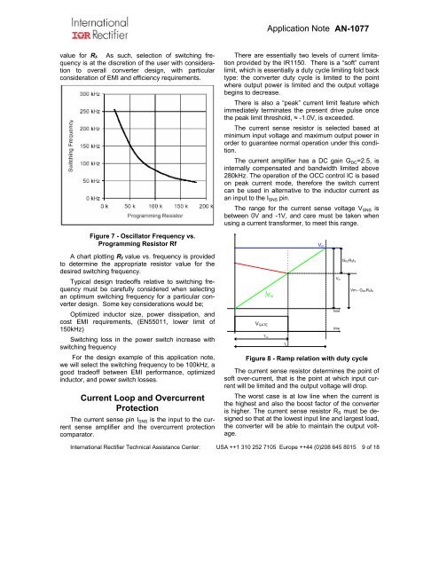
value for R f . As such, selection of switching frequency<br />
is at the discretion of the user with consideration<br />
to overall converter design, with particular<br />
consideration of EMI and efficiency requirements.<br />
Figure 7 - Oscillator Frequency vs.<br />
Programming Resistor Rf<br />
A chart plotting R f value vs. frequency is provided<br />
to determine the appropriate resistor value for the<br />
desired switching frequency.<br />
Typical design tradeoffs relative to switching frequency<br />
must be carefully considered when selecting<br />
an optimum switching frequency for a particular converter<br />
design. Some key considerations would be;<br />
Optimized inductor size, power dissipation, and<br />
cost EMI requirements, (EN55011, lower limit of<br />
150kHz)<br />
Switching loss in the power switch increase with<br />
switching frequency<br />
For the design example of this application note,<br />
we will select the switching frequency to be 100kHz, a<br />
good tradeoff between EMI performance, optimized<br />
inductor, and power switch losses.<br />
Current Loop and Overcurrent<br />
Protection<br />
The current sense pin I SNS is the input to the current<br />
sense amplifier and the overcurrent protection<br />
comparator.<br />
There are essentially two levels of current limitation<br />
provided by the IR1150. There is a “soft” current<br />
limit, which is essentially a duty cycle limiting fold back<br />
type: the converter duty cycle is limited to the point<br />
where output power is limited and the output voltage<br />
begins to decrease.<br />
There is also a “peak” current limit feature which<br />
immediately terminates the present drive pulse once<br />
the peak limit threshold, ≈ -1.0V, is exceeded.<br />
The current sense resistor is selected based at<br />
minimum input voltage and maximum output power in<br />
order to guarantee normal operation under this condition.<br />
The current amplifier has a DC gain G DC =2.5, is<br />
internally compensated and bandwidth limited above<br />
280kHz. The operation of the OCC control IC is based<br />
on peak current mode, therefore the switch current<br />
can be used in alternative to the inductor current as<br />
an input to the I SNS pin.<br />
The range for the current sense voltage V SNS is<br />
between 0V and -1V, and care must be taken when<br />
using a current transformer, to meet this range.<br />
V GATE<br />
Ton<br />
V m<br />
Ts<br />
V m<br />
Vm<br />
time<br />
time<br />
GDCRSIS<br />
Vm - GDCRSIS<br />
Figure 8 - Ramp relation with duty cycle<br />
The current sense resistor determines the point of<br />
soft over-current, that is the point at which input current<br />
will be limited and the output voltage will drop.<br />
The worst case is at low line when the current is<br />
the highest and also the boost factor of the converter<br />
is higher. The current sense resistor R S must be designed<br />
so that at the lowest input line and largest load,<br />
the converter will be able to maintain the output voltage.<br />
<strong>International</strong> <strong>Rectifier</strong> Technical Assistance Center: USA ++1 310 252 7105 Europe ++44 (0)208 645 8015 9 of 18


