

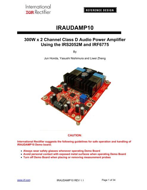
IRAUDAMP10 - International Rectifier
IRAUDAMP10 - International Rectifier
IRAUDAMP10 - International Rectifier

You also want an ePaper? Increase the reach of your titles
YUMPU automatically turns print PDFs into web optimized ePapers that Google loves.
<strong>IRAUDAMP10</strong><br />
300W x 2 Channel Class D Audio Power Amplifier<br />
Using the IRS2052M and IRF6775<br />
By<br />
Jun Honda, Yasushi Nishimura and Liwei Zheng<br />
CAUTION:<br />
<strong>International</strong> <strong>Rectifier</strong> suggests the following guidelines for safe operation and handling of<br />
<strong>IRAUDAMP10</strong> Demo board;<br />
Always wear safety glasses whenever operating Demo Board<br />
Avoid personal contact with exposed metal surfaces when operating Demo Board<br />
Turn off Demo Board when placing or removing measurement probes<br />
www.irf.com Page 1 of 34<br />
<strong>IRAUDAMP10</strong> REV 1.1
TABLE OF CONTENTS<br />
PAGE<br />
INTRODUCTION ............................................................................................................................................... 3<br />
SPECIFICATIONS ............................................................................................................................................ 3<br />
CONNECTION SETUP ..................................................................................................................................... 5<br />
CONNECTOR DESCRIPTION ......................................................................................................................... 5<br />
TEST PROCEDURES ....................................................................................................................................... 6<br />
PERFORMANCE AND TEST GRAPHS .......................................................................................................... 7<br />
SOFT CLIPPING ............................................................................................................................................. 10<br />
EFFICIENCY ................................................................................................................................................... 11<br />
THERMAL CONSIDERATIONS ..................................................................................................................... 11<br />
THERMAL INTERFACE MATERIAL’S PRESSURE CONTROL ................................................................................. 12<br />
POWER SUPPLY REJECTION RATIO (PSRR) ............................................................................................ 14<br />
SHORT CIRCUIT PROTECTION RESPONSE .............................................................................................. 15<br />
<strong>IRAUDAMP10</strong> OVERVIEW ............................................................................................................................ 16<br />
FUNCTIONAL DESCRIPTIONS ..................................................................................................................... 18<br />
IRS2052M GATE DRIVER IC ......................................................................................................................... 18<br />
SELF-OSCILLATING FREQUENCY .................................................................................................................... 19<br />
ADJUSTMENTS OF SELF-OSCILLATING FREQUENCY ......................................................................................... 19<br />
INTERNAL CLOCK OSCILLATOR ....................................................................................................................... 19<br />
SELECTABLE DEAD-TIME ................................................................................................................................ 20<br />
PROTECTION SYSTEM OVERVIEW ............................................................................................................ 21<br />
CLICK AND POP NOISE REDUCTION ......................................................................................................... 23<br />
BUS PUMPING ............................................................................................................................................... 24<br />
INPUT SIGNAL AND GAIN SETTING ........................................................................................................... 24<br />
GAIN SETTING ............................................................................................................................................... 25<br />
<strong>IRAUDAMP10</strong> FABRICATION MATERIALS ................................................................................................. 27<br />
<strong>IRAUDAMP10</strong> PCB SPECIFICATIONS ......................................................................................................... 31<br />
REVISION CHANGES DESCRIPTIONS ........................................................................................................ 34<br />
www.irf.com Page 2 of 34<br />
<strong>IRAUDAMP10</strong> REV 1.1
Introduction<br />
The <strong>IRAUDAMP10</strong> Demo board is a reference design which uses only one IC (IRS2052M) to derive<br />
appropriate input signals, amplify the audio input, and achieve a two-channel 280 W/ch (4Ω, THD+N=1%)<br />
half-bridge Class D audio power amplifier. The reference design demonstrates how to use the IRS2052M<br />
Class D audio controller and gate driver IC, implement protection circuits, and design an optimum PCB<br />
layout using IRF6775 DirectFET MOSFETs. The reference design contains all the required housekeeping<br />
power supplies for ease of use. The two-channel design is scalable, for power and number of channels.<br />
Applications<br />
<br />
<br />
<br />
<br />
<br />
<br />
<br />
AV receivers<br />
Home theater systems<br />
Mini component stereos<br />
Powered speakers<br />
Sub-woofers<br />
Musical Instrument amplifiers<br />
Automotive after market amplifiers<br />
Features<br />
Output Power:<br />
Residual Noise:<br />
Distortion:<br />
Efficiency:<br />
Multiple Protection Features:<br />
PWM Modulator:<br />
300W x 2 channels (4Ω, THD+N=1%)<br />
or 370W x 2 channels (4Ω, THD+N=10%)<br />
220V, IHF-A weighted, AES-17 filter<br />
0.008% THD+N @ 100W, 4Ω<br />
90% @ 300W, 4Ω, single-channel driven, Class D stage<br />
Over-current protection (OCP), high side and low side<br />
Over-voltage protection (OVP),<br />
Under-voltage protection (UVP), high side and low side<br />
Over-temperature protection (OTP)<br />
Self-oscillating half-bridge topology with optional clock synchronization<br />
Specifications<br />
General Test Conditions (unless otherwise noted) Notes / Conditions<br />
Supply Voltages ±50V<br />
Load Impedance<br />
4Ω<br />
Self-Oscillating Frequency 500kHz No input signal, Adjustable<br />
Gain Setting 30.8dB 1Vrms input yields rated power<br />
Electrical Data Typical Notes / Conditions<br />
IR Devices Used<br />
IRS2052M Audio Controller and Gate-Driver,<br />
IRF6775 DirectFET MOSFETs<br />
Modulator<br />
Self-oscillating, second order sigma-delta modulation, analog input<br />
Power Supply Range ± 25V to ±50V Bipolar power supply<br />
Output Power CH1-2: (1% THD+N) 300W 1kHz, ±50V<br />
Output Power CH1-2: (10% THD+N) 370W 1kHz, ±50V<br />
www.irf.com Page 3 of 34<br />
<strong>IRAUDAMP10</strong> REV 1.1
Rated Load Impedance 8-4Ω Resistive load<br />
Standby Supply Current +45/-95mA No input signal<br />
Total Idle Power Consumption 7W No input signal<br />
Channel Efficiency 90% Single-channel driven,<br />
300W, Class D stage<br />
.<br />
Audio Performance<br />
Class D Notes / Conditions<br />
THD+N, 1W<br />
THD+N, 20W<br />
THD+N, 100W<br />
THD+N, 200W<br />
Dynamic Range<br />
Output<br />
0.015%<br />
0.009%<br />
0.008%<br />
0.015%<br />
1kHz, Single-channel driven<br />
100dB<br />
A-weighted, AES-17 filter,<br />
Single-channel operation<br />
Residual Noise, 22Hz - 20kHzAES17 220V Self-oscillating – 500kHz<br />
Damping Factor 51 1kHz, relative to 4Ω load<br />
Channel Separation<br />
74dB<br />
74dB<br />
70dB<br />
100Hz<br />
1kHz<br />
10kHz<br />
Frequency Response : 20Hz-20kHz<br />
: 20Hz-35kHz<br />
±1dB<br />
±3dB<br />
1W, 4Ω - 8Ω Load<br />
Physical Specifications<br />
Dimensions<br />
Weight<br />
3.94”(L) x 2.83”(W) x 0.85”(H)<br />
100 mm (L) x 72 mm (W) x 21.5 mm(H)<br />
0.130kgm<br />
www.irf.com Page 4 of 34<br />
<strong>IRAUDAMP10</strong> REV 1.1
Connection Setup<br />
Fig 1 Typical Test Setup<br />
Connector Description<br />
CN1<br />
P1<br />
P2<br />
P3<br />
Pin # Pin Name Pin Description<br />
1 CH1 INPUT Analog input for CH1<br />
2 GND Floating ground of Channel 1 input<br />
3 GND Floating ground of Channel 2 input<br />
4 CH2 INPUT Analog input for CH2<br />
1 -B -50V supply referenced to GND.<br />
2 GND Ground signal from MB.<br />
3 +B +50V supply referenced to GND.<br />
1 CH2 OUTPUT Output of Channel 2<br />
2 GND Floating ground of Channel 2 output<br />
1 GND Floating ground of Channel 1 output<br />
2 CH1 OUTPUT Output of Channel 1<br />
www.irf.com Page 5 of 34<br />
<strong>IRAUDAMP10</strong> REV 1.1
Test Procedures<br />
Test Setup:<br />
1. Connect 4-200 W dummy loads to 2 output connectors (P2 and P3 as shown on Fig 1)<br />
and an Audio Precision analyzer (AP).<br />
2. Connect the Audio Signal Generator to CN1 for CH1~CH2 respectively (AP).<br />
3. Set up the dual power supply with voltages of ±50V; current limit to 5A.<br />
4. TURN OFF the dual power supply before connecting to On of the unit under test (UUT).<br />
5. Connect the dual power supply to P1. as shown on Fig 1<br />
Power up:<br />
6. Turn ON the dual power supply. The ±B supplies must be applied and removed at the<br />
same time.<br />
7. One orange and two blue LED should turn ON immediately and stay ON<br />
8. Quiescent current for the positive supply should be 45mA 10mA at +50V.<br />
9. Quiescent current for the negative supply should be 95mA 10mA at –50V.<br />
Switching Frequency test<br />
10. With an Oscilloscope, monitor the switching waveform at test points VS1~VS2. Adjust<br />
VR1A and VR1B to set the self oscillating frequency to 500 kHz 25 kHz when DUT in<br />
free oscillating mode.<br />
Functionality Audio Tests:<br />
11. Set the signal generator to 1kHz, 20 mV RMS output.<br />
12. Connect the audio signal generator to CN1(Input of CH1,CH2,CH3)<br />
13. Sweep the audio signal voltage from 15 mV RMS to 1 V RMS .<br />
14. Monitor the output signals at P2/P3 with an oscilloscope. The waveform must be a non<br />
distorted sinusoidal signal.<br />
15. Observe that a 1 V RMS input generates an output voltage of 34.88 V RMS (CH1/CH2). The<br />
ratio, R4x/(R3x) and R30x/(R31x), determines the voltage gain of <strong>IRAUDAMP10</strong>.<br />
Test Setup using Audio Precision (Ap):<br />
16. Use an unbalanced-floating signal from the generator outputs.<br />
17. Use balanced inputs taken across output terminals, P2 and P3.<br />
18. Connect Ap frame ground to GND at terminal P1.<br />
19. Select the AES-17 filter(pull-down menu) for all the testing except frequency response.<br />
20. Use a signal voltage sweep range from 15 mV RMS to 1.5 V RMS .<br />
21. Run Ap test programs for all subsequent tests as shown in Fig 2- Fig 7below.<br />
www.irf.com Page 6 of 34<br />
<strong>IRAUDAMP10</strong> REV 1.1
Performance and test graphs<br />
10<br />
5<br />
2<br />
1<br />
0.5<br />
0.2<br />
%<br />
0.1<br />
0.05<br />
0.02<br />
0.01<br />
0.005<br />
0.002<br />
0.001<br />
100m 200m 500m 1 2 5 10 20 50 100 200 500<br />
W<br />
Sweep Trace Color Line Style Thick Data Axis Com m ent<br />
1 1 Blue Solid 2 Anlr.THD+N Ratio Left CH2<br />
1 3 M agenta Solid 2 Anlr.THD+N Ratio Left CH1<br />
±B Supply = ±50V, 4 Ω Resistive Load<br />
Fig 2 <strong>IRAUDAMP10</strong>, THD+N versus Power, Stereo, 4 Ω<br />
.<br />
+4<br />
+2<br />
T<br />
d<br />
B<br />
r<br />
A<br />
+0<br />
-2<br />
-4<br />
-6<br />
-8<br />
-10<br />
20 50 100 200 500 1k 2k 5k 10k 20k 50k 100k 200k<br />
Hz<br />
Sweep Trace Color Line Style Thick Data Axis Comment<br />
1 1 Blue Solid 2 Anlr.Level B Left CH2<br />
1 2 Magenta Solid 2 Anlr.Level A Left CH1<br />
±B Supply = ±50V, 4 Ω Resistive Load<br />
Fig 3 <strong>IRAUDAMP10</strong>, Frequency response<br />
www.irf.com Page 7 of 34<br />
<strong>IRAUDAMP10</strong> REV 1.1
100<br />
10<br />
1<br />
%<br />
0.1<br />
0.01<br />
0.001<br />
0.0001<br />
20 50 100 200 500 1k 2k 5k 10k 20k<br />
Hz<br />
Sweep Trace Color Line Style Thick Data Axis Comment<br />
1 1 Green Solid 2 Anlr.THD+N Ratio Left 10W<br />
2 1 Yellow Solid 2 Anlr.THD+N Ratio Left 50W<br />
3 1 Red Solid 2 Anlr.THD+N Ratio Left 100W<br />
Fig 4 THD+N Ratio vs. Frequency<br />
+0<br />
-10<br />
-20<br />
-30<br />
-40<br />
d<br />
B<br />
V<br />
-50<br />
-60<br />
-70<br />
-80<br />
-90<br />
-100<br />
-110<br />
10 20 50 100 200 500 1k 2k 5k 10k 20k<br />
Hz<br />
Sweep Trace Color Line Style Thick Data Axis Comment<br />
1 1 Blue Solid 2 Fft.Ch.1 Ampl Left CH2<br />
1 2 Magenta Solid 2 Fft.Ch.2 Ampl Left CH1<br />
Fig 5, 1V output Frequency Spectrum<br />
www.irf.com Page 8 of 34<br />
<strong>IRAUDAMP10</strong> REV 1.1
+20<br />
+0<br />
-20<br />
d<br />
B<br />
V<br />
-40<br />
-60<br />
-80<br />
-100<br />
-120<br />
-140<br />
10 20 50 100 200 500 1k 2k 5k 10k 20k<br />
Hz<br />
Sweep Trace Color Line Style Thick Data Axis Comment<br />
1 1 Blue Solid 2 Fft.Ch.1 Ampl Left CH2<br />
1 2 Magenta Solid 2 Fft.Ch.2 Ampl Left CH1<br />
No signal, Self Oscillator @ 500kHz<br />
Fig 6, <strong>IRAUDAMP10</strong> Noise Floor<br />
.<br />
+0<br />
-10<br />
-20<br />
-30<br />
d<br />
B<br />
r<br />
A<br />
-40<br />
-50<br />
-60<br />
-70<br />
-80<br />
-90<br />
-100<br />
20 50 100 200 500 1k 2k 5k 10k 20k<br />
Hz<br />
Sweep Trace Color Line Style Thick Data Axis Comment<br />
1 1 Blue Solid 2 Anlr.Ampl Left CH2-CH1<br />
1 2 Magenta Solid 2 Anlr.Ampl Left CH1-CH2<br />
Fig 7, Channel separation vs. frequency<br />
.<br />
www.irf.com Page 9 of 34<br />
<strong>IRAUDAMP10</strong> REV 1.1
Soft Clipping<br />
IRS2052M has Clipping detection function, it monitors error voltage in COMP pin with a window<br />
comparator and pull an open drain nmos referenced to GND. Threshold to detect is at 10% and<br />
90% of VAA-VSS. Each channel has independent CLIP outputs. Once IRS2052M detects<br />
Clipping, the CLIP pin can generate pulses to trigger soft clipping circuit, which can limit output’s<br />
maximum power as Fig 9(soft clipping circuit is not available on AMP10 reference board).<br />
Soft Clipping<br />
R28A<br />
1K<br />
Q5<br />
DTA144EKA<br />
VAA<br />
C15A<br />
10uF, 16V<br />
R7A<br />
470K<br />
C6A<br />
1uF,50V<br />
Audio signal INPUT<br />
C0A<br />
R27A<br />
10uF,50V<br />
3.3K<br />
R29A<br />
220K<br />
D3A<br />
1N4148<br />
D<br />
R5A<br />
47K<br />
R6A<br />
47K<br />
GND<br />
CLIP Detection<br />
S<br />
G<br />
Q6<br />
MMBFJ112<br />
R3A<br />
C5A<br />
10uF, 50V<br />
1K<br />
IN-<br />
VSS<br />
GND<br />
Fig 9 Soft Clipping Circuit<br />
www.irf.com Page 10 of 34<br />
<strong>IRAUDAMP10</strong> REV 1.1
Efficiency<br />
Fig 10 shows efficiency characteristics of the <strong>IRAUDAMP10</strong>. The high efficiency is achieved by<br />
following major factors:<br />
1) Low conduction loss due to the DirectFETs offering low R DS(ON)<br />
2) Low switching loss due to the DirectFETs offering low input capacitance for fast rise and<br />
fall times<br />
Secure dead-time provided by the IRS2052M, avoiding cross-conduction.<br />
Efficiency (%)<br />
100%<br />
Efficiency (%)<br />
90%<br />
80%<br />
70%<br />
60%<br />
50%<br />
40%<br />
30%<br />
20%<br />
10%<br />
0%<br />
AMP10 50V 4ohms<br />
0 50 100 150 200 250 300 350<br />
Output power (W)<br />
Fig 10, <strong>IRAUDAMP10</strong> 4 ohms load Stereo, ±B supply = ±50V<br />
Thermal Considerations<br />
With this high efficiency, the <strong>IRAUDAMP10</strong> design can handle one-eighth of the continuous rated<br />
power, which is generally considered to be a normal operating condition for safety standards,<br />
without additional heatsinks or forced air-cooling.<br />
www.irf.com Page 11 of 34<br />
<strong>IRAUDAMP10</strong> REV 1.1
Thermal Interface Material’s Pressure Control<br />
The pressure between DirectFET & TIM (Thermal Interface Material) is controlled by depth of Heat<br />
Spreader’s groove. Choose TIM which is recommended by IR. (Refer to AN-1035 for more<br />
details). TIM’s manufacturer thickness, conductivity, & etc. determine pressure requirement.<br />
Below shows selection options recommended:<br />
Fig 11 TIM Information<br />
www.irf.com Page 12 of 34<br />
<strong>IRAUDAMP10</strong> REV 1.1
Check the TIM’s compression deflection with constant rate of strain (example as Fig.12) base on<br />
manufacturer’s datasheet. According to the stress requirement, find strain range for the TIM. Then,<br />
calculate heat spreader groove depth as below:<br />
Groove Depth=DirectFET’s Height +TIM’s Thickness*strain<br />
**DirectFET’s height should be measured from PCB to the top of DirectFET after reflow. The<br />
average height of IRF6775 is 0.6mm.<br />
Fig 12 compression deflection with constant rate of strain<br />
www.irf.com Page 13 of 34<br />
<strong>IRAUDAMP10</strong> REV 1.1
Power Supply Rejection Ratio (PSRR)<br />
The <strong>IRAUDAMP10</strong> obtains good power supply rejection ratio of -60 dB at 1kHz shown in Fig 13.<br />
With this high PSRR, <strong>IRAUDAMP10</strong> accepts any power supply topology when the supply voltages<br />
fit between the min and max range.<br />
+0<br />
-10<br />
-20<br />
-30<br />
d<br />
B<br />
-40<br />
-50<br />
-60<br />
-70<br />
-80<br />
-90<br />
20 50 100 200 500 1k 2k 5k 10k 20k 40k<br />
Hz<br />
Sweep Trace Color Line Style Thick Data Axis Comment<br />
2 1 Red Solid 2 Anlr.Ratio Left<br />
Fig 13 Power Supply Rejection Ratio (PSRR)<br />
www.irf.com Page 14 of 34<br />
<strong>IRAUDAMP10</strong> REV 1.1
Short Circuit Protection Response<br />
Figs 14-15 show over current protection reaction time of the <strong>IRAUDAMP10</strong> in a short circuit event.<br />
As soon as the IRS2052M detects an over current condition, it shuts down PWM. After one<br />
second, the IRS2052M tries to resume the PWM. If the short circuit persists, the IRS2052M<br />
repeats try and fail sequences until the short circuit is removed.<br />
Short Circuit in Positive and Negative Load Current<br />
CSD pin<br />
CSD pin<br />
VS pin<br />
VS pin<br />
Load current<br />
Load current<br />
Positive OCP<br />
Negative OCP<br />
Fig 14 Positive and Negative OCP Waveforms<br />
.<br />
OCP Waveforms Showing CSD Trip and Hiccup<br />
VS pin<br />
CSD pin<br />
VS pin<br />
CSD pin<br />
Load current<br />
Load current<br />
Fig 15 OCP Response with Continuous Short Circuit<br />
www.irf.com Page 15 of 34<br />
<strong>IRAUDAMP10</strong> REV 1.1
<strong>IRAUDAMP10</strong> Overview<br />
The <strong>IRAUDAMP10</strong> features a 2CH self-oscillating type PWM modulator for the smallest space,<br />
highest performance and robust design. This topology represents an analog version of a secondorder<br />
sigma-delta modulation having a Class D switching stage inside the loop. The benefit of the<br />
sigma-delta modulation, in comparison to the carrier-signal based modulation, is that all the error<br />
in the audible frequency range is shifted to the inaudible upper-frequency range by nature of its<br />
operation. Also, sigma-delta modulation allows a designer to apply a sufficient amount of error<br />
correction.<br />
The <strong>IRAUDAMP10</strong> self-oscillating topology consists of following essential functional blocks.<br />
Front-end integrator<br />
PWM comparator<br />
Level shifters<br />
Gate drivers and MOSFETs<br />
Output LPF<br />
Integrator<br />
Referring to Fig 16 below, the input operational amplifier of the IRS2052M forms a front-end<br />
second-order integrator with R3x, C2x, C3x, and R2x. The integrator that receives a rectangular<br />
feedback signal from the PWM output via R4x and audio input signal via R3x generates a<br />
quadratic carrier signal at the COMP pin. The analog input signal shifts the average value of the<br />
quadratic waveform such that the duty cycle varies according to the instantaneous voltage of the<br />
analog input signal.<br />
PWM Comparator<br />
The carrier signal at the COMP pin is converted to a PWM signal by an internal comparator that<br />
has a threshold at middle point between VAA and VSS. The comparator has no hysteresis in its<br />
input threshold.<br />
Level Shifters<br />
The internal input level-shifter transfers the PWM signal down to the low-side gate driver section.<br />
The gate driver section has another level-shifter that level shifts up the high-side gate signal to the<br />
high-side gate driver section.<br />
www.irf.com Page 16 of 34<br />
<strong>IRAUDAMP10</strong> REV 1.1
Gate Drivers and DirectFETs<br />
The received PWM signal is sent to the dead-time generation block where a programmable<br />
amount of dead time is added into the PWM signal between the two gate output signals of LO and<br />
HO to prevent potential cross conduction across the output power DirectFETs. The high-side levelshifter<br />
shifts up the high-side gate drive signal out of the dead-time block.<br />
Each channel of the IRS2052M’s drives two DirectFETs, high- and low-sides, in the power stage<br />
providing the amplified PWM waveform.<br />
Output LPF<br />
The amplified PWM output is reconstructed back to an analog signal by the output LC LPF.<br />
Demodulation LC low-pass filter (LPF) formed by L1 and C13, filters out the Class D switching<br />
carrier signal leaving the audio output at the speaker load. A single stage output filter can be used<br />
with switching frequencies of 500 kHz and greater; a design with a lower switching frequency may<br />
require an additional stage of LPF.<br />
Fig 16 Simplified Block Diagram of <strong>IRAUDAMP10</strong> Class D Amplifier<br />
www.irf.com Page 17 of 34<br />
<strong>IRAUDAMP10</strong> REV 1.1
1<br />
2<br />
3<br />
4<br />
5<br />
6<br />
0<br />
7<br />
8<br />
9<br />
Functional Descriptions<br />
IRS2052M Gate Driver IC<br />
The <strong>IRAUDAMP10</strong> uses the IRS2052M, a 2 Channel high-voltage (up to 200 V), high-speed<br />
power MOSFET driver with internal dead-time and protection functions specifically designed for<br />
Class D audio amplifier applications. These functions include OCP and UVP. The IRS2052M<br />
integrates bi-directional over current protection for both high-side and low-side MOSFETs. The<br />
dead-time can be selected for optimized performance according to the size of the MOSFET,<br />
minimizing dead-time while preventing shoot-through. As a result, there is no gate-timing<br />
adjustment required externally. Selectable dead-time through the DT pin voltage is an easy and<br />
reliable function which requires only two external resistors, R12 and R13 as shown on Fig 17 or<br />
Fig 23 below.<br />
The IRS2052M offers the following functions.<br />
PWM modulator<br />
Dead-time insertion<br />
Over current protection<br />
Under voltage protection<br />
Level shifters<br />
Refer to IRS2052M datasheet and AN-1159 for more details.<br />
L1A<br />
GND<br />
C12A<br />
220pF<br />
R0A<br />
100K<br />
R31A 10K R30A 15K<br />
C0A<br />
10uF,50V<br />
CN1<br />
GND<br />
CH2 4<br />
GND 3<br />
GND 2<br />
CH1 1<br />
C0B<br />
10uF,50V<br />
R31B R30B<br />
10K 15K<br />
R0B<br />
100K<br />
C12B<br />
220pF<br />
GND<br />
R27A<br />
3.3K<br />
C8A<br />
470pF<br />
C8B<br />
470pF<br />
IC3<br />
4<br />
5<br />
GND 2IN+<br />
3<br />
6<br />
1IN+ 2IN-<br />
2<br />
7<br />
1IN- 2OUT<br />
1<br />
8<br />
1OUT VDD<br />
NE5532AN<br />
R27B<br />
3.3K<br />
C10<br />
C9<br />
4.7uF,10V GND 4.7uF,10V<br />
R15 R14<br />
10R 10R<br />
GND<br />
R4A<br />
100K<br />
C5A R3A<br />
10uF, 50V 1K<br />
C5B R3B<br />
10uF, 50V 1K<br />
R4B<br />
100K<br />
R26A<br />
C2A<br />
10K<br />
37<br />
2.2nF,50V<br />
DSA<br />
VR1A<br />
C3A 2.2nF,50V 38<br />
200R<br />
C4A 39<br />
R2A 120R<br />
1nF,50V<br />
40<br />
41<br />
R6 10R<br />
C6 4.7uF,10V<br />
VSS<br />
42<br />
VAA<br />
C7<br />
43<br />
R7 10R<br />
4.7uF,10V<br />
44<br />
1nF,50V C4B<br />
R2B 120R C3B<br />
45<br />
VR1B<br />
2.2nF,50V<br />
200R<br />
46<br />
C2B<br />
R26B 10K<br />
2.2nF,50V<br />
DSB 47<br />
C8<br />
10uF, 16V<br />
CSD<br />
D4<br />
1N4148<br />
SD<br />
48<br />
D3<br />
1N4148<br />
R22<br />
10R<br />
NC<br />
CLIP2<br />
COMP2<br />
IN2<br />
GND<br />
VSS<br />
VAA<br />
IN1<br />
NC<br />
36<br />
COMP1<br />
CLIP1<br />
CSD<br />
NC<br />
NC<br />
35<br />
NC<br />
OTW<br />
10K<br />
DS2<br />
R11 *** R10 2.2K<br />
34<br />
VREF<br />
FAULT<br />
10K<br />
R104<br />
R105<br />
DS3<br />
VAA VAA<br />
33<br />
OCSET<br />
CKO<br />
R12 8.2K<br />
32<br />
R13 1K<br />
DT<br />
X1B<br />
C9A 10uF,16V<br />
31<br />
VCC<br />
X1A<br />
R51<br />
1K<br />
COM 30<br />
C16A<br />
0.01uF<br />
29<br />
OTP<br />
IC1<br />
IRS2052M<br />
-B<br />
-B<br />
X2B<br />
Y1<br />
1 2<br />
XTAL<br />
C11 C12<br />
330pF 330pF<br />
X2A<br />
28<br />
NC<br />
XSL<br />
R52<br />
1K<br />
Y2<br />
1 2<br />
XTAL<br />
C13 C14<br />
330pF 330pF<br />
27<br />
R14A 4.7R<br />
R32A 10R<br />
NC<br />
NC<br />
10<br />
26<br />
VS2<br />
VS1<br />
11<br />
25<br />
NC<br />
NC<br />
12<br />
CSH1<br />
RpA 90C<br />
NC<br />
HO2<br />
VB2<br />
CSH2<br />
LO2<br />
COM2<br />
VCC2<br />
R106 1k<br />
C15<br />
N/A<br />
LO1<br />
VB1<br />
HO1<br />
NC<br />
24<br />
23<br />
22<br />
21<br />
20<br />
19<br />
18<br />
17<br />
16<br />
15<br />
14<br />
13<br />
R108<br />
3.9K<br />
C10A<br />
22uF,16V<br />
C10B<br />
22uF,16V<br />
S1<br />
3way SW<br />
R107<br />
3.9K<br />
R22A<br />
***<br />
R15A<br />
*** R17A<br />
10K<br />
R16A<br />
3.9K R18A<br />
4.7R<br />
D2A<br />
RF071M2STR<br />
C9B<br />
10uF,16V<br />
R14B 4.7R<br />
RF071M2STR<br />
R18B<br />
D2B<br />
4.7R<br />
R16B<br />
3.9K<br />
R17B<br />
R15B 10K<br />
***<br />
R22B<br />
***<br />
D1A<br />
RF071M2STR<br />
D1B<br />
RF071M2STR<br />
R20A<br />
10R<br />
R9A<br />
10R<br />
R71A<br />
10K<br />
DS4<br />
DS5<br />
R71B<br />
10K<br />
R20B<br />
10R<br />
R9B<br />
10R<br />
Q1A,C<br />
IRF6665/6775M<br />
Q2A,C<br />
IRF6665/6775M<br />
Q1B,D<br />
IRF6665/6775M<br />
Q2B,D<br />
IRF6665/6775M<br />
R19B<br />
C19A R19A<br />
C19B<br />
1R<br />
1R<br />
0.1uF,100V<br />
0.1uF,100V<br />
R12A<br />
N/A<br />
R12B<br />
N/A<br />
22uH<br />
L1B<br />
22uH<br />
0.47uF, 400V 0.47uF, 400V<br />
C13B<br />
C13A<br />
C14B<br />
C14A<br />
R21B<br />
R21A<br />
10R,1W 0.1uF, 63V 0.1uF, 63V 10R,1W<br />
C17C<br />
R23A<br />
0.1uF,100V<br />
100k<br />
R23B<br />
C17D<br />
100k<br />
0.1uF,100V<br />
CH3 OUTPUT<br />
R24A 2.2K<br />
GND<br />
GND<br />
GND<br />
R24B 2.2K<br />
CH1 OUTPUT<br />
+B<br />
C17A<br />
470uF,63V<br />
GND<br />
C17B<br />
470uF,63V<br />
-B<br />
VSS<br />
VAA<br />
P2<br />
CH2 OUTPUT<br />
GND<br />
1<br />
2<br />
CH2<br />
C62<br />
+5v<br />
Q8 MJD44H11T4G<br />
0.01uF, 50V<br />
R62 10k<br />
C40<br />
220uF/10V<br />
R45<br />
10k<br />
Z5<br />
5.6V<br />
R43 R47<br />
470R,1W 470R,1W<br />
-B<br />
GND<br />
+B<br />
P1<br />
1<br />
2<br />
3<br />
GND GND<br />
For EMI<br />
C41<br />
220uF/10V<br />
Q9<br />
Z6<br />
5.6V<br />
R46<br />
10k<br />
R44<br />
R48<br />
R56<br />
47k<br />
S2<br />
Q3<br />
MMBT5551<br />
R54 R57<br />
10k 47k<br />
Z3<br />
***<br />
R53<br />
10k<br />
Q4<br />
MMBT5551<br />
R55<br />
47k<br />
R50<br />
47k<br />
Z4<br />
24V<br />
R58<br />
47k<br />
R31<br />
10k<br />
DS1<br />
C32<br />
100uF, 25V<br />
R36<br />
100R,1W<br />
R37<br />
100R,1W<br />
Q1<br />
R39 R38<br />
MJD44H11T4G 100R,1W 100R,1W<br />
Z1 R41 10k R40 10k<br />
12V<br />
GND<br />
CH1 OUTPUT<br />
P3<br />
1<br />
2<br />
CH1<br />
-5v<br />
MJD45H11T4G<br />
470R,1W 470R,1W<br />
OVP<br />
UVP<br />
D1A, D1B<br />
D1C, D1D<br />
R11<br />
R15A, R15B<br />
R22A, R22B<br />
Z3<br />
IRF6665 Version<br />
Q1A, Q1B, Q1A, Q1B<br />
1N4148<br />
8.2k<br />
10k<br />
22k<br />
39V<br />
IRF6775M Version<br />
Q1C, Q1D, Q2C, Q2D<br />
RF071M2<br />
5.6k<br />
5.6k<br />
33k<br />
51V<br />
Fig 17 System-level View of <strong>IRAUDAMP10</strong><br />
www.irf.com Page 18 of 34<br />
<strong>IRAUDAMP10</strong> REV 1.1
Self-Oscillating Frequency<br />
Self-oscillating frequency is determined by the total delay time along the control loop of the<br />
system; the propagation delay of the IRS2052M, the DirectFETs switching speed, the timeconstant<br />
of front-end integrator (R2x, R3x, R4x, Vr1x, C2x, C3x ). Variations in +B and –B supply<br />
voltages also affect the self-oscillating frequency.<br />
The self-oscillating frequency changes with the duty ratio. The frequency is highest at idling. It<br />
drops as duty cycle varies away from 50%.<br />
Adjustments of Self-Oscillating Frequency<br />
Use VR1x to set different self-oscillating frequencies. The PWM switching frequency in this type of<br />
self-oscillating switching scheme greatly impacts the audio performance, both in absolute<br />
frequency and frequency relative to the other channels. In absolute terms, at higher frequencies,<br />
distortion due to switching-time becomes significant, while at lower frequencies, the bandwidth of<br />
the amplifier suffers. In relative terms, interference between channels is most significant if the<br />
relative frequency difference is within the audible range.<br />
Normally, when adjusting the self-oscillating frequency of the different channels, it is suggested to<br />
either match the frequencies accurately, or have them separated by at least 25kHz. Under the<br />
normal operating condition with no audio input signal, the switching-frequency is set around<br />
500kHz in the <strong>IRAUDAMP10</strong>.<br />
Internal Clock Oscillator<br />
The IRS2052M integrates two clock oscillators and synchronization networks for each PWM<br />
channel. To prevent AM radio reception interference, two PWM frequencies are selectable via XSL<br />
pin. As shown in Table 2, when XSL is bias to VAA, X1A and X1B are active. When XSL is GND<br />
X2A and X2B are active. When XSL is VSS, both clock oscillators are disabled.<br />
XSL pin X1A/B X2A/B<br />
VAA Activated Disabled<br />
GND Disabled Activated<br />
VSS Disabled Disabled<br />
CKO outputs internal clock with VAA/VSS amplitude. The CKO can distribute clock signal to<br />
multiple IRS2052 devices to synchronize PWM switching timing.<br />
www.irf.com Page 19 of 34<br />
<strong>IRAUDAMP10</strong> REV 1.1
Selectable Dead-time<br />
The dead-time of the IRS2052 is set based on the voltage applied to the DT pin. Fig 18 lists the<br />
suggested component value for each programmable dead-time between 45 and 105 ns.<br />
All the <strong>IRAUDAMP10</strong> models use DT1 (45ns) dead-time.<br />
Dead-time Mode R1 R2 DT/SD Voltage<br />
DT1
Protection System Overview<br />
The IRS2052M integrates over current protection (OCP) inside the IC. The rest of the protections,<br />
such as over-voltage protection (OVP), under-voltage protection (UVP), and over temperature<br />
protection (OTP), are detected externally to the IRS2052M (Fig 19).<br />
The external shutdown circuit will disable the output by pulling down CSD pins, (Fig 20). If the<br />
fault condition persists, the protection circuit stays in shutdown until the fault is removed.<br />
SD<br />
Q3<br />
MMBT5551<br />
R56<br />
47k<br />
R54<br />
10k<br />
Z3<br />
***<br />
R53<br />
10k<br />
Q4<br />
MMBT5551<br />
R55<br />
47k<br />
GND<br />
R57<br />
47k<br />
R50<br />
47k<br />
Z4<br />
24V<br />
R58<br />
47k<br />
OTP pin from IRS2052M<br />
R32A<br />
10R<br />
RpA<br />
90C<br />
C16A<br />
0.01uF<br />
OVP<br />
-B UVP<br />
OTP<br />
Fig 19 DCP, OTP, UVP and OVP Protection Circuits<br />
.<br />
Fig 20 Simplified Functional Diagram of OCP<br />
www.irf.com Page 21 of 34<br />
<strong>IRAUDAMP10</strong> REV 1.1
Over-Current Protection (OCP)<br />
Low-Side Current Sensing<br />
The low-side current sensing feature protects the low side DirectFET from an overload condition<br />
from negative load current by measuring drain-to-source voltage across R DS(ON) during its on state.<br />
OCP shuts down the switching operation if the drain-to-source voltage exceeds a preset trip level.<br />
The voltage setting on the OCSET pin programs the threshold for low-side over-current sensing.<br />
When the VS voltage becomes higher than the OCSET voltage during low-side conduction, the<br />
IRS2052 turns the outputs off and pulls CSD down to -VSS.<br />
High-Side Current Sensing<br />
The high-side current sensing protects the high side DirectFET from an overload condition from<br />
positive load current by measuring drain-to-source voltage across R DS(ON) during its on state. OCP<br />
shuts down the switching operation if the drain-to-source voltage exceeds a preset trip level.<br />
High-side over-current sensing monitors drain-to-source voltage of the high-side DirectFET during<br />
the on state through the CSH and VS pins. The CSH pin detects the drain voltage with reference<br />
to the VS pin, which is the source of the high-side DirectFET. In contrast to the low-side current<br />
sensing, the threshold of the CSH pin to trigger OC protection is internally fixed at 1.2V. An<br />
external resistive divider R15, R16 and R17 are used to program a threshold as shown in Fig 20.<br />
An external reverse blocking diode D1 is required to block high voltage feeding into the CSH pin<br />
during low-side conduction. By subtracting a forward voltage drop of 0.6V at D1, the minimum<br />
threshold which can be set for the high-side is 0.6V across the drain-to-source.<br />
Over-Voltage Protection (OVP)<br />
OVP is provided externally to the IRS2052M. OVP shuts down the amplifier if the bus voltage<br />
between GND and -B exceeds 51V. The threshold is determined by a Zener diode Z3. OVP<br />
protects the board from harmful excessive supply voltages, such as due to bus pumping at very<br />
low frequency-continuous output in stereo mode.<br />
Under-Voltage Protection (UVP)<br />
UVP is provided externally to the IRS2052M. UVP prevents unwanted audible noise output from<br />
unstable PWM operation during power up and down. UVP shuts down the amplifier if the bus<br />
voltage between GND and -B falls below a voltage set by Zener diode Z4.<br />
Offset Null (DC Offset) Adjustment<br />
The <strong>IRAUDAMP10</strong> requires no output-offset adjustment. DC offsets are tested to be less than ±20<br />
mV.<br />
www.irf.com Page 22 of 34<br />
<strong>IRAUDAMP10</strong> REV 1.1
Over-Temperature Protection (OTP)<br />
The over temperature protection input OTP is for an external PTC Thermistor to monitor<br />
temperature of MOSFET. The OTP pin equips a 0.6mA internal current source to bias the external<br />
PTC resistor. Over temperature warning activates when the voltage at any of OTP input pin goes<br />
higher than 1.4V. Over temperature protection activates when the voltage at any of OTP input pin<br />
goes higher than 2.8V. A PTC thermistors, Rpa in Fig 19, is placed on bottom side PCB; which is<br />
close to the 4 DirectFETs; and monitors DirectFETs’ temperature. If the temperature rises above<br />
90 C on the bottom side, make OTP input pin goes high and shuts down all 2 channels by pulling<br />
down the CSD pins of the IRS2052M. OTP recovers once the temperature cools down.<br />
On-chip Over Temperature Protection<br />
If the junction temperature TJ of IRS2052M becomes higher than on-chip thermal warning<br />
threshold 127C, the on-chip over temperature protection pulls OTW pin down to GND. If the<br />
junction temperature TJ keeps increasing and exceed on-chip thermal shutdown threshold 147C,<br />
the on-chip over temperature protection shuts down PWM, pulls OTW up to VAA and pulls FAULT<br />
pin down to GND as long as the junction temperature is higher than the threshold.<br />
Over Temperature Warning Output (OTW)<br />
OTW output is an open drain output referenced to GND to report whether the IRS2052M is<br />
experiencing high temperature from either OTP input or on-chip OTP. OTW activates if OTP pin<br />
voltage becomes higher than warning threshold, or if junction temperature reaches warning<br />
threshold.<br />
Fault Output<br />
FAULT output is an open drain output referenced to GND to report whether the IRS2052M is in<br />
shutdown mode or in normal operating condition. If FAULT pin is open, the IRS2052M is in normal<br />
operation mode.<br />
Following conditions triggers shutdown internally and pulls FAULT pin down to GND.<br />
• Over Current Protection<br />
• Over Temperature Protection (internal or external via OTP pin)<br />
• Shutdown mode from CSD pin voltage<br />
Click and POP Noise Reduction<br />
Thanks to the click and pop elimination function built into the IRS2052M, the <strong>IRAUDAMP10</strong> does<br />
not require any additional components for this function.<br />
www.irf.com Page 23 of 34<br />
<strong>IRAUDAMP10</strong> REV 1.1
Power Supply Requirements<br />
For convenience, the <strong>IRAUDAMP10</strong> has all the necessary housekeeping power supplies onboard<br />
and only requires a pair of symmetric power supplies.<br />
House Keeping Power Supply<br />
The internally-generated housekeeping power supplies include ±5V for analog signal processing,<br />
and +12V supply (V CC ) referred to the negative supply rail -B for DirectFET gate drive. The gate<br />
driver section of the IRS2052M uses VCC to drive gates of the DirectFETs. V CC is referenced to –<br />
B (negative power supply). D2x, R18x and C10x form a bootstrap floating supply for the HO gate<br />
driver.<br />
Bus Pumping<br />
When the <strong>IRAUDAMP10</strong> is running in stereo mode, the bus pumping effect takes place with low<br />
frequency, high output. Since the energy flowing in the Class D switching stage is bi-directional,<br />
there is a period where the Class D amplifier feeds energy back to the power supply. The majority<br />
of the energy flowing back to the supply is from the energy stored in the inductor in the output LPF.<br />
Usually, the power supply has no way to absorb the energy coming back from the load.<br />
Consequently the bus voltage is pumped up, creating bus voltage fluctuations.<br />
Following conditions make bus pumping worse:<br />
1. Lower output frequencies (bus-pumping duration is longer per half cycle)<br />
2. Higher power output voltage and/or lower load impedance (more energy transfers between<br />
supplies)<br />
3. Smaller bus capacitance (the same energy will cause a larger voltage increase)<br />
The OVP protects <strong>IRAUDAMP10</strong> from failure in case of excessive bus pumping. Bus voltage<br />
detection monitors only +B supply, assuming the bus pumping on the supplies is symmetric in +B<br />
and -B supplies.<br />
Load Impedance<br />
Each channel is optimized for a 4 Ω speaker load in half bridge.<br />
Input Signal and Gain Setting<br />
A proper input signal is an analog signal ranging from 20Hz to 20kHz with up to 3 V RMS amplitude<br />
with a source impedance of no more than 600 Ω. Input signal with frequencies from 30kHz to<br />
60kHz may cause LC resonance in the output LPF, causing a large reactive current flowing<br />
through the switching stage, especially with greater than 8 Ω load impedances, and the LC<br />
resonance can activate OCP.<br />
www.irf.com Page 24 of 34<br />
<strong>IRAUDAMP10</strong> REV 1.1
The <strong>IRAUDAMP10</strong> has an RC network called a Zobel network (R21 and C14) to damp the<br />
resonance and prevent peaking frequency response with light loading impedance. (Fig 21)<br />
Fig 21 Output Low Pass Filter and Zobel Network<br />
Gain Setting<br />
The ratio of resistors {R4x/(R3x+R27x)}*(R30x/R31x) in Fig 22 sets voltage gain. The<br />
<strong>IRAUDAMP10</strong> has no on board volume control. To change the voltage gain, change the input<br />
resistor term R27x and R3x. Changing R4x affects PWM control loop design and may result poor<br />
audio performance.<br />
www.irf.com Page 25 of 34<br />
<strong>IRAUDAMP10</strong> REV 1.1
1<br />
2<br />
3<br />
4<br />
5<br />
6<br />
0<br />
7<br />
8<br />
9<br />
R0A<br />
100K<br />
CN1<br />
4<br />
3<br />
2<br />
1<br />
R0B<br />
100K<br />
Schematic<br />
GND<br />
C12A<br />
220pF<br />
R31A 10K R30A 15K<br />
R27A<br />
3.3K<br />
C8A<br />
C0A<br />
470pF<br />
10uF,50V<br />
C8B<br />
470pF<br />
IC3<br />
GND<br />
4<br />
5<br />
GND 2IN+<br />
3<br />
6<br />
1IN+ 2IN-<br />
2<br />
7<br />
1IN- 2OUT<br />
1<br />
8<br />
1OUT VDD<br />
NE5532AN<br />
C0B<br />
10uF,50V<br />
R31B R30B<br />
R27B<br />
10K 15K<br />
3.3K<br />
C10<br />
C9<br />
C12B<br />
4.7uF,10V GND 4.7uF,10V<br />
220pF<br />
GND<br />
R15 R14<br />
10R 10R<br />
GND<br />
R4A<br />
100K<br />
C5A R3A<br />
10uF, 50V 1K<br />
C5B R3B<br />
10uF, 50V 1K<br />
R4B<br />
100K<br />
R26A<br />
C2A<br />
10K<br />
37<br />
2.2nF,50V<br />
DSA<br />
VR1A<br />
C3A 2.2nF,50V 38<br />
200R<br />
C4A 39<br />
R2A 120R<br />
1nF,50V<br />
40<br />
41<br />
R6 10R<br />
C6 4.7uF,10V<br />
VSS<br />
42<br />
VAA<br />
C7<br />
43<br />
R7 10R<br />
4.7uF,10V<br />
44<br />
1nF,50V C4B<br />
R2B 120R C3B<br />
45<br />
VR1B<br />
2.2nF,50V<br />
200R<br />
46<br />
C2B<br />
R26B 10K<br />
2.2nF,50V<br />
DSB 47<br />
C8<br />
10uF, 16V<br />
CSD<br />
D4<br />
1N4148<br />
SD<br />
48<br />
D3<br />
1N4148<br />
R22<br />
10R<br />
NC<br />
CLIP2<br />
COMP2<br />
IN2<br />
GND<br />
VSS<br />
VAA<br />
IN1<br />
NC<br />
36<br />
COMP1<br />
CLIP1<br />
CSD<br />
NC<br />
NC<br />
35<br />
NC<br />
OTW<br />
10K<br />
R11 *** R10 2.2K<br />
34<br />
R104<br />
R105<br />
DS2<br />
VAA<br />
VREF<br />
FAULT<br />
10K<br />
DS3<br />
VAA<br />
33<br />
OCSET<br />
CKO<br />
R12 8.2K<br />
32<br />
R13 1K<br />
DT<br />
X1B<br />
C9A 10uF,16V<br />
31<br />
VCC<br />
X1A<br />
COM 30<br />
X2B<br />
C16A<br />
0.01uF<br />
29<br />
OTP<br />
IC1<br />
IRS2052M<br />
-B<br />
-B<br />
X2A<br />
28<br />
NC<br />
XSL<br />
R51 R52<br />
1K 1K<br />
Y2<br />
1 2<br />
Y1<br />
1 2 XTAL<br />
XTAL<br />
C11 C12 C13 C14<br />
330pF 330pF 330pF 330pF<br />
27<br />
R14A 4.7R<br />
R32A<br />
NC<br />
NC<br />
10<br />
26<br />
VS2<br />
VS1<br />
11<br />
10R<br />
25<br />
NC<br />
NC<br />
12<br />
R106<br />
C15<br />
N/A<br />
CSH1<br />
RpA<br />
NC<br />
HO2<br />
VB2<br />
CSH2<br />
LO2<br />
COM2<br />
VCC2<br />
LO1<br />
VB1<br />
HO1<br />
1k<br />
NC<br />
90C<br />
24<br />
23<br />
22<br />
21<br />
20<br />
19<br />
18<br />
17<br />
16<br />
15<br />
14<br />
13<br />
R108<br />
3.9K<br />
C10A<br />
22uF,16V<br />
C10B<br />
22uF,16V<br />
S1<br />
3way SW<br />
R107<br />
3.9K<br />
R22A<br />
***<br />
R15A<br />
*** R17A<br />
10K<br />
R16A<br />
3.9K R18A<br />
4.7R<br />
D2A<br />
RF071M2STR<br />
C9B<br />
10uF,16V<br />
R14B 4.7R<br />
RF071M2STR<br />
R18B<br />
D2B<br />
4.7R<br />
R16B<br />
3.9K<br />
R17B<br />
R15B 10K<br />
***<br />
R22B<br />
***<br />
D1A<br />
RF071M2STR<br />
D1B<br />
RF071M2STR<br />
R20A<br />
10R<br />
R9A<br />
10R<br />
R71A<br />
10K<br />
DS4<br />
DS5<br />
R71B<br />
10K<br />
R20B<br />
10R<br />
R9B<br />
10R<br />
Q1A,C<br />
IRF6665/6775M<br />
Q2A,C<br />
IRF6665/6775M<br />
Q1B,D<br />
IRF6665/6775M<br />
Q2B,D<br />
IRF6665/6775M<br />
R19B<br />
C19A R19A<br />
C19B<br />
1R<br />
1R<br />
0.1uF,100V<br />
0.1uF,100V<br />
R12A<br />
N/A<br />
R12B<br />
N/A<br />
L1A<br />
22uH<br />
L1B<br />
22uH<br />
0.47uF, 400V 0.47uF, 400V<br />
C13B<br />
C13A<br />
C14B<br />
C14A<br />
R21B<br />
R21A<br />
10R,1W 0.1uF, 63V 0.1uF, 63V 10R,1W<br />
C17C<br />
R23A<br />
0.1uF,100V<br />
100k<br />
R23B<br />
C17D<br />
100k<br />
0.1uF,100V<br />
R24A 2.2K<br />
R24B 2.2K<br />
C17A<br />
470uF,63V<br />
C17B<br />
470uF,63V<br />
CH3 OUTPUT<br />
GND<br />
GND<br />
GND<br />
CH1 OUTPUT<br />
+B<br />
GND<br />
-B<br />
VSS<br />
VAA<br />
P2<br />
CH2 OUTPUT<br />
GND<br />
1<br />
2<br />
CH2<br />
C62<br />
+5v<br />
Q8 MJD44H11T4G<br />
0.01uF, 50V<br />
R62 10k<br />
C40<br />
220uF/10V<br />
R45<br />
10k<br />
Z5<br />
5.6V<br />
R43 R47<br />
470R,1W 470R,1W<br />
-B<br />
GND<br />
+B<br />
P1<br />
1<br />
2<br />
3<br />
GND<br />
For EMI<br />
GND<br />
C41<br />
220uF/10V<br />
Q9<br />
Z6<br />
5.6V<br />
R46<br />
10k<br />
R44<br />
R48<br />
R56<br />
47k<br />
S2<br />
Q3<br />
MMBT5551<br />
R54 R57<br />
10k 47k<br />
Z3<br />
***<br />
R53<br />
10k<br />
Q4<br />
MMBT5551<br />
R55<br />
47k<br />
R50<br />
47k<br />
Z4<br />
24V<br />
R58<br />
47k<br />
R31<br />
10k<br />
DS1<br />
C32<br />
100uF, 25V<br />
R36<br />
100R,1W<br />
R37<br />
100R,1W<br />
Q1<br />
R39 R38<br />
MJD44H11T4G 100R,1W 100R,1W<br />
Z1 R41 10k R40 10k<br />
12V<br />
GND<br />
CH1 OUTPUT<br />
P3<br />
1<br />
2<br />
CH1<br />
-5v<br />
MJD45H11T4G<br />
470R,1W<br />
470R,1W<br />
OVP<br />
UVP<br />
D1A, D1B<br />
D1C, D1D<br />
R11<br />
R15A, R15B<br />
R22A, R22B<br />
Z3<br />
IRF6665 Version<br />
Q1A, Q1B, Q1A, Q1B<br />
1N4148<br />
8.2k<br />
10k<br />
22k<br />
39V<br />
IRF6775M Version<br />
Q1C, Q1D, Q2C, Q2D<br />
RF071M2<br />
5.6k<br />
5.6k<br />
33k<br />
51V<br />
Fig 22 <strong>IRAUDAMP10</strong> Schematic<br />
www.irf.com Page 26 of 34<br />
<strong>IRAUDAMP10</strong> REV 1.1
<strong>IRAUDAMP10</strong> Fabrication Materials<br />
Table 1 <strong>IRAUDAMP10</strong> Electrical Bill of Materials<br />
Quantity Value Description Designator Part Number Vender<br />
4 10uF, 50V<br />
CAP 10UF 50V ELECT SMG<br />
RAD C0A, C0B, C5A, C5B 565-1106-ND United Chemi-Con<br />
4 2.2nF,50V<br />
CAP CER 2200PF 50V 10%<br />
X7R 0603 C2A, C2B, C3A, C3B 490-1500-1-ND<br />
Murata Electronics<br />
North America<br />
2 1nF,50V<br />
CAP 1000PF 50V<br />
CERAMICX7R 0603 C4A, C4B 399-1082-1-ND Kemet<br />
4 4.7uF,10V<br />
CAP CERM 4.7UF 10V Y5V<br />
0805 C6, C7, C9, C10 478-1429-1-ND AVX Corporation<br />
1 10uF, 16V<br />
CAP CER 10UF 16V Y5V<br />
1206 C8 490-3383-1-ND<br />
Murata Electronics<br />
North America<br />
2 470pF<br />
Polypropylene Film<br />
Capacitors 100V 470pF 5% C8A, C8B 505-FKP2470/100/5 WIMA<br />
2 10uF,16V<br />
CAP CER 10UF 16V Y5V<br />
0805 C9A, C9B 490-3347-1-ND<br />
Murata Electronics<br />
North America<br />
2 22uF,16V<br />
CAP CER 22UF 16V X7R<br />
1210 C10A, C10B 445-3945-1-ND TDK Corporation<br />
4 330pF, 50V<br />
CAP CER 330PF 50V X7R<br />
0603 C11, C12, C13, C14 445-5074-1-ND TDK Corporation<br />
2 220pF<br />
CAP CER 220PF 50V 10%<br />
X7R 0603 C12A, C12B 490-1483-1-ND<br />
Murata Electronics<br />
North America<br />
2 0.47uF, 400V<br />
CAP .47UF 400V METAL<br />
POLYPRO C13A, C13B 495-1315-ND EPCOS Inc<br />
2 0.1uF, 63V<br />
CAP FILM MKP .1UF 63VDC<br />
2% C14A, C14B BC2054-ND<br />
Vishay/BC<br />
Components<br />
2 0.01uF,50V<br />
CAP CER 10000PF 50V 10%<br />
X7R 0603 C16A, C62 490-1512-1-ND<br />
Murata Electronics<br />
North America<br />
2 470uF,63V<br />
CAP 470UF 63V ELECT<br />
SMG RAD C17A, C17B 565-1131-ND United Chemi-Con<br />
4 0.1uF,100V<br />
CAP CER .10UF 100V X7R<br />
10% 0805 C17C, C17D, C19A, C19B 445-1418-1-ND TDK Corporation<br />
1 100uF, 25V<br />
CAP 100UF 25V ELECT<br />
SMG RAD C32 565-1059-ND United Chemi-Con<br />
2 220uF, 10V<br />
CAP 220UF 10V ELECT<br />
SMG RAD C40, C41 565-1021-ND United Chemi-Con<br />
1 INPUT<br />
TERMINAL BLOCK 3.5MM<br />
4POS PCB CN1 ED1516-ND<br />
On Shore Technology<br />
Inc<br />
4 RF071M2STR DIODE 200V 700MA SOD123 D1A, D1B, D2A, D2B RF071M2SCT-ND Rohm Semiconductor<br />
2 1N4148<br />
DIODE SWITCH 100V<br />
400MW SOD123 D3, D4 1N4148W-FDICT-ND Diodes Inc<br />
1 LED AMBER<br />
LED AMBER CLR THIN 0805<br />
SMD DS1 160-1419-1-ND Lite-On Inc<br />
2 LED RED<br />
LED SUPER RED CLEAR<br />
0805 SMD DS2, DS3 160-1415-1-ND Lite-On Inc<br />
2 LED BLUE<br />
LED 468NM BLUE CLEAR<br />
0805 SMD DS4, DS5 160-1645-1-ND Lite-On Inc<br />
2 LED GREEN<br />
LED GREEN CLEAR 0805<br />
SMD DSA, DSB 160-1414-1-ND Lite-On Inc<br />
1 IRS2052M 2ch Audio Class D Controller IC1 IR2052MPBF <strong>International</strong> <strong>Rectifier</strong><br />
1 NE5532AN<br />
IC OPAMP DUAL LOW<br />
NOISE 8-DIP IC3 NE5532ANGOS-ND ON Semiconductor<br />
2 22uH Class D inductor, 22uH L1A, L1B 7G17A-220M<br />
Inductors,Inc./SAGAMI<br />
ELEC CO., LTD.<br />
1 Header 3<br />
CONN TERM BLOCK PCB<br />
5.0MM 3POS P1 281-1415-ND Weidmuller<br />
2 SP OUT<br />
CONN TERM BLOCK PCB<br />
5.0MM 2POS P2, P3 281-1414-ND Weidmuller<br />
2 MJD44H11T4G<br />
TRANS PWR NPN 8A 80V<br />
DPAK<br />
Q1, Q8<br />
MJD44H11T4GOSCT-<br />
ND<br />
ON Semiconductor<br />
4 IRF6775MPBF<br />
MOSFET, 150V, 28A, 47<br />
mOhm, 25 nC Qg, Med Can,<br />
optimized for Audio Q1A, Q1B, Q2A, Q2B IRF6775MTR1PBF <strong>International</strong> <strong>Rectifier</strong><br />
www.irf.com Page 27 of 34<br />
<strong>IRAUDAMP10</strong> REV 1.1
0 N/A<br />
MOSFET, 100V, 19A, 62<br />
mOhm, 8.7 nC Qg, Small<br />
Can, optimized for Audio Q1C, Q1D, Q2C, Q2D IRF6665TR1PBF <strong>International</strong> <strong>Rectifier</strong><br />
2 MMBT5551<br />
TRANS NPN 160V 350MW<br />
SMD SOT23-3<br />
Q3, Q4<br />
MMBT5551-FDICT-<br />
ND<br />
Diodes Inc<br />
1 MJD45H11T4G<br />
TRANS PWR PNP 8A 80V<br />
DPAK<br />
Q9<br />
MJD45H11T4GOSCT-<br />
ND<br />
ON Semiconductor<br />
4 100K<br />
RES 100K OHM 1/10W 5%<br />
0603 SMD R0A, R0B, R23A, R23B RHM100KGCT-ND Rohm Semiconductor<br />
2 120R<br />
RES 120 OHM 1/10W 5%<br />
0603 SMD R2A, R2B RHM120GCT-ND Rohm Semiconductor<br />
2 1K<br />
RES 1.00K OHM 1/8W 1%<br />
0805 SMD R3A, R3B RHM1.00KCRCT-ND Rohm Semiconductor<br />
2 100K<br />
RES 100K OHM 1/8W 1%<br />
0805 SMD R4A, R4B RHM100KCRCT-ND Rohm Semiconductor<br />
10 10R<br />
RES 10 OHM 1/10W 5%<br />
0603 SMD<br />
R6, R7, R9A, R9B, R14,<br />
R15, R20A, R20B, R22,<br />
R32A RHM10GCT-ND Rohm Semiconductor<br />
1 2.2K<br />
RES 2.2K OHM 1/10W 5%<br />
0603 SMD R10 RHM2.2KGCT-ND Rohm Semiconductor<br />
3 5.6K<br />
RES 5.6K OHM 1/10W 5%<br />
0603 SMD R11, R15A, R15B RHM5.6KGCT-ND Rohm Semiconductor<br />
1 8.2K<br />
RES 8.2K OHM 1/10W 5%<br />
0603 SMD R12 RHM8.2KGCT-ND Rohm Semiconductor<br />
0 N/A R12A, R12B N/A<br />
5 1K<br />
RES 1.0K OHM 1/10W 5%<br />
0603 SMD R13, R51, R52, R106, R108 RHM1.0KGCT-ND Rohm Semiconductor<br />
4 4.7R<br />
RES 4.7 OHM 1/10W 5%<br />
0603 SMD R14A, R14B, R18A, R18B RHM4.7GCT-ND Rohm Semiconductor<br />
3 3.9K<br />
RES 3.9K OHM 1/10W 5%<br />
0603 SMD R16A, R16B, R107 RHM3.9KGCT-ND Rohm Semiconductor<br />
13 10K<br />
RES 10K OHM 1/10W 5%<br />
0603 SMD<br />
R17A, R17B, R26A, R26B,<br />
R45, R46, R53, R54, R62,<br />
R71A, R71B, R104, R105 RHM10KGCT-ND Rohm Semiconductor<br />
2 1R<br />
RES 1.0 OHM 1/8W 5% 0805<br />
SMD R19A, R19B RHM1.0ARCT-ND Rohm Semiconductor<br />
2 10R,1W<br />
RES 10 OHM 1W 1% 2512<br />
SMD R21A, R21B PT10AECT-ND Panasonic - ECG<br />
2 33K<br />
RES 33.0K OHM 1/8W 1%<br />
0805 SMD R22A, R22B RHM33.0KCRCT-ND Rohm Semiconductor<br />
2 2.2K<br />
RES 2.2K OHM 1/8W 5%<br />
0805 SMD R24A, R24B RHM2.2KARCT-ND Rohm Semiconductor<br />
2 3.3K<br />
RES 3.3K OHM 1/10W 5%<br />
0603 SMD R27A, R27B RHM3.3KGCT-ND Rohm Semiconductor<br />
2 15K<br />
RES 15.0K OHM 1/8W 1%<br />
0805 SMD R30A, R30B RHM15.0KCRCT-ND Rohm Semiconductor<br />
5 10K<br />
RES 10.0K OHM 1/8W 1%<br />
0805 SMD R31, R31A, R31B, R40, R41 RHM10.0KCRCT-ND Rohm Semiconductor<br />
4 100R,1W<br />
RES 100 OHM 1W 5% 2512<br />
SMD R36, R37, R38, R39 PT100XCT-ND Panasonic - ECG<br />
4 470R,1W<br />
RES 470 OHM 1W 5% 2512<br />
SMD R43, R44, R47, R48 PT470XCT-ND Panasonic - ECG<br />
5 47K<br />
RES 47K OHM 1/10W 5%<br />
0603 SMD R50, R55, R56, R57, R58 RHM47KGCT-ND Rohm Semiconductor<br />
1 90C<br />
Thermistors - PTC PTC Temp<br />
Prot. 90C RpA 594-2381-675-20907<br />
Vishay/BC<br />
Components<br />
1 3way SW<br />
SWITCH ROTARY SP-3POS<br />
SMD S1 401-1962-1-ND C&K Components<br />
1 SW-PB 6MM LIGHT TOUCH SW H=5 S2 P8010S-ND Panasonic - ECG<br />
2 200R VR<br />
POT 200 OHM 3MM CERM<br />
SQ TOP SMD VR1A, VR1B ST32ETB201CT-ND Copal Electronics Inc<br />
1 XTAL CER RESONATOR 400KHz Y1 490-1186-ND<br />
Murata Electronics<br />
North America<br />
1 XTAL CER RESONATOR 455KHZ Y2 490-1187-ND<br />
Murata Electronics<br />
North America<br />
1 12V<br />
DIODE ZENER 12V 500MW<br />
SOD-123 Z1 BZT52C12-FDICT-ND Diodes Inc<br />
www.irf.com Page 28 of 34<br />
<strong>IRAUDAMP10</strong> REV 1.1
1 51V<br />
1 24V<br />
2 5.6V<br />
DIODE ZENER 51V 410MW<br />
SOD-123 Z3 BZT52C51-FDICT-ND Diodes Inc<br />
DIODE ZENER 24V 500MW<br />
SOD-123 Z4 BZT52C24-FDICT-ND Diodes Inc<br />
DIODE ZENER 5.6V 500MW<br />
MMSZ5V6T1GOSCT-<br />
SOD-123<br />
Z5, Z6<br />
ND<br />
ON Semiconductor<br />
Table 2 <strong>IRAUDAMP10</strong> Mechanical Bill of Materials<br />
Quantity Value Description Designator Digikey P/N Vendor<br />
7 Washer #4 SS<br />
1 PCB<br />
7<br />
Screw 4-<br />
40X5/16<br />
4 Stand off 0.5"<br />
1/16 AAVID 4880G<br />
WASHER LOCK INTERNAL<br />
#4 SS<br />
Print Circuit Board<br />
IRAUDAM11 Rev 3.0 .PCB<br />
SCREW MACHINE PHILLIPS<br />
4-40X5/16<br />
STANDOFF HEX 4-<br />
40THR .500"L ALUM<br />
THERMAL PAD .080" 4X4"<br />
GAPPAD<br />
Lock washer 1, Lock washer 2,<br />
Lock washer 3, Lock washer 4,<br />
Lock washer 5, Lock washer 6<br />
Lock washer 7<br />
PCB 1<br />
Screw 1, Screw 2, Screw 3,<br />
Screw 4, Screw 5, Screw 6,<br />
Screw 7,<br />
Stand Off 1, Stand Off 2, Stand<br />
Off 3, Stand Off 4<br />
thermal pad under heatsink<br />
H729-ND<br />
H343-ND<br />
1893K-ND<br />
BER164-ND<br />
Building<br />
Fasteners<br />
Custom<br />
Building<br />
Fasteners<br />
Keystone<br />
Electronics<br />
Thermalloy<br />
www.irf.com Page 29 of 34<br />
<strong>IRAUDAMP10</strong> REV 1.1
<strong>IRAUDAMP10</strong> Hardware<br />
Fig 23 Heat Spreader<br />
.<br />
Screw<br />
H343-ND<br />
Lock washer<br />
Thermal Pad<br />
Th l d<br />
Screw<br />
H343-ND<br />
Lock washer<br />
Screw<br />
H343-ND<br />
Stand Off 3<br />
Lock washer<br />
1893K-ND<br />
Screw<br />
H343-ND<br />
Lock washer<br />
Stand Off 2<br />
Lock washer<br />
1893K-ND<br />
Lock washer<br />
Stand Off 4<br />
1893K-ND<br />
Lock washers<br />
H729-ND<br />
Screw<br />
Screw<br />
Screw<br />
Stand Off 1<br />
1893K-ND<br />
Screws<br />
H343-ND<br />
Fig 26 Hardware Assemblies<br />
www.irf.com Page 30 of 34<br />
<strong>IRAUDAMP10</strong> REV 1.1
<strong>IRAUDAMP10</strong> PCB Specifications<br />
PCB:<br />
1. Two Layers SMT PCB with through holes<br />
2. 1/16 thickness<br />
3. 2/0 OZ Cu<br />
4. FR4 material<br />
5. 10 mil lines and spaces<br />
6. Solder Mask to be Green enamel EMP110 DBG (CARAPACE) or Enthone Endplate<br />
DSR-3241or equivalent.<br />
7. Silk Screen to be white epoxy non conductive per IPC–RB 276 Standard.<br />
8. All exposed copper must finished with TIN-LEAD Sn 60 or 63 for 100u inches thick.<br />
9. Tolerance of PCB size shall be 0.010 –0.000 inches<br />
10. Tolerance of all Holes is -.000 + 0.003”<br />
11. PCB acceptance criteria as defined for class II PCB’S standards.<br />
Gerber Files Apertures Description:<br />
All Gerber files stored in the attached CD-ROM were generated from Protel Altium Designer<br />
Altium Designer 6. Each file name extension means the following:<br />
1. .gtl Top copper, top side<br />
2. .gbl Bottom copper, bottom side<br />
3. .gto Top silk screen<br />
4. .gbo Bottom silk screen<br />
5. .gts Top Solder Mask<br />
6. .gbs Bottom Solder Mask<br />
7. .gko Keep Out,<br />
8. .gm1 Mechanical1<br />
9. .gd1 Drill Drawing<br />
10. .gg1 Drill locations<br />
11. .txt CNC data<br />
12. .apr Apertures data<br />
Additional files for assembly that may not be related with Gerber files:<br />
13. .pcb PCB file<br />
14. .bom Bill of materials<br />
15. .cpl Components locations<br />
16. .sch Schematic<br />
17. .csv Pick and Place Components<br />
18. .net Net List<br />
19. .bak Back up files<br />
20. .lib PCB libraries<br />
www.irf.com Page 31 of 34<br />
<strong>IRAUDAMP10</strong> REV 1.1
Fig 27 <strong>IRAUDAMP10</strong> PCB Top Overlay (Top View)<br />
www.irf.com Page 32 of 34<br />
<strong>IRAUDAMP10</strong> REV 1.1
Fig 28 <strong>IRAUDAMP10</strong> PCB Bottom Layer (Top View)<br />
www.irf.com Page 33 of 34<br />
<strong>IRAUDAMP10</strong> REV 1.1
Revision changes descriptions<br />
Revision Changes description Date<br />
Rev 1.0 Released March, 29 2011<br />
Rev 1.1 Correct polarity of XSL pin function in<br />
Internal Clock Oscillator<br />
Jan, 25 2012<br />
WORLD HEADQUARTERS: 233 Kansas St., El Segundo, California 90245 Tel: (310) 252-7105<br />
Data and specifications subject to change without notice. 01/29/2009<br />
www.irf.com Page 34 of 34<br />
<strong>IRAUDAMP10</strong> REV 1.1


