


You also want an ePaper? Increase the reach of your titles
YUMPU automatically turns print PDFs into web optimized ePapers that Google loves.
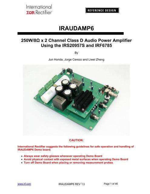
<strong>IRAUDAMP6</strong><br />
250W/8Ω x 2 Channel Class D Audio Power Amplifier<br />
Using the IRS20957S and IRF6785<br />
By<br />
Jun Honda, Jorge Cerezo and Liwei Zheng<br />
CAUTION:<br />
<strong>International</strong> <strong>Rectifier</strong> suggests the following guidelines for safe operation and handling of<br />
<strong>IRAUDAMP6</strong> Demo board;<br />
• Always wear safety glasses whenever operating Demo Board<br />
• Avoid physical contact with exposed metal surfaces when operating Demo Board<br />
• Turn off Demo Board when placing or removing measurement probes<br />
www.irf.com Page 1 of 46<br />
<strong>IRAUDAMP6</strong> REV 1.0
TABLE OF CONTENTS<br />
PAGE<br />
INTRODUCTION............................................................................................................................................... 3<br />
SPECIFICATIONS ............................................................................................................................................ 3<br />
CONNECTION SETUP..................................................................................................................................... 5<br />
CONNECTOR DESCRIPTION ......................................................................................................................... 6<br />
TEST PROCEDURES....................................................................................................................................... 6<br />
PERFORMANCE AND TEST GRAPHS .......................................................................................................... 7<br />
<strong>IRAUDAMP6</strong> OVERVIEW .............................................................................................................................. 12<br />
FUNCTIONAL DESCRIPTIONS..................................................................................................................... 13<br />
CLASS D OPERATION..................................................................................................................................... 13<br />
POWER SUPPLIES.......................................................................................................................................... 13<br />
BUS PUMPING ............................................................................................................................................... 14<br />
HOUSE KEEPING POWER SUPPLY................................................................................................................... 14<br />
INPUT............................................................................................................................................................ 15<br />
OUTPUT ........................................................................................................................................................ 15<br />
LOAD IMPEDANCE .......................................................................................................................................... 15<br />
GAIN SETTING / VOLUME CONTROL ................................................................................................................ 16<br />
EFFICIENCY................................................................................................................................................... 16<br />
OUTPUT FILTER DESIGN AND PREAMPLIFIER................................................................................................... 17<br />
SELF-OSCILLATING PWM MODULATOR .......................................................................................................... 17<br />
ADJUSTMENTS OF SELF-OSCILLATING FREQUENCY......................................................................................... 18<br />
SWITCHES AND INDICATORS........................................................................................................................... 18<br />
STARTUP AND SHUTDOWN ............................................................................................................................. 18<br />
CLICK AND POP NOISE REDUCTION ............................................................................................................... 19<br />
STARTUP AND SHUTDOWN SEQUENCING ........................................................................................................ 20<br />
SELECTABLE DEAD-TIME................................................................................................................................ 23<br />
LEVEL SHIFTERS ........................................................................................................................................... 23<br />
PROTECTION SYSTEM OVERVIEW................................................................................................................... 24<br />
Over-Current Protection (OCP)............................................................................................................... 24<br />
Over-Voltage Protection (OVP)............................................................................................................... 26<br />
Under-Voltage Protection (UVP) ............................................................................................................. 26<br />
Speaker DC-Voltage Protection (DCP)................................................................................................... 27<br />
Offset Null (DC Offset) Adjustment ......................................................................................................... 27<br />
Over-Temperature Protection (OTP) ...................................................................................................... 27<br />
Thermal Considerations .......................................................................................................................... 27<br />
Thermal Interface Material’s Pressure Control ....................................................................................... 28<br />
AMP6 Thermal pad pressure control calculation .................................................................................... 30<br />
Short Circuit Protection Response.......................................................................................................... 31<br />
<strong>IRAUDAMP6</strong> FABRICATION MATERIALS................................................................................................... 37<br />
<strong>IRAUDAMP6</strong> PCB SPECIFICATIONS........................................................................................................... 42<br />
REVISION CHANGES DESCRIPTIONS........................................................................................................ 46<br />
www.irf.com Page 2 of 46<br />
<strong>IRAUDAMP6</strong> REV 1.0
Introduction<br />
The <strong>IRAUDAMP6</strong> reference design is a two-channel, 250W/ch (8Ω) load half-bridge Class D audio power<br />
amplifier. This reference design demonstrates how to use the IRS20957S Class D audio controller and gate<br />
driver IC, implement protection circuits, and design an optimum PCB layout using the IRF6785 DirectFET<br />
MOSFETs. This reference design does not require increasing the size of the heatsink or require fan cooling<br />
for normal operation (one-eighth of continuous rated power).The reference design provides all the required<br />
housekeeping power supplies for ease of use. The two-channel design is scalable for power and the number<br />
of channels.<br />
Applications<br />
• AV receivers<br />
• Home theater systems<br />
• Mini component stereos<br />
• Powered speakers<br />
• Sub-woofers<br />
• Musical Instrument amplifiers<br />
Features<br />
Output Power:<br />
Residual Noise:<br />
Distortion:<br />
Efficiency:<br />
Multiple Protection Features:<br />
PWM Modulator:<br />
250W x 2 channels (8Ω load),<br />
90µV, IHF-A weighted, AES-17 filter<br />
0.005% THD+N @ 125W, 8Ω<br />
96% @ 250W, 8Ω, single-channel driven, Class D stage<br />
Over-current protection (OCP), high side and low side<br />
Over-voltage protection (OVP),<br />
Under-voltage protection (UVP), high side and low side<br />
DC-protection (DCP),<br />
Over-temperature protection (OTP)<br />
Self-oscillating half-bridge topology with optional clock synchronization<br />
Specifications<br />
General Test Conditions (unless otherwise noted) Notes / Conditions<br />
Supply Voltages<br />
±73.5V<br />
Load Impedance 8-4Ω<br />
Self-Oscillating Frequency 400kHz No input signal, Adjustable<br />
Gain Setting 33dB 1Vrms input yields rated power<br />
Electrical Data Typical Notes / Conditions<br />
IR Devices Used<br />
IRS20957S Audio Controller and Gate-Driver,<br />
IRF6785 DirectFET MOSFETs<br />
Modulator<br />
Self-oscillating, second order sigma-delta modulation, analog input<br />
Power Supply Range ± 38V to ±75V Bipolar power supply<br />
Output Power CH1-2: (1% THD+N) 320W 1kHz<br />
Output Power CH1-2: (10% THD+N) 410W 1kHz<br />
www.irf.com Page 3 of 46<br />
<strong>IRAUDAMP6</strong> REV 1.0
Rated Load Impedance 8-4Ω Resistive load<br />
Idling Supply Current ±85mA No input signal<br />
Total Idle Power Consumption 11.9W No input signal<br />
Channel Efficiency 96% Single-channel driven,<br />
250W, Class D stage<br />
.<br />
Audio Performance<br />
THD+N, 1W<br />
THD+N, 10W<br />
THD+N, 60W<br />
THD+N, 100W<br />
THD+N, 200W<br />
*Before<br />
Demodula<br />
tor<br />
0.008%<br />
0.003%<br />
0.0015%<br />
0.002%<br />
0.009%<br />
Class D<br />
Output<br />
0.008%<br />
0.004%<br />
0.002%<br />
0.004%<br />
0.009%<br />
Notes / Conditions<br />
1kHz, Single-channel driven<br />
Dynamic Range 117dB 113dB<br />
A-weighted, AES-17 filter,<br />
Single-channel operation<br />
Residual Noise, 22Hz - 20kHzAES17 70µV 110µV Self-oscillating – 400kHz<br />
Damping Factor 2000 906 1kHz, relative to 8Ω load<br />
Channel Separation<br />
92dB<br />
90dB<br />
72dB<br />
92dB<br />
80dB<br />
62dB<br />
100Hz<br />
1kHz<br />
10kHz<br />
Frequency Response : 20Hz-20kHz<br />
: 20Hz-35kHz<br />
N/A<br />
±0.25dB<br />
±1dB<br />
1W, 8Ω Load<br />
Thermal Performance Typical Notes / Conditions<br />
Idling T C =30°C<br />
No signal input, T A =25°C<br />
T PCB =36°C<br />
2ch x 31.25W (1/8 rated power) T C =54°C<br />
Continuous, T A =25°C<br />
T PCB =65°C<br />
2ch x 250W (Rated power) T C =80°C<br />
At OTP shutdown @ 150 sec,<br />
T PCB =106°C<br />
T A =25°C<br />
Physical Specifications<br />
Dimensions<br />
Weight<br />
7.76”(L) x 5.86”(W) x 2.2”(H)<br />
192 mm (L) x 149mm (W) x56mm(H)<br />
0.54kgm<br />
www.irf.com Page 4 of 46<br />
<strong>IRAUDAMP6</strong> REV 1.0
Connection Setup<br />
73.5V,8A DC supply<br />
73.5V,8A DC supply<br />
250W,Non-inductive Resistors<br />
8~4 Ohm<br />
8~4 Ohm<br />
J1<br />
CH1 Output<br />
G<br />
J3<br />
J5<br />
CH2 Output<br />
S3<br />
J8<br />
S2<br />
Normal<br />
J7<br />
J9<br />
J6<br />
Protection<br />
CH1<br />
Input<br />
CH2<br />
Input<br />
Volume<br />
R100<br />
S1<br />
Audio Signal Generator<br />
Fig 1 Typical Test Setup<br />
www.irf.com Page 5 of 46<br />
<strong>IRAUDAMP6</strong> REV 1.0
Connector Description<br />
CH1 IN J7 Analog input for CH1<br />
CH2 IN J9 Analog input for CH2<br />
POWER J3 Positive and negative supply (+B / -B)<br />
CH1 OUT J1 Output for CH1<br />
CH2 OUT J5 Output for CH2<br />
EXT CLK J6 External clock sync<br />
DCP OUT J8 DC protection relay output<br />
Test Procedures<br />
Test Setup:<br />
1. Connect 8Ω-250 W dummy loads to output connectors (J1 and J5 as shown on Fig 1) and<br />
parallel it with input of Audio Precision analyzer (AP).<br />
2. Connect the Audio Signal Generator to J7 and J9 for CH1 and CH2 respectively (AP).<br />
3. Set up the dual power supply with voltages of ±73.5V;set current limit to 8A.<br />
4. TURN OFF the dual power supply before connecting to ON of the unit under test (UUT).<br />
5. Set switch S1 to middle position (self oscillating).<br />
6. Set volume level knob R130 fully counter-clockwise (minimum volume).<br />
7. Connect the dual power supply to J3. as shown on Fig 1<br />
Power up:<br />
8. Turn ON the dual power supply. The ±B supplies must be applied and removed at the<br />
same time.<br />
9. Red LED (Protection) should turn on almost immediately and turn off after about 3s.<br />
10. Green LED (Normal) then turns on after red LED is extinguished and should stay on.<br />
11. Quiescent current for the positive supply should be 84mA ±10mA at +73.5V.<br />
12. Quiescent current for the negative supply should be 80mA ±10mA at –73.5V.<br />
13. Push S3 switch(Trip and Reset push-buttom)to restart the sequence of LEDs<br />
indicators,which should be the same as noted above in steps 9-10.<br />
Switching Frequency test<br />
14. Monitor switching waveform at VS1/J4(pin9-12)of CH1 and VS2/J3(pin1-4)CH2 on<br />
Daughter Board using an Oscilloscope.<br />
15. For <strong>IRAUDAMP6</strong>, the self-oscillating switching frequency is pre-calibrated to 400 KHz. To<br />
modify the <strong>IRAUDAMP6</strong> frequency, change the values of potentiometers R49 and R74 for<br />
CH1 and CH2 respectively.<br />
www.irf.com Page 6 of 46<br />
<strong>IRAUDAMP6</strong> REV 1.0
Functionality Audio Tests:<br />
16. Apply 1V RMS at 1kHz sinusoidal signal from the Audio Signal Generator.<br />
17. Turn control volume up (R130 clock-wise) to obtain an output reading of 250Watts.<br />
18. For all subsequent tests as shown on the Audio Precision graphs below (Fig 2- Fig7), the<br />
measurements are taken across J1 and J5 with an AES-17 Filter. Observe that a 1 V RMS<br />
input generates an output voltage of 44.7 V RMS .<br />
19. Sweep the audio signal voltage from 15 mV RMS to 1 V RMS .<br />
20. Monitor the output signals at J1/J5 with an oscilloscope. The waveform must be a non<br />
distorted sinusoidal signal.<br />
Test Setup using Audio Precision (Ap):<br />
21. Use an unbalanced-floating signal from the generator outputs.<br />
22. Use balanced inputs taken across output terminals, J1 and J5.<br />
23. Connect Ap frame ground to GND at terminal J7/J9.<br />
24. Select the AES-17 filter(pull-down menu) for all the testing except frequency response.<br />
25. Sweep the input signal voltage from 15 mV RMS to 1 V RMS .<br />
26. Run Ap test programs for all subsequent tests as shown in Fig 2- Fig 7below.<br />
Performance and test graphs<br />
1 0<br />
5<br />
2<br />
1<br />
0 . 5<br />
0 . 2<br />
%<br />
0 . 1<br />
0 . 0 5<br />
0 . 0 2<br />
0 . 0 1<br />
0 . 0 0 5<br />
0 . 0 0 2<br />
0 . 0 0 1<br />
1 0 0 m 2 0 0 m 5 0 0 m 1 2 5 1 0 2 0 5 0 1 0 0 2 0 0 5 0 0 1 k<br />
W<br />
S w e e p T ra c e C o lo r L in e S t y le T h ic k D a t a A x is C o m m e n t<br />
1 1 B lu e S o lid 2 A n lr. T H D + N R a t io L e ft C H 2<br />
1 3 R e d S o lid 2 A n lr. T H D + N R a t io L e ft C H 1<br />
±B Supply = ±73.5V, 8 Ω Resistive Load<br />
Fig 2 <strong>IRAUDAMP6</strong>, THD+N versus Power, Stereo, 8 Ω<br />
www.irf.com Page 7 of 46<br />
<strong>IRAUDAMP6</strong> REV 1.0
8 ohm load<br />
4 ohm load<br />
Fig 3 <strong>IRAUDAMP6</strong>, Frequency response<br />
www.irf.com Page 8 of 46<br />
<strong>IRAUDAMP6</strong> REV 1.0
100<br />
.<br />
10<br />
1<br />
%<br />
0.1<br />
0.01<br />
0.001<br />
0.0001<br />
20 50 100 200 500 1k 2k 5k 10k 20k<br />
Hz<br />
Sweep Trace Color Line Style Thick Data Axis Comment<br />
1 1 Red Solid 2 Anlr.THD+N Ratio Left 125W L<br />
1 2 Blue Solid 2 Anlr.THD+N Ratio Left 125W R<br />
2 1 Magenta Solid 2 Anlr.THD+N Ratio Left 25W L<br />
2 2 Green Solid 1 Anlr.THD+N Ratio Left 25W R<br />
Fig 4 THD+N Ratio vs. Frequency<br />
www.irf.com Page 9 of 46<br />
<strong>IRAUDAMP6</strong> REV 1.0
+0<br />
-20<br />
d<br />
B<br />
V<br />
-40<br />
-60<br />
-80<br />
-100<br />
10 20 50 100 200 500 1k 2k 5k 10k 20k<br />
Hz<br />
Sweep Trace Color Line Style Thick Data Axis Comment<br />
1 1 Magenta Solid 1 Fft.Ch.1 Ampl Left<br />
1 2 Blue Solid 1 Fft.Ch.2 Ampl Left<br />
Fig 5, 1V output Frequency Spectrum<br />
+20<br />
+0<br />
-20<br />
d<br />
B<br />
V<br />
-40<br />
-60<br />
-80<br />
-100<br />
-120<br />
-140<br />
10 20 50 100 200 500 1k 2k 5k 10k 20k<br />
Hz<br />
Sweep Trace Color Line Style Thick Data Axis Comment<br />
1 1 Red Solid 1 Fft.Ch.1 Ampl Left<br />
1 2 Blue Solid 1 Fft.Ch.2 Ampl Left<br />
No signal, Self Oscillator @ 400kHz<br />
Fig 6, <strong>IRAUDAMP6</strong> Noise Floor<br />
www.irf.com Page 10 of 46<br />
<strong>IRAUDAMP6</strong> REV 1.0
.<br />
Fig 7, Channel separation vs. frequency<br />
.<br />
www.irf.com Page 11 of 46<br />
<strong>IRAUDAMP6</strong> REV 1.0
<strong>IRAUDAMP6</strong> Overview<br />
The <strong>IRAUDAMP6</strong> features a 2CH self-oscillating type PWM modulator for the lowest component<br />
count, highest performance and robust design. This topology represents an analog version of a<br />
second-order sigma-delta modulation having a Class D switching stage inside the loop. The<br />
benefit of the sigma-delta modulation, in comparison to the carrier-signal based modulation, is that<br />
all the error in the audible frequency range is shifted to the inaudible upper-frequency range by<br />
nature of its operation. Also, sigma-delta modulation allows a designer to apply a sufficient<br />
amount of error correction.<br />
The <strong>IRAUDAMP6</strong> self-oscillating topology consists of following essential functional blocks.<br />
• Front-end integrator<br />
• PWM comparator<br />
• Level shifters<br />
• Gate drivers and MOSFETs<br />
• Output LPF<br />
Feedback<br />
Σ<br />
U1<br />
Integrator<br />
Daughter-board<br />
U1<br />
+B<br />
LPF<br />
GND<br />
IRS20957S<br />
Gate Driver<br />
IRF6785<br />
Direct-FET<br />
-B<br />
Fig 8, Simplified Block Diagram of Class D Amplifier<br />
www.irf.com Page 12 of 46<br />
<strong>IRAUDAMP6</strong> REV 1.0
Functional Descriptions<br />
Class D Operation<br />
Referring to CH1 as an example, the op-amp U6 forms a front-end second-order integrator with<br />
C38, C42 & R50 + R49P. This integrator receives a rectangular feedback waveform from the<br />
Class D switching stage and outputs a quadratic oscillatory waveform as a carrier signal. To<br />
create the modulated PWM signal, the input signal shifts the average value of this quadratic<br />
waveform (through gain relationship between R40,AR154 and R38 + R39) so that the duty varies<br />
according to the instantaneous value of the analog input signal. The IRS20957 input comparator<br />
processes the signal to create the required PWM signal. This PWM signal is internally level-shifted<br />
down to the negative supply rail where this signal is split into two signals, with opposite polarity<br />
and added deadtime, for high-side and low-side MOSFET gate signals, respectively. The<br />
IRS20957 drives two IRF6785 DirectFET MOSFETs in the power stage to provide the amplified<br />
PWM waveform. The amplified analog output is re-created by demodulating the amplified PWM.<br />
This is done by means of the LC low-pass filter (LPF) formed by L4 and C34, which filters out the<br />
Class D switching carrier signal.<br />
Power Supplies<br />
The <strong>IRAUDAMP6</strong> has all the necessary housekeeping power supplies onboard and only requires<br />
a pair of symmetric power supplies ranging from ±38 V to ±82 V (+B, GND, -B) for operation. The<br />
internally-generated housekeeping power supplies include a ±5 V supply for analog signal<br />
processing (preamp, etc.), while a +12 V supply (V CC ), referenced to –B, is included to supply the<br />
Class D gate-driver stage.<br />
For the externally-applied power, a regulated power supply is preferable for performance<br />
measurements, but not always necessary. The bus capacitors, C45 ~ C48 on the motherboard,<br />
along with high-frequency bypass-caps C19 ~ C26 on daughter board, address the high-frequency<br />
ripple current that result from switching action. In designs involving unregulated power supplies,<br />
the designer should place a set of bus capacitors, having enough capacitance to handle the audioripple<br />
current, externally. Overall regulation and output voltage ripple for the power supply design<br />
are not critical when using the <strong>IRAUDAMP6</strong> Class D amplifier as the power supply rejection ratio<br />
(PSRR) of the <strong>IRAUDAMP6</strong> is excellent (Fig 9).<br />
www.irf.com Page 13 of 46<br />
<strong>IRAUDAMP6</strong> REV 1.0
Fig 9, Amp6 Power Supply Rejection Ratio (PSRR)<br />
Bus Pumping<br />
Since the <strong>IRAUDAMP6</strong> is a half-bridge configuration, bus pumping does occur. Under normal<br />
operation during the first half of the cycle, energy flows from one supply through the load and into<br />
the other supply, thus causing a voltage imbalance by pumping up the bus voltage of the receiving<br />
power supply. In the second half of the cycle, this condition is opposite, resulting in bus pumping<br />
of the other supply.<br />
These conditions worsen bus pumping:<br />
– Lower frequencies (bus-pumping duration is longer per half cycle)<br />
– Higher power output voltage and/or lower load impedance (more energy transfers between<br />
supplies)<br />
– Smaller bus capacitors (the same energy will cause a larger voltage increase)<br />
The <strong>IRAUDAMP6</strong> has protection features that will shutdown the switching operation if the bus<br />
voltage becomes too high (>82 V) or too low (
Input<br />
A proper input signal is an analog signal ranging from 20Hz to 20kHz with up to 3 V RMS amplitude<br />
with a source impedance of no more than 600 Ω. Input signal with frequencies from 30kHz to<br />
60kHz may cause LC resonance in the output LPF, causing a large reactive current flowing<br />
through the switching stage, and the LC resonance can activate OCP.<br />
The <strong>IRAUDAMP6</strong> has an RC network called a Zobel network (R45 and C36) to damp the<br />
resonance and prevent peaking frequency response with light loading impedance. (Fig 10), but is<br />
not thermally rated to handle continuous supersonic frequencies. These supersonic input<br />
frequencies therefore should be avoided. Separate mono RCA connectors provide input to each of<br />
the two channels. Although both channels share a common ground, it is necessary to connect<br />
each channel separately to limit noise and crosstalk between channels.<br />
Fig 10 Output Low Pass Filter and Zobel Network<br />
Output<br />
Both outputs for the <strong>IRAUDAMP6</strong> are single-ended and therefore have terminals labeled (+) and (-<br />
) with the (-) terminal connected to power ground. Each channel is optimized for a 8 Ω speaker<br />
load for a maximum output power of 250 W.<br />
Load Impedance<br />
Each channel is optimized for a 8 Ω speaker load in half bridge.<br />
www.irf.com Page 15 of 46<br />
<strong>IRAUDAMP6</strong> REV 1.0
Gain Setting / Volume Control<br />
The <strong>IRAUDAMP6</strong> has an internal volume control (potentiometer R130 labeled, “VOLUME”) for<br />
gain adjustment. Gain settings for both channels are tracked and controlled by the volume control<br />
IC (U_2) setting the gain from the microcontroller IC (U_3). The total gain is a product of the<br />
power-stage gain, which is constant (+33 dB), and the input-stage gain that is directly-controlled<br />
by the volume adjustment. The volume range is about 100 dB with minimum volume setting to<br />
mute the system with an overall gain of less than -60 dB. For best performance in testing, the<br />
internal volume control should be set to 1 Vrms input will result in rated output power (250 W into<br />
8 Ω).<br />
Efficiency<br />
Fig 11 shows efficiency characteristics of the <strong>IRAUDAMP6</strong>. The high efficiency is achieved by<br />
following major factors:<br />
1) Low conduction loss due to the DirectFETs offering low R DS(ON)<br />
2) Low switching loss due to the DirectFETs offering low input capacitance for fast rise and<br />
fall times<br />
Secure dead-time provided by the IRS20957, avoiding cross-conduction<br />
100%<br />
90%<br />
80%<br />
Efficiency (%)<br />
70%<br />
60%<br />
50%<br />
40%<br />
30%<br />
Class D Efficiency<br />
20%<br />
10%<br />
0%<br />
0 50 100 150 200 250 300 350 400<br />
Output Power(W)<br />
Fig 11, <strong>IRAUDAMP6</strong> 8 ohms load Stereo, ±B supply = ±73.5V<br />
www.irf.com Page 16 of 46<br />
<strong>IRAUDAMP6</strong> REV 1.0
Output Filter Design and Preamplifier<br />
The audio performance of the <strong>IRAUDAMP6</strong> depends on a number of different factors. The section<br />
entitled, “Typical Performance” presents performance measurements based on the overall system,<br />
including the preamp and output filter. While the preamp and output filter are not part of the Class<br />
D power stage, they have a significant effect on the overall performance.<br />
Output filter<br />
The amplified PWM output is reconstructed back to an analog signal by the output LC LPF.<br />
Demodulation LC low-pass filter (LPF) formed by L4 and C34, filters out the Class D switching<br />
carrier signal leaving the audio output at the speaker load. A single stage output filter can be used<br />
with switching frequencies of 400 kHz and greater; a design with a lower switching frequency may<br />
require an additional stage of LPF.<br />
Since the output filter is not included in the control loop of the <strong>IRAUDAMP6</strong>, the reference design<br />
cannot compensate for performance deterioration due to the output filter. Therefore, it is important<br />
to understand what characteristics are preferable when designing the output filter:<br />
1) The DC resistance of the inductor should be minimal and be within 20 m_Ohm or less.<br />
2) The linearity of the output inductor and capacitor should be high with respect to load<br />
current and voltage.<br />
Preamplifier<br />
The preamp allows partial gain of the input signal, and in the <strong>IRAUDAMP6</strong>, controls the volume.<br />
The preamp itself will add distortion and noise to the input signal, resulting in a gain through the<br />
Class D output stage and appearing at the output. Even a few micro-volts of noise can add<br />
significantly to the output noise of the overall amplifier. In fact, the output noise from the preamp<br />
contributes more than half of the overall noise to the system.<br />
It is possible to evaluate the performance without the preamp and volume control, by moving<br />
resistors R154and R155 to R157 and R156, respectively. This effectively bypasses the preamp<br />
and connects the RCA inputs directly to the Class D power stage input. Improving the selection of<br />
preamp and/or output filter, will improve the overall system performance to approach that of the<br />
stand-alone Class D power stage.<br />
Self-Oscillating PWM Modulator<br />
The <strong>IRAUDAMP6</strong> Class D audio power amplifier features a self-oscillating type PWM modulator<br />
for the lowest component count and robust design. This topology represents an analog version of<br />
a second-order sigma-delta modulation having a Class D switching stage inside the loop. The<br />
benefit of the sigma-delta modulation, in comparison to the carrier-signal based modulation, is that<br />
all the error in the audible frequency range is shifted to the inaudible upper-frequency range by<br />
nature of its operation. Also, sigma-delta modulation allows a designer to apply a sufficient<br />
amount of correction.<br />
The self-oscillating frequency is determined by the total delay time inside the control loop of the<br />
system. The delay of the logic circuits, the IRS20957 gate-driver propagation delay, the IRF6785<br />
switching speed, the time-constant of front-end integrator (e.g. R50 + R49, C38 and C42 for CH1)<br />
www.irf.com Page 17 of 46<br />
<strong>IRAUDAMP6</strong> REV 1.0
and variations in the supply voltages are critical factors of the self-oscillating frequency. Under<br />
normal conditions, the switching-frequency is around 400 kHz with no audio input signal and a +/-<br />
73.5 V supply.<br />
Adjustments of Self-Oscillating Frequency<br />
The PWM switching frequency in this type of self-oscillating switching scheme greatly impacts the<br />
audio performance, both in absolute frequency and frequency relative to the other channels. In<br />
absolute terms, at higher frequencies, distortion due to switching-time becomes significant, while<br />
at lower frequencies, the bandwidth of the amplifier suffers. In relative terms, interference between<br />
channels is most significant if the relative frequency difference is within the audible range.<br />
Normally when adjusting the self-oscillating frequency of the different channels, it is best to either<br />
match the frequencies accurately, or have them separated by at least 25 kHz.<br />
Potentiometers for adjusting self-oscillating frequency<br />
R49<br />
Switching frequency for CH1*<br />
R74<br />
Switching frequency for CH2*<br />
*Adjustments have to be done at an idling condition with no signal input.<br />
Switches and Indicators<br />
There are two different indicators on the reference design:<br />
– A Red LED, signifying a fault / shutdown condition when lit.<br />
– A green LED on the motherboard, signifying conditions are normal and no fault condition is<br />
present.<br />
There are three switches on the reference design:<br />
– Switch S1 is an oscillator selector. This three-position switch is selectable for internal selfoscillator<br />
(middle position – “SELF”), or either internal (“INT”) or external (“EXT”) clock<br />
synchronization.<br />
– Switch S2 is an internal clock-sync phase difference selector. This feature allows the designer<br />
to modify the clock-sync phase separation in order to avoid synchronized switching noise<br />
interference. With S2 is set to OFF, the sync-clock phase difference value is 180°.With S2 is<br />
set to INT, the clock-sync phase is set by potentiometer R100. With S2 is set to STG, one<br />
channel’s clock is quadrature-lagging<br />
– Switch S3 is a trip and reset push-button. Pushing this button has the same effect of a fault<br />
condition. The circuit will restart about three seconds after the shutdown button is released.<br />
Startup and Shutdown<br />
One of the most important aspects of any audio amplifier is the startup and shutdown procedures.<br />
Typically, transients occurring during these intervals can result in audible pop- or click-noise on the<br />
output speaker. Traditionally, these transients have been kept away from the speaker through the<br />
use of a series relay that connects the speaker to the audio amplifier only after the startup<br />
transients have passed and disconnects the speaker prior to shutting down the amplifier. It is<br />
interesting to note that the audible noise of the relay opening and closing is not considered “click<br />
noise”, although in some cases, it can be louder than the click noise of non-relay-based solutions.<br />
www.irf.com Page 18 of 46<br />
<strong>IRAUDAMP6</strong> REV 1.0
The <strong>IRAUDAMP6</strong> does not use any series relay to disconnect the speaker from the audible<br />
transient noise, but rather a shunt-based click noise reduction circuit that yields audible noise<br />
levels that are far less that those generated by the relays they replace. This results in a more<br />
reliable, superior performance system.<br />
For the startup and shutdown procedures, the activation (and deactivation) of the click-noise<br />
reduction circuit, the Class D power stage and the audio input (mute) controls have to be<br />
sequenced correctly to achieve the required click noise reduction. The overall startup sequencing,<br />
shutdown sequencing and shunt circuit operation are described below.<br />
Click and POP Noise Reduction<br />
To reduce the turn-on and turn-off click noise, a low impedance shunting circuit is used to<br />
minimize the voltage across the speaker during transients. For this purpose, the shunting circuit<br />
must include the following characteristics:<br />
1) An impedance significantly lower than that of the speaker being shunted. In this case, the<br />
shunt impedance is ~100 mΩ, compared to the normal 8 Ω speaker impedance.<br />
2) When deactivated, the shunting circuit must be able to block voltage in both directions due<br />
to the bi-directional nature of the audio output.<br />
3) The shunt circuit requires some form of OCP. If one of the Class D output MOSFETs fails,<br />
or is conducting when the speaker mute (SP MUTE) is activated, the shunting circuit will<br />
effectively try to short one of the two supplies (+/-B).<br />
The implemented click-noise reduction circuit is shown in Figure 12. Before startup or shutdown of<br />
the Class D power stage, the click-noise reduction circuit is activated through the SP MUTE<br />
control signal. With SP MUTE signal high, the speaker output is shorted through the back-to-back<br />
MOSFETs (U5 for Channel 1) with an equivalent on resistance of about 100 mΩ. The two<br />
transistors (U7 for Channel 1) are for the OCP circuit.<br />
+B<br />
Speaker Mute<br />
Click noise<br />
reduction circuit<br />
-B<br />
Transient<br />
current paths<br />
Over Current<br />
Protection<br />
Fig 12, Class D Output Stage with Click-Noise Reduction Circuit<br />
www.irf.com Page 19 of 46<br />
<strong>IRAUDAMP6</strong> REV 1.0
Startup and Shutdown Sequencing<br />
The <strong>IRAUDAMP6</strong> sequencing is achieved through the charging and discharging of the CStart<br />
capacitor C66. This, coupled to the charging and discharging of the voltage of CSD (C11 on<br />
daughter board for CH1) of the IRS20957, is all that is required for complete sequencing. The<br />
conceptual startup and shutdown timing diagrams are show in Figure 13.<br />
CStart Ref1<br />
CStart Ref2<br />
+B<br />
+5 V<br />
-5 V<br />
CSD= 2/3V DD<br />
CSD<br />
CStart<br />
Time<br />
UVP@-20 V<br />
V CC<br />
-B<br />
CHx_O<br />
SP MUTE<br />
Audio MUTE<br />
Class D startup<br />
Music startup<br />
Fig 13, Conceptual Startup Sequencing of Power Supplies and Audio Section Timing<br />
www.irf.com Page 20 of 46<br />
<strong>IRAUDAMP6</strong> REV 1.0
For startup sequencing, +/-B supplies startup at different intervals. As +/-B supplies reach +5 V<br />
and -5 V respectively, the analog supplies (+/-5 V) start charging and, once +B reaches ~16 V, V CC<br />
charges. Once –B reaches -20 V, the UVP is released and CSD and CStart start charging. Once<br />
+/-5 V is established, the click-noise reduction circuit is activated through the SP MUTE control<br />
signal. As CSD reaches two-thirds V DD , the Class D stage starts oscillating. Once the startup<br />
transient has passed, SP MUTE is released (CStart reaches Ref1). The Class D amplifier is now<br />
operational, but the preamp output remains muted until CStart reaches Ref2. At this point, normal<br />
operation begins. The entire process takes less than three seconds.<br />
+B<br />
CStart Ref2<br />
CStart Ref1<br />
CSD= 2/3V DD<br />
CSD<br />
CStart<br />
+5 V<br />
-5 V<br />
Time<br />
V CC<br />
-B<br />
UVP@-20 V<br />
CHx_O<br />
SP MUTE<br />
Music shutdown<br />
Class D shutdown<br />
Audio MUTE<br />
Fig 14, Conceptual Shutdown Sequencing of Power Supplies and Audio Section Timing<br />
Shutdown sequencing is initiated once UVP is activated. As long as the supplies do not discharge<br />
too quickly, the shutdown sequence can be completed before the IRS20957 trips UVP. Once UVP<br />
is activated, CSD and CStart are discharged at different rates. In this case, threshold Ref2 is<br />
reached first and the preamp audio output is muted. Once CStart reaches threshold Ref1, the<br />
click-noise reduction circuit is activated (SP MUTE). It is then possible to shutdown the Class D<br />
stage (CSD reaches two-thirds V DD ). This process takes less than 200 ms.<br />
www.irf.com Page 21 of 46<br />
<strong>IRAUDAMP6</strong> REV 1.0
For any external fault condition (OTP, OVP, UVP or DCP – see “Protection”) that does not lead to<br />
power supply shutdown, the system will trip in a similar manner as described above. Once the<br />
fault is cleared, the system will reset (similar sequence as startup).<br />
CStart Ref2<br />
CStart Ref1<br />
CStart Ref1<br />
CStart Ref2<br />
CSD= 2/3VDD<br />
CSD<br />
CStart<br />
External trip<br />
Reset<br />
Time<br />
CHx_O<br />
SP MUTE<br />
Audio MUTE<br />
Class D shutdown Class D startup<br />
Music shutdown<br />
Music startup<br />
Fig 15, Conceptual Click Noise Reduction Sequencing at Trip and Reset<br />
www.irf.com Page 22 of 46<br />
<strong>IRAUDAMP6</strong> REV 1.0
Selectable Dead-time<br />
The IRS20957 determines its dead-time based on the voltage applied to the DT pin. An internal<br />
comparator translates which pre-determined dead-time is being used by comparing the DT voltage<br />
with internal reference voltages. A resistive voltage divider from V CC sets threshold voltages for<br />
each setting, negating the need for a precise absolute voltage to set the mode. The threshold<br />
voltages between dead-time settings are set internally, based on different ratios of V CC as<br />
indicated in the diagram below. In order to avoid drift from the input bias current of the DT pin, a<br />
bias current of greater than 0.5 mA is suggested for the external resistor divider circuit. Suggested<br />
values of resistance that are used to set a dead-time are given below. Resistors with up to 5%<br />
tolerance can be used.<br />
Dead-time mode Dead-time R22 R19 DT Voltage<br />
DT1 ~15 ns
Protection System Overview<br />
The IRS20957 integrates over current protection (OCP) inside the IC. The rest of the protections,<br />
such as over-voltage protection (OVP), under-voltage protection (UVP), and over temperature<br />
protection (OTP), are detected externally to the IRS20957.<br />
Fig 18, Functional Block Diagram of Protection Circuit Implementation<br />
The external shutdown circuit will disable the output by pulling down CSD pins . If the fault<br />
condition persists, the protection circuit stays in shutdown until the fault is removed.<br />
.<br />
Over-Current Protection (OCP)<br />
The OCP internal to the IRS20957 shuts down the IC if an OCP is sensed in either of the output<br />
MOSFETs. For a complete description of the OCP circuitry, please refer to the IRS20957<br />
datasheet. Here is a brief description:<br />
www.irf.com Page 24 of 46<br />
<strong>IRAUDAMP6</strong> REV 1.0
Low-Side Current Sensing<br />
The low-side current sensing feature protects the low side DirectFET from an overload condition<br />
from negative load current by measuring drain-to-source voltage across R DS(ON) during its on state.<br />
OCP shuts down the switching operation if the drain-to-source voltage exceeds a preset trip level.<br />
The voltage setting on the OCSET pin programs the threshold for low-side over-current sensing.<br />
When the VS voltage becomes higher than the OCSET voltage during low-side conduction, the<br />
IRS20957 turns the outputs off and pulls CSD down to -VSS.<br />
Fig 19 Simplified Functional Block Diagram of Low-Side Current Sensing<br />
High-Side Current Sensing<br />
The high-side current sensing protects the high side DirectFET from an overload condition from<br />
positive load current by measuring drain-to-source voltage across R DS(ON) during its on state. OCP<br />
shuts down the switching operation if the drain-to-source voltage exceeds a preset trip level.<br />
High-side over-current sensing monitors drain-to-source voltage of the high-side DirectFET during<br />
the on state through the CSH and VS pins. The CSH pin detects the drain voltage with reference<br />
to the VS pin, which is the source of the high-side DirectFET. In contrast to the low-side current<br />
sensing, the threshold of the CSH pin to trigger OC protection is internally fixed at 1.2V. An<br />
external resistive divider R30, R32 and R34 are used to program a threshold . An external reverse<br />
blocking diode D8 is required to block high voltage feeding into the CSH pin during low-side<br />
conduction. By subtracting a forward voltage drop of 0.6V at D8, the minimum threshold which can<br />
be set for the high-side is 0.6V across the drain-to-source.<br />
www.irf.com Page 25 of 46<br />
<strong>IRAUDAMP6</strong> REV 1.0
IRS20957S<br />
Fig 20, Simplified Functional Block Diagram of High-Side Current Sensing<br />
Over-Voltage Protection (OVP)<br />
OVP is provided externally to the IRS20957. OVP shuts down the amplifier if the bus voltage<br />
between GND and -B exceeds 82V. The threshold is determined by a Zener diode Z9. OVP<br />
protects the board from harmful excessive supply voltages, such as due to bus pumping at very<br />
low frequency-continuous output in stereo mode.<br />
Under-Voltage Protection (UVP)<br />
UVP is provided externally to the IRS20957. UVP prevents unwanted audible noise output from<br />
unstable PWM operation during power up and down. UVP shuts down the amplifier if the bus<br />
voltage between GND and -B falls below a voltage set by Zener diode Z8.<br />
www.irf.com Page 26 of 46<br />
<strong>IRAUDAMP6</strong> REV 1.0
Speaker DC-Voltage Protection (DCP)<br />
DCP protects speakers against DC output current feeding to its voice coil. DC offset detection<br />
detects abnormal DC offset and shuts down PWM. If this abnormal condition is caused by a<br />
MOSFET failure because one of the high-side or low-side MOSFETs short circuited and remained<br />
in the on state, the power supply needs to be cut off in order to protect the speakers. Output DC<br />
offset greater than ±2.1V triggers DCP.<br />
Offset Null (DC Offset) Adjustment<br />
The <strong>IRAUDAMP6</strong> is designed such that no output-offset nullification is required. DC offsets are<br />
tested to be less than ±5 mV.<br />
.<br />
Over-Temperature Protection (OTP)<br />
A separate PTC resistor is placed in close proximity to the high-side IRF6785 DirectFET MOSFET<br />
for each of the amplifier channels. If the resistor temperature rises above 90 °C, the OTP is<br />
activated. The OTP protection will only shutdown the relevant channel by pulling low the CSD pin<br />
and will recover once the temperature at the PTC has dropped sufficiently. This temperature<br />
protection limit yields a PCB temperature at the MOSFET of about 100 °C. This setting is limited<br />
by the PCB material and not by the operating range of the MOSFET.<br />
Thermal Considerations<br />
With this high efficiency, the <strong>IRAUDAMP6</strong> design can handle one-eighth of the continuous rated<br />
power, which is generally considered to be a normal operating condition for safety standards.<br />
Without increasing the size of a heatsink or forced air-cooling, the daughter board cannot handle<br />
continuous rated power.<br />
www.irf.com Page 27 of 46<br />
<strong>IRAUDAMP6</strong> REV 1.0
Thermal Interface Material’s Pressure Control<br />
The DirectFET MOSFETs are attached to a heatsink with a thermal interface material (TIM). The<br />
pressure between DirectFET and TIM is controlled by depth of Heat Spreader’s groove. Choose<br />
TIM which is recommended by IR. (Refer to AN-1035 for more details). TIM’s manufacturer<br />
thickness, conductivity, & etc. determine pressure requirement. Below shows selection options<br />
recommended:<br />
Fig 21, TIM Information<br />
www.irf.com Page 28 of 46<br />
<strong>IRAUDAMP6</strong> REV 1.0
Check the TIM’s compression deflection with constant rate of strain (example as Fig.10) base on<br />
manufacturer’s datasheet. According to the stress requirement, find strain range for the TIM. Then,<br />
calculate heat spreader groove depth as below:<br />
Groove Depth=DirectFET’s Height +TIM’s Thickness*strain<br />
**DirectFET’s height should be measured from PCB to the top of DirectFET after reflow. The<br />
average height of IRF6785 is 0.65mm.<br />
Fig 22, compression deflection with constant rate of strain<br />
www.irf.com Page 29 of 46<br />
<strong>IRAUDAMP6</strong> REV 1.0
AMP6 Thermal pad pressure control calculation<br />
PCB thickness=1.6mm<br />
Heatsink thickness=2.54mm Weight=27.1g<br />
(DCC58375837L-18B http://www.alphanovatech.com/c_dcc5837ue.html)<br />
Thermal Pad thickness=2.03mm<br />
(BER164-ND<br />
http://search.digikey.com/scripts/DkSearch/dksus.dll?lang=en&site=US&WT.z_homepage_link=hp_go_butto<br />
n&KeyWords=BER164-ND+)<br />
Spring : S001YJ1D FL=6.4mm SL=2.9mm (http://www.alphanovatech.com/c_springe.html)<br />
Pressure Required:10-50psi(Fig21)<br />
Clearance between push pin and heatsink:<br />
1, Without Spring:<br />
Pin height-PCB thickness-heatsink height(substructure height)-thermal pad thickness<br />
=8.5-1.6-2.54-2.03=2.33mm<br />
2, With Spring:( Assumption: pressure=50pci strain=30% according to Fig22)<br />
Pin height-PCB thickness-heatsink height(substructure height)-thermal pad thickness*70%<br />
=8.5-1.6-2.54-1.421=2.939mm=expected length<br />
Spring length change=Free length-expected length=6.4-2.939=3.461mm<br />
Spring strength= Spring length change*spring rate=3.461*5.19=17.96N<br />
Strength to PCB=4* Spring strength+(heatsink weight*0.00098)=4*17.96+27.1*0.00098=71.87N<br />
To have 50psi pressure we need strength as below:<br />
1kg/cm^2=14.21psi; 1g/cm^2=0.0098N/cm^2<br />
=>50psi=3.51kg/cm^2=3.51*1000*0.0098nN/cm^2=34.398N/cm^2<br />
Heatsink S=5.79*3.68cm^2=21.31cm^2<br />
Total strength we need=34.398*21.31N=732.93N>>71.87N<br />
=>So spring does not have enough strength support push pin more than solid height.<br />
Then, spring height=solid height<br />
Clearance between push pin and heatsink=2.9mm<br />
Pin height-PCB thickness-heatsink height (substructure height)-thermal pad thickness*X%<br />
X=72%<br />
According to Fig22<br />
When Strain=28%, Stress=45psi within the required range 10-50psi<br />
www.irf.com Page 30 of 46<br />
<strong>IRAUDAMP6</strong> REV 1.0
Short Circuit Protection Response<br />
Figs 23-24 show over current protection reaction time of the <strong>IRAUDAMP6</strong> in a short circuit event.<br />
As soon as the IRS20957 detects an over current condition, it shuts down PWM. After one<br />
second, the IRS20957 tries to resume the PWM. If the short circuit persists, the IRS20957 repeats<br />
try and fail sequences until the short circuit is removed.<br />
Short Circuit in Positive and Negative Load Current<br />
CSD pin<br />
CSD pin<br />
VS pin<br />
VS pin<br />
Load current<br />
Load current<br />
Positive OCP<br />
Negative OCP<br />
Fig 23, Positive and Negative OCP Waveforms<br />
.<br />
OCP Waveforms Showing CSD Trip and Hiccup<br />
VS pin<br />
CSD pin<br />
VS pin<br />
CSD pin<br />
Load current<br />
Load current<br />
Fig 24 OCP Response with Continuous Short Circuit<br />
www.irf.com Page 31 of 46<br />
<strong>IRAUDAMP6</strong> REV 1.0
Schematic<br />
www.irf.com <strong>IRAUDAMP6</strong> REV 1.0<br />
Page 32 of 46
www.irf.com <strong>IRAUDAMP6</strong> REV 1.0<br />
Page 33 of 46
www.irf.com <strong>IRAUDAMP6</strong> REV 1.0<br />
Page 34 of 46
www.irf.com <strong>IRAUDAMP6</strong> REV 1.0<br />
Page 35 of 46
Fig 22 <strong>IRAUDAMP6</strong> Schematic<br />
www.irf.com <strong>IRAUDAMP6</strong> REV 1.0<br />
Page 36 of 46
<strong>IRAUDAMP6</strong> Fabrication Materials<br />
Table 1 <strong>IRAUDAMP6</strong> Mother board’s Materials<br />
No P/N Designator Description Quantity Vendor<br />
1 565-1106-ND C1, C33, C50, C75, C77<br />
CAP 10UF 50V ELECT SMG<br />
RAD 5 Digikey<br />
2 PCC13491CT-ND C2, C82, C83<br />
CAP 10UF 16V CERAMIC X7R<br />
1206 3 Digikey<br />
3 565-1147-ND C3, C6, C23, C84, C85, C86<br />
CAP 4.7UF 100V ELECT SMG<br />
RAD 6 Digikey<br />
4 490-1857-1-ND C4, C7, C24<br />
CAP CER 1.0UF 100V 10% X7R<br />
1210 3 Digikey<br />
5 490-1644-1-ND C9, C11, C25<br />
CAP CER 22000PF 50V 5% C0G<br />
0805 3 Digikey<br />
6 478-1403-1-ND C10, C13, C26<br />
CAP CERM .47UF 10% 16V X7R<br />
0805 3 Digikey<br />
7 490-1864-1-ND C12, C16, C27<br />
CAP CER 4.7UF 50V 10% X7R<br />
1210 3 Digikey<br />
8 445-2685-1-ND C14, C19, C28<br />
CAP CER 8200PF 50V C0G 5%<br />
0805 3 Digikey<br />
9 PCC1982CT-ND C15, C20, C29<br />
CAP 330PF 100V CERAMIC<br />
X7R 0805 3 Digikey<br />
10 478-3772-1-ND C17, C21, C30<br />
CAP CERM 6800PF 5% 50V<br />
X7R 0805 3 Digikey<br />
11 478-3746-1-ND C18, C22, C31<br />
CAP CERM 2200PF 5% 100V<br />
X7R 0805 3 Digikey<br />
12 445-2378-1-ND C32, C49<br />
CAP CER 150PF 3000V C0G<br />
10% 1812 2 Digikey<br />
13 338-1178-ND C34, C51<br />
CAP .33UF 2000VDC POLY<br />
FILM AXL 2 Digikey<br />
14 PCE3101CT-ND C35, C64, C65, C69, C79 CAP 10UF 16V ELECT FC SMD 5 Digikey<br />
15 495-1311-ND C36, C53<br />
CAP .10UF 400V METAL<br />
POLYPRO 2 Digikey<br />
16 PCC2009CT-ND C38, C42, C56, C60<br />
CAP CERAMIC 1000PF 200V<br />
NP0 1206 4 Digikey<br />
17 PCC1931CT-ND C39, C57<br />
CAP 2.2UF 16V CERAMIC X7R<br />
1206 2 Digikey<br />
18 478-1281-1-ND C40, C58<br />
CAP CERM 33PF 5% 100V NP0<br />
0805 2 Digikey<br />
19 445-1432-1-ND C41, C43, C59, C61<br />
CAP CER 3.3UF 50V X7R 20%<br />
1210 4 Digikey<br />
20 565-1161-ND C45, C46, C47, C48<br />
CAP 1200UF 100V ELECT SMG<br />
RAD 4 Digikey<br />
21 PCC1812CT-ND C62, C63, C68, C78<br />
CAP .1UF 16V CERAMIC X7R<br />
0805 4 Digikey<br />
22 565-1037-ND C66<br />
CAP 100UF 16V ELECT SMG<br />
RAD 1 Digikey<br />
23 445-1418-1-ND C67<br />
CAP CER .10UF 100V X7R 10%<br />
0805 1 Digikey<br />
24 PCC101CGCT-ND C70<br />
CAP 100PF 50V CERM CHIP<br />
0805 SMD 1 Digikey<br />
25 493-1042-ND C71<br />
CAP 330UF 16V ELECT VR<br />
RADIAL 1 Digikey<br />
26 445-2322-1-ND C72, C73<br />
CAP CER 2200PF 100V C0G 5%<br />
0805 2 Digikey<br />
27 PCC103BNCT-ND C80<br />
CAP 10000PF 50V CERM CHIP<br />
0805 1 Digikey<br />
28 B180DICT-ND D1, D2, D4<br />
DIODE SCHOTTKY 80V 1A<br />
SMA 3 Digikey<br />
29 B1100-FDICT-ND D3<br />
DIODE SCHOTTKY 100V 1A<br />
SMA 1 Digikey<br />
30 641-1166-1-ND D5, D6, D13, D14<br />
DIODE STANDARD 2A 400V<br />
SMB 4 Digikey<br />
31 1N4148WDICT-ND D7, D8, D9, D10, D12, D15, D16, DIODE SWITCH 100V 400MW 8 Digikey<br />
www.irf.com Page 37 of 46<br />
<strong>IRAUDAMP6</strong> REV 1.0
D17<br />
SOD-123<br />
32 1N5819HW-FDICT-ND D11, D18<br />
DIODE SCHOTTKY 40V 1A<br />
SOD123 2 Digikey<br />
33 1N4148WTPMSCT-ND D19, D20, D21, D22<br />
DIODE SWITCH 100V 150MA<br />
SOD123 4 Digikey<br />
34 RS1DB-FDICT-ND D23<br />
DIODE FAST REC 200V 1A<br />
SMB 1 Digikey<br />
35 277-1271-ND J1, J5<br />
CONN TERM BLOCK 2POS<br />
9.52MM PCB 2 Digikey<br />
36 A26453-ND J2<br />
CONN RECEPT 6POS .100<br />
VERT DUAL 1 Digikey<br />
37 277-1272-ND J3<br />
CONN TERM BLOCK 3POS<br />
9.52MM PCB 1 Digikey<br />
38 A26454-ND J4<br />
CONN RECEPT 8POS .100<br />
VERT DUAL 1 Digikey<br />
39 A32248-ND J6<br />
CONN JACK BNC R/A 50 OHM<br />
PCB TIN 1 Digikey<br />
40 CP-1418-ND J7, J9<br />
CONN RCA JACK R/A BLACK<br />
PCB 2 Digikey<br />
41 N/A J8<br />
TERMINAL BLOCK 7.50MM<br />
VERT 2POS 1 Digikey<br />
42 A26453-ND J10<br />
CONN RECEPT 6POS .100<br />
VERT DUAL 1 Digikey<br />
43 513-1051-1-ND L1, L2, L3<br />
INDUCTOR SHIELD PWR<br />
470UH SMD 3 Digikey<br />
44 7G31A-220M-R L4, L5 Class D Inductor,22uH 2 Inductors, Inc<br />
45 160-1143-ND NORMAL1<br />
LED 3MM GREEN<br />
TRANSPARENT 1 Digikey<br />
46 N/A P1<br />
Power MOSFET Photovoltaic<br />
Relay 1 IR<br />
47 160-1140-ND PROTECTION1<br />
LED 3MM HI-EFF RED<br />
TRANSPARENT 1 Digikey<br />
48 FZT855CT-ND Q1, Q3<br />
TRANS NPN 150V 4000MA<br />
SOT-223 2 Digikey<br />
49 MMBTA92DICT-ND Q2<br />
TRANSISTOR PNP -300V SOT-<br />
23 1 Digikey<br />
50 MMBT5401DICT-ND Q7, Q10, Q13<br />
TRANS 150V 350MW PNP SMD<br />
SOT-23 3 Digikey<br />
51 MMBT5551-7DICT-ND Q8, Q9, Q11, Q12, Q14, Q15, Q17<br />
TRANS 160V 350MW NPN SMD<br />
SOT-23 7 Digikey<br />
52 PZT2222ACT-ND Q18<br />
TRANS AMP NPN GP 40V .5A<br />
SOT-223 1 Digikey<br />
53<br />
PZT2907AT1GOSCT-<br />
TRANS SS SW PNP 600MA 60V<br />
ND<br />
Q20<br />
SOT223 1 Digikey<br />
54 PT10XCT-ND R1, R4, R9, R14, R30 RES 10 OHM 1W 5% 2512 SMD 5 Digikey<br />
55 P10KACT-ND R2, R3, R5, R7, R84, R92, R99<br />
RES 10K OHM 1/8W 5% 0805<br />
SMD 7 Digikey<br />
56 P20KACT-ND R6, R142<br />
RES 20K OHM 1/8W 5% 0805<br />
SMD 2 Digikey<br />
57<br />
R56, R79, R82, R88, R101, R107, RES 47 OHM 1/8W 5% 0805<br />
P47ACT-ND<br />
R133, R134, R135<br />
SMD 9 Digikey<br />
58 RHM8.66KCRCT-ND R10<br />
RES 8.66K OHM 1/8W 1% 0805<br />
SMD 1 Digikey<br />
59 P18.7KCCT-ND R11, R17, R32<br />
RES 18.7K OHM 1/8W 1% 0805<br />
SMD 3 Digikey<br />
60 P1.00KCCT-ND R13<br />
RES 1.00K OHM 1/8W 1% 0805<br />
SMD 1 Digikey<br />
61 P4.7KCCT-ND R15, R31<br />
RES 4.70K OHM 1/8W 1% 0805<br />
SMD 2 Digikey<br />
62 P20.5KCCT-ND R16, R19, R37<br />
RES 20.5K OHM 1/8W 1% 0805<br />
SMD 3 Digikey<br />
63 P1.00KCCT-ND R18, R36<br />
R20, R21, R22, R47, R53, R60, R61,<br />
R87, R91, R108, R109, R112, R116,<br />
64 P100KACT-ND<br />
R117, R118, R119, R132, R136<br />
RES 1.00K OHM 1/8W 1% 0805<br />
SMD 2 Digikey<br />
RES 100K OHM 1/8W 5% 0805<br />
SMD 15 Digikey<br />
www.irf.com Page 38 of 46<br />
<strong>IRAUDAMP6</strong> REV 1.0
65<br />
RES 100K OHM METAL FILM<br />
PPC100KW-3JCT-ND R38, R62<br />
3W 5% 2 Digikey<br />
66 P1.0KECT-ND R39, R63<br />
RES 1.0K OHM 1/4W 5% 1206<br />
SMD 2 Digikey<br />
67 P3.3KZCT-ND R40, R64<br />
RES 3.3K OHM 1/10W .1% 0805<br />
SMD 2 Digikey<br />
68 P22KACT-ND R41, R55, R57, R65, R67, R73<br />
RES 22K OHM 1/8W 5% 0805<br />
SMD 6 Digikey<br />
69 P0.0ACT-ND R42, R66<br />
RES 0.0 OHM 1/8W 5% 0805<br />
SMD 2 Digikey<br />
70 PT2.2KXCT-ND R43, R68<br />
RES 2.2K OHM 1W 5% 2512<br />
SMD 2 Digikey<br />
71 PT10XCT-ND R45, R70 RES 10 OHM 1W 5% 2512 SMD 2 Digikey<br />
72 311-470ARCT-ND R46, R71<br />
RES 470 OHM 1/8W 5% 0805<br />
SMD 2 Digikey<br />
73 P4.7ACT-ND R48, R54, R72, R78<br />
RESISTOR 4.7 OHM 1/8W 5%<br />
0805 4 Digikey<br />
74 3361P-102GCT-ND R49, R74<br />
TRIMPOT 1K OHM 6MM SQ<br />
SMD 2 Digikey<br />
75 P100ECT-ND R50, R75, R80, R90, R94<br />
RES 100 OHM 1/4W 5% 1206<br />
SMD 5 Digikey<br />
76<br />
R51, R52, R76, R77, R104, R106, RES 1.0K OHM 1/8W 5% 0805<br />
P1.0KACT-ND<br />
R121, R138<br />
SMD 8 Digikey<br />
77 P200KACT-ND R58, R59<br />
RES 200K OHM 1/8W 5% 0805<br />
SMD 2 Digikey<br />
78 P33KACT-ND R81<br />
RES 33K OHM 1/8W 5% 0805<br />
SMD 1 Digikey<br />
79<br />
R83, R86, R93, R95, R96, R105, RES 47K OHM 1/8W 5% 0805<br />
P47KACT-ND<br />
R111, R123, R129, R139, R140 SMD 11 Digikey<br />
80 P68KACT-ND R85, R97<br />
RES 68K OHM 1/8W 5% 0805<br />
SMD 2 Digikey<br />
81 P4.7KACT-ND R89<br />
RES 4.7K OHM 1/8W 5% 0805<br />
SMD 1 Digikey<br />
82 P100ACT-ND R98, R114, R131<br />
RES 100 OHM 1/8W 5% 0805<br />
SMD 3 Digikey<br />
83 3362H-502LF-ND R100<br />
POT 5.0K OHM 1/4" SQ CERM<br />
SL ST 1 Digikey<br />
84 P330ACT-ND R102<br />
RES 330 OHM 1/8W 5% 0805<br />
SMD 1 Digikey<br />
85 P82KACT-ND R103<br />
RES 82K OHM 1/8W 5% 0805<br />
SMD 1 Digikey<br />
86<br />
R110, R113, R120, R124, R126, RES 5.76K OHM 1/4W 1% 1206<br />
P5.76KFCT-ND<br />
R127<br />
SMD 6 Digikey<br />
87 P10ECT-ND R115<br />
RES 10 OHM 1/4W 5% 1206<br />
SMD 1 Digikey<br />
88 P0.0ECT-ND R122, R128<br />
RES ZERO OHM 1/4W 5% 1206<br />
SMD 2 Digikey<br />
89 P3G7103-ND R130<br />
POT 10K OHM 9MM VERT<br />
MET BUSHING 1 Digikey<br />
90 RMCF1/100RCT-ND R141, R148, R151 RES 0.0 OHM 1/8W 0805 SMD 3 Digikey<br />
91 P47.5KCCT-ND R144, R145, R146<br />
RES 47.5K OHM 1/8W 1% 0805<br />
SMD 3 Digikey<br />
92 PT10XCT-ND R147, R149, R150 RES 10 OHM 1W 5% 2512 SMD 3 Digikey<br />
93 open R152 0ohm for 1kw 1 Digikey<br />
94 P0.0ACT-ND R153<br />
RES 1.0K OHM 1/8W 5% 0805<br />
SMD 1 Digikey<br />
95 311-1.0KARCT-ND R154, R155<br />
RES 1.0K OHM 1/8W 5% 0805<br />
SMD 2 Digikey<br />
96 open R156, R157 Bypass vol ctrl 2<br />
97 EG1944-ND S1, S2<br />
SWITCH SLIDE DP3T .2A<br />
L=6MM 2 Digikey<br />
98 P8010S-ND S3 6MM LIGHT TOUCH SW H=5 1 Digikey<br />
99 LM5574MT-ND U2, U3, U4<br />
IC REG BUCK 75V 0.5A 16-<br />
TSSOP 3 Digikey<br />
100 IRF7380 U5, U9 80V DUAL N MOSFET SO8 2 IR<br />
www.irf.com Page 39 of 46<br />
<strong>IRAUDAMP6</strong> REV 1.0
101<br />
IC AMP JFET HS GEN-PURP 8-<br />
AD825ARZ-ND U6, U11<br />
SOIC 2 Digikey<br />
102 XN0121500LCT-ND U7, U10<br />
TRANS ARRAY NPN/NPN<br />
W/RES MINI5P 2 Digikey<br />
103 296-1089-1-ND U8, U12<br />
IC SINGLE INVERTER GATE<br />
SOT23-5 2 Digikey<br />
104 296-11643-1-ND U13<br />
DUAL 4-BIT BINARY<br />
COUNTERS 1 Digikey<br />
105 300-8001-1-ND U14 OSCILLATOR 1.5440 MHZ SMT 1 Digikey<br />
106 296-1194-1-ND U_1<br />
IC HEX SCHMITT-TRIG INV<br />
14-SOIC 1 Digikey<br />
107 3310IR02 U_2 Stand-alone Controller 1 Tachyonix<br />
108 598-1599-ND U_3<br />
Amplifiers - Audio Stereo Digital<br />
Volume Control 1 Digikey/Mouser<br />
109 BZT52C15-7DICT-ND Z1<br />
DIODE ZENER 15V 500MW<br />
SOD-123 1 Digikey<br />
110<br />
MMSZ5263BT1OSCT-<br />
DIODE ZENER 500MW 56V<br />
ND<br />
Z2, Z3<br />
SOD123 2 Digikey<br />
111 BZT52C5V1-7DICT-ND Z4<br />
DIODE ZENER 5.1V 500MW<br />
SOD-123 1 Digikey<br />
112 BZT52C15-FDICT-ND Z5, Z6<br />
DIODE ZENER 500MW 15V<br />
SOD123 2 Digikey<br />
113 BZT52C18-FDICT-ND Z7<br />
DIODE ZENER 500MW 18V<br />
SOD123 1 Digikey<br />
114 BZT52C36-7DICT-ND Z8<br />
DIODE ZENER 36V 500MW<br />
SOD-123 1 Digikey<br />
115<br />
MMSZ5268BT1GOSCT-<br />
DIODE ZENER 82V 500MW<br />
ND<br />
Z9<br />
SOD-123 1 Digikey<br />
116 BZT52C5V6-FDICT-ND Z10, Z12<br />
DIODE ZENER 5.6V 500MW<br />
SOD123 2 Digikey<br />
Table 2 <strong>IRAUDAMP6</strong> Daughter board’s Materials<br />
No P/N Designator Description Quantity Vendor<br />
1 445-2276-1-ND C1, C2, C3, C4<br />
CAP CER 47000PF 100V X7R<br />
10%0805 4 Digikey<br />
2 PCC470CGCT-ND C5, C6<br />
CAP 47PF 50V CERM CHIP 0805<br />
SMD 2 Digikey<br />
3 587-1329-1-ND C9, C10, C13, C14 CAP CER 2.2UF 25V X7R 1206 4 Digikey<br />
4 399-3706-1-ND C11, C12<br />
CAPACITOR TANT 10UF 16V<br />
10% SMD 2 Digikey<br />
5 445-1607-1-ND C15, C16<br />
CAP CER 22UF 25V X7R 20%<br />
1812 2 Digikey<br />
6 445-2296-1-ND C17, C18<br />
CAP CER .22UF 250V X7R 10%<br />
1210 2 Digikey<br />
7<br />
C19, C20, C21, C22, C23, C24, C25, CAP CER .10UF 630V X7R 10%<br />
445-2300-1-ND<br />
C26<br />
1812 8 Digikey<br />
8 B130LAW-FDICT-ND D2, D3<br />
DIODE SCHOTTKY 1A 30V<br />
SOD123 2 Digikey<br />
9 1N4148WTPMSCT-ND D4, D5<br />
DIODE SWITCH 100V 150MA<br />
SOD123 2 Digikey<br />
10 ES1D-FDICT-ND D6, D7<br />
DIODE ULTRA FAST 1A 200V<br />
SMA 2 Digikey<br />
11 BAV21W-FDICT-ND D8, D9<br />
DIODE SWITCH 200V 250MW<br />
SOD123 2 Digikey<br />
12 2011-03-ND J1, J2<br />
CONN HEADER .100 DUAL STR<br />
6POS 2 Digikey<br />
13 2011-04-ND J3<br />
CONN HEADER .100 DUAL STR<br />
8POS 1 Digikey<br />
14 MMBT5551-7DICT-ND Q1, Q4<br />
TRANS 160V 350MW NPN SMD<br />
SOT-23 2 Digikey<br />
15 MMBT5401DICT-ND Q2, Q3<br />
TRANS 150V 350MW PNP SMD<br />
SOT-23 2 Digikey<br />
16 IRF6785M Q5, Q6, Q7, Q8 DirectFET M-Case 4 IR<br />
www.irf.com Page 40 of 46<br />
<strong>IRAUDAMP6</strong> REV 1.0
17<br />
RES 100K OHM 1/8W 5% 0805<br />
P100KACT-ND R1, R3, R5, R7, R9, R11<br />
SMD 6 Digikey<br />
18 P10KACT-ND R2, R8, R30, R31<br />
RES 10K OHM 1/8W 5% 0805<br />
SMD 4 Digikey<br />
19 P1.0KACT-ND R4, R6<br />
RES 1.0K OHM 1/8W 5% 0805<br />
SMD 2 Digikey<br />
20 RHM9.1KARCT-ND R12, R13<br />
RES 9.1K OHM 1/8W 5% 0805<br />
SMD 2 Digikey<br />
21 P100ACT-ND R14, R15<br />
RES 100 OHM 1/8W 5% 0805<br />
SMD 2 Digikey<br />
22 RHM18KERCT-ND R16, R17<br />
RES 18K OHM 1/4W 5% 1206<br />
SMD 2 Digikey<br />
23 RHM1.2KARCT-ND R18, R20<br />
RES 1.2K OHM 1/8W 5% 0805<br />
SMD 2 Digikey<br />
24 P8.2KACT-ND R19, R21<br />
RES 8.2K OHM 1/8W 5% 0805<br />
SMD 2 Digikey<br />
25 P3.3KACT-ND R22, R23<br />
RES 3.3K OHM 1/8W 5% 0805<br />
SMD 2 Digikey<br />
26 P4.7ACT-ND R24, R25<br />
RESISTOR 4.7 OHM 1/8W 5%<br />
0805 2 Digikey<br />
27 P10ACT-ND R26, R27, R36, R37, R38, R39 RES 10 OHM 1/8W 5% 0805 SMD 6 Digikey<br />
28 P33KACT-ND R28, R29<br />
RES 33K OHM 1/8W 5% 0805<br />
SMD 2 Digikey<br />
29 RHM2.2KARCT-ND R32, R33<br />
RES 2.2K OHM 1/8W 5% 0805<br />
SMD 2 Digikey<br />
30 RHM7.5KARCT-ND R34, R35<br />
RES 7.5K OHM 1/8W 5% 0805<br />
SMD 2 Digikey<br />
31 P1.0PCT-ND R40, R41<br />
RES 1.0 OHM 1/4W 5% 1206<br />
SMD 2 Digikey<br />
32 P0.0ACT-ND R42, R43<br />
RES 0.0 OHM 1/8W 5% 0805<br />
SMD 2 Digikey<br />
33 594-2381-675-20907 Rp1, Rp2 Thermistors PTC Temp Prot. 100 C 2 Mouser<br />
34 IRS20957S U1, U2 IC GATE DRIVER 2 IR<br />
Table 3 <strong>IRAUDAMP6</strong> Mechanical Bill of Materials<br />
No P/N Description Quantity Vendor<br />
1 BER229-ND THERMAL PAD 8"X16" .080" GP1500 Digikey<br />
2<br />
DCC5837U-<br />
18B Heat Sink 57.9 x 36.8 x 17.8 1 Alpha Novatech Inc.<br />
3 S001YZ1H PIP 3.175*8.5[TH] 4 Alpha Novatech Inc.<br />
4 S001YJ1D Spring 4 Alpha Novatech Inc.<br />
www.irf.com Page 41 of 46<br />
<strong>IRAUDAMP6</strong> REV 1.0
<strong>IRAUDAMP6</strong> PCB Specifications<br />
PCB:<br />
1. Two Layers SMT PCB with through holes<br />
2. 1/16 thickness<br />
3. 2/0 OZ Cu<br />
4. FR4 material<br />
5. 10 mil lines and spaces<br />
6. Solder Mask to be Green enamel EMP110 DBG (CARAPACE) or Enthone Endplate<br />
DSR-3241or equivalent.<br />
7. Silk Screen to be white epoxy non conductive per IPC–RB 276 Standard.<br />
8. All exposed copper must finished with TIN-LEAD Sn 60 or 63 for 100u inches thick.<br />
9. Tolerance of PCB size shall be 0.010 –0.000 inches<br />
10. Tolerance of all Holes is -.000 + 0.003”<br />
11. PCB acceptance criteria as defined for class II PCB’S standards.<br />
Gerber Files Apertures Description:<br />
All Gerber files stored in the attached CD-ROM were generated from Protel Altium Designer<br />
Altium Designer 6. Each file name extension means the following:<br />
1. .gtl Top copper, top side<br />
2. .gbl Bottom copper, bottom side<br />
3. .gto Top silk screen<br />
4. .gbo Bottom silk screen<br />
5. .gts Top Solder Mask<br />
6. .gbs Bottom Solder Mask<br />
7. .gko Keep Out,<br />
8. .gm1 Mechanical1<br />
9. .gd1 Drill Drawing<br />
10. .gg1 Drill locations<br />
11. .txt CNC data<br />
12. .apr Apertures data<br />
Additional files for assembly that may not be related with Gerber files:<br />
13. .pcb PCB file<br />
14. .bom Bill of materials<br />
15. .cpl Components locations<br />
16. .sch Schematic<br />
17. .csv Pick and Place Components<br />
18. .net Net List<br />
19. .bak Back up files<br />
20. .lib PCB libraries<br />
www.irf.com Page 42 of 46<br />
<strong>IRAUDAMP6</strong> REV 1.0
Fig 25 <strong>IRAUDAMP6</strong> Mother board PCB Top Overlay (Top View)<br />
www.irf.com Page 43 of 46<br />
<strong>IRAUDAMP6</strong> REV 1.0
Fig 26 <strong>IRAUDAMP6</strong> Mother board PCB Bottom Layer (Top View)<br />
www.irf.com Page 44 of 46<br />
<strong>IRAUDAMP6</strong> REV 1.0
Fig 27 <strong>IRAUDAMP6</strong> Daughter board PCB Top Overlay (Top View)<br />
Fig 28 <strong>IRAUDAMP6</strong> Daughter board PCB Bottom Layer (Top View)<br />
www.irf.com Page 45 of 46<br />
<strong>IRAUDAMP6</strong> REV 1.0
Revision changes descriptions<br />
Revision Changes description Date<br />
Rev 1.0 Released May, 30 2010<br />
WORLD HEADQUARTERS: 233 Kansas St., El Segundo, California 90245 Tel: (310) 252-7105<br />
Data and specifications subject to change without notice. 01/29/2009<br />
www.irf.com Page 46 of 46<br />
<strong>IRAUDAMP6</strong> REV 1.0


