RTL Implementation of Viterbi Decoder using VHDL - IOSR
RTL Implementation of Viterbi Decoder using VHDL - IOSR RTL Implementation of Viterbi Decoder using VHDL - IOSR
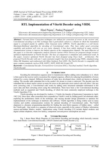
IOSR Journal of VLSI and Signal Processing (IOSR-JVSP) Volume 2, Issue 1 (Mar. – Apr. 2013), PP 65-71 e-ISSN: 2319 – 4200, p-ISSN No. : 2319 – 4197 www.iosrjournals.org RTL Implementation of Viterbi Decoder using VHDL Hiral Pujara 1 , Pankaj Prajapati 2 1 (Electronics &Communication Engineering Department, L.D. College of Engineering/ GTU, India) 2 (Electronics &Communication Engineering Department, L.D. College of Engineering/ GTU, India) Abstract : Forward Error Correction techniques are utilized for correction of errors at the receiver end. Convolutional encoding is an FEC technique that is particularly suited to a channel in which the transmitted signal is corrupted mainly by additive white Gaussian noise (AWGN). Viterbi algorithm is a well known Maximum-likelihood algorithm for decoding of Convolutional codes. They have rather good correcting capability and perform well even on very noisy channels. It has been widely deployed in many wireless communication systems to improve the limited capacity of the communication channels. The main Objective of this paper is to describe comparative analysis between various FPGA Devices for proposed design resource optimized implementation of Viterbi Decoder. The base of comparison is simulation and synthesized result. In this paper, resource optimized Viterbi Decoder has been designed using Trace back architecture. The proposed Viterbi Decoder with rate ½ and constraint Length 3 has been designed using VHDL, simulated using Xilinx ISE Simulator and synthesized with Xilinx Synthesis Tool (XST). The Viterbi Decoder is compatible with many common standards, such as DVB, 3GPP2, 3GPP, IEEE 802.16 and LTE. Keywords - Convolutional Encoder, Forward Error Correction (FEC), Traceback method, Viterbi Algorithm, Viterbi Decoder I. INTRODUCTION Encoding the information sequence prior to transmission implies adding extra redundancy to it, which is then used at the receiver end to reconstruct the original sequence, effectively reducing the probability of errors induced by a noisy channel. Different structures of codes have developed since, which are known as channel coding. The encoder adds redundant bits to the sender's bit stream to create a codeword. The decoder uses the redundant bits to detect and/or correct as many bit errors as the particular error control code will allow. Like any error correcting code, a Convolutional code works by adding some structured redundant information to the user's data and then correcting errors using this information. There have been a few Convolutional decoding methods such as sequential and Viterbi decoding, of which the most commonly employed technique is the Viterbi Algorithm (VA). Viterbi decoding was developed by Andrew. J. Viterbi, the founder of Qualcomm Corporation in April, 1967 [16]. Since then, other researchers have expanded on Viterbi’s work by finding good Convolutional codes, exploring the performance limits of the technique, and varying decoder design parameters to optimize the implementation of the technique in hardware and software. Viterbi algorithm is being widely used in many wireless and mobile communication systems for optimal decoding of Convolutional codes. The Viterbi alignment is a dynamic programming algorithm for finding the most likely sequence of hidden states – called the Viterbi path – that results in a sequence of observed events, especially in the context of Markov information sources and hidden Markov models. Applications using Viterbi decoding [13] include digital modems and digital cellular telephone, where low latency, component cost and power consumption are must. II. VITERBI DECODER Fig. 1 shows Basic Block Diagram of Convolution Encoding and decoding which basically consists three main blocks: Convolutional Encoder, AWGN Channel and Viterbi Decoder [12]. 2.1 Convolutional Encoder x Convolutional c AWGN r Viterbi v Encoder Channel Decoder Noise Figure 1: Block Diagram of Convolution Encoding and Decoding www.iosrjournals.org 65 | Page
- Page 2 and 3: RTL Implementation of Viterbi Decod
- Page 4 and 5: RTL Implementation of Viterbi Decod
- Page 6 and 7: RTL Implementation of Viterbi Decod
<strong>IOSR</strong> Journal <strong>of</strong> VLSI and Signal Processing (<strong>IOSR</strong>-JVSP)<br />
Volume 2, Issue 1 (Mar. – Apr. 2013), PP 65-71<br />
e-ISSN: 2319 – 4200, p-ISSN No. : 2319 – 4197<br />
www.iosrjournals.org<br />
<strong>RTL</strong> <strong>Implementation</strong> <strong>of</strong> <strong>Viterbi</strong> <strong>Decoder</strong> <strong>using</strong> <strong>VHDL</strong><br />
Hiral Pujara 1 , Pankaj Prajapati 2<br />
1 (Electronics &Communication Engineering Department, L.D. College <strong>of</strong> Engineering/ GTU, India)<br />
2 (Electronics &Communication Engineering Department, L.D. College <strong>of</strong> Engineering/ GTU, India)<br />
Abstract : Forward Error Correction techniques are utilized for correction <strong>of</strong> errors at the receiver end.<br />
Convolutional encoding is an FEC technique that is particularly suited to a channel in which the transmitted<br />
signal is corrupted mainly by additive white Gaussian noise (AWGN). <strong>Viterbi</strong> algorithm is a well known<br />
Maximum-likelihood algorithm for decoding <strong>of</strong> Convolutional codes. They have rather good correcting<br />
capability and perform well even on very noisy channels. It has been widely deployed in many wireless<br />
communication systems to improve the limited capacity <strong>of</strong> the communication channels. The main Objective <strong>of</strong><br />
this paper is to describe comparative analysis between various FPGA Devices for proposed design resource<br />
optimized implementation <strong>of</strong> <strong>Viterbi</strong> <strong>Decoder</strong>. The base <strong>of</strong> comparison is simulation and synthesized result. In<br />
this paper, resource optimized <strong>Viterbi</strong> <strong>Decoder</strong> has been designed <strong>using</strong> Trace back architecture. The<br />
proposed <strong>Viterbi</strong> <strong>Decoder</strong> with rate ½ and constraint Length 3 has been designed <strong>using</strong> <strong>VHDL</strong>, simulated <strong>using</strong><br />
Xilinx ISE Simulator and synthesized with Xilinx Synthesis Tool (XST). The <strong>Viterbi</strong> <strong>Decoder</strong> is compatible with<br />
many common standards, such as DVB, 3GPP2, 3GPP, IEEE 802.16 and LTE.<br />
Keywords - Convolutional Encoder, Forward Error Correction (FEC), Traceback method, <strong>Viterbi</strong> Algorithm,<br />
<strong>Viterbi</strong> <strong>Decoder</strong><br />
I. INTRODUCTION<br />
Encoding the information sequence prior to transmission implies adding extra redundancy to it, which<br />
is then used at the receiver end to reconstruct the original sequence, effectively reducing the probability <strong>of</strong> errors<br />
induced by a noisy channel. Different structures <strong>of</strong> codes have developed since, which are known as channel<br />
coding. The encoder adds redundant bits to the sender's bit stream to create a codeword. The decoder uses the<br />
redundant bits to detect and/or correct as many bit errors as the particular error control code will allow. Like any<br />
error correcting code, a Convolutional code works by adding some structured redundant information to the<br />
user's data and then correcting errors <strong>using</strong> this information. There have been a few Convolutional decoding<br />
methods such as sequential and <strong>Viterbi</strong> decoding, <strong>of</strong> which the most commonly employed technique is the<br />
<strong>Viterbi</strong> Algorithm (VA).<br />
<strong>Viterbi</strong> decoding was developed by Andrew. J. <strong>Viterbi</strong>, the founder <strong>of</strong> Qualcomm Corporation in April,<br />
1967 [16]. Since then, other researchers have expanded on <strong>Viterbi</strong>’s work by finding good Convolutional codes,<br />
exploring the performance limits <strong>of</strong> the technique, and varying decoder design parameters to optimize the<br />
implementation <strong>of</strong> the technique in hardware and s<strong>of</strong>tware. <strong>Viterbi</strong> algorithm is being widely used in many<br />
wireless and mobile communication systems for optimal decoding <strong>of</strong> Convolutional codes. The <strong>Viterbi</strong><br />
alignment is a dynamic programming algorithm for finding the most likely sequence <strong>of</strong> hidden states – called<br />
the <strong>Viterbi</strong> path – that results in a sequence <strong>of</strong> observed events, especially in the context <strong>of</strong> Markov information<br />
sources and hidden Markov models. Applications <strong>using</strong> <strong>Viterbi</strong> decoding [13] include digital modems and<br />
digital cellular telephone, where low latency, component cost and power consumption are must.<br />
II. VITERBI DECODER<br />
Fig. 1 shows Basic Block Diagram <strong>of</strong> Convolution Encoding and decoding which basically consists<br />
three main blocks: Convolutional Encoder, AWGN Channel and <strong>Viterbi</strong> <strong>Decoder</strong> [12].<br />
2.1 Convolutional Encoder<br />
x<br />
Convolutional<br />
c<br />
AWGN<br />
r<br />
<strong>Viterbi</strong><br />
v<br />
Encoder<br />
Channel<br />
<strong>Decoder</strong><br />
Noise<br />
Figure 1: Block Diagram <strong>of</strong> Convolution Encoding and Decoding<br />
www.iosrjournals.org<br />
65 | Page
<strong>RTL</strong> <strong>Implementation</strong> <strong>of</strong> <strong>Viterbi</strong> <strong>Decoder</strong> <strong>using</strong> <strong>VHDL</strong><br />
In convolutional encoding n-tuple <strong>of</strong> data is generated for every k-tuple <strong>of</strong> inputs based on both current and K-1<br />
previous k-tuples where K is called constraint length <strong>of</strong> the code. A (n, k, m) convolutional code can be<br />
implemented with a k-input, n-output linear sequential circuit with input memory ‘m’. Typically, ‘n’ and ‘k’ are<br />
small integers with k
<strong>RTL</strong> <strong>Implementation</strong> <strong>of</strong> <strong>Viterbi</strong> <strong>Decoder</strong> <strong>using</strong> <strong>VHDL</strong><br />
1) Branch metric calculation<br />
The first unit is called Branch metric unit. The Hamming distance (or other metric) values we compute<br />
at each time instant for the paths between the states at the previous time instant and the states at the current time<br />
instant are called branch metrics. Hamming distance or Euclidean distance is used for branch metric<br />
computation.<br />
2) Path metric calculation<br />
An accumulated Error metric called path metric (PM) contains the 2 K-1 optimal paths. The current Branch<br />
Metric is added to previous PM and each the two distances are compared for all Add- compare select unit<br />
In terms <strong>of</strong> speed the performance <strong>of</strong> <strong>Viterbi</strong> <strong>Decoder</strong> is mainly determined by the number <strong>of</strong> ACS (2 K-1 )<br />
units and their computation time. As shown in figure each ACS unit comprises two adder blocks, a comparator<br />
and a selector block.<br />
Figure 4: Block Diagram <strong>of</strong> Add Compare Select unit [13]<br />
3) Trace back unit<br />
The final unit is trace back unit where the survivor path and output data are identified. The <strong>Viterbi</strong><br />
decoding flowchart is given in Fig. 5.<br />
Figure 5: <strong>Viterbi</strong> decoding Flow Chart<br />
2.4 Types <strong>of</strong> <strong>Viterbi</strong> Decoding<br />
1) Hard decision <strong>Viterbi</strong> deocding<br />
Demodulator output configured by variety <strong>of</strong> ways [4]: In which output <strong>of</strong> demodulator is quantized into two<br />
levels, zeros and one and fed into decoder (1- bit is used to describe each code symbol). <strong>Decoder</strong> operates on<br />
hard-decisions made by demodulator, decoding is called Hard- decision decoding. In which path through trellis<br />
is determined <strong>using</strong> hamming distance measure.<br />
2) S<strong>of</strong>t decision <strong>Viterbi</strong> deocding<br />
In which output <strong>of</strong> demodulator is quantized into greater than two levels [4]. If output <strong>of</strong> demodulator<br />
is quantized into 3-bit result in 8- level output then 3-bits is used to describe each code symbol. In which<br />
www.iosrjournals.org<br />
67 | Page
<strong>RTL</strong> <strong>Implementation</strong> <strong>of</strong> <strong>Viterbi</strong> <strong>Decoder</strong> <strong>using</strong> <strong>VHDL</strong><br />
Euclidian distance as a distance is measured instead <strong>of</strong> hamming distance. The advantage <strong>of</strong> <strong>using</strong> s<strong>of</strong>t- decision<br />
decoding is to provide decoder with more information, which decoder then use for recovering the message<br />
sequences. It provides better error performance than hard- decision type <strong>Viterbi</strong> decoding also Performance<br />
improvement <strong>of</strong> approximately 2 dB in required S/N ratio compared to two level quantization for a Gaussian<br />
Channel. Disadvantage <strong>of</strong> <strong>using</strong> s<strong>of</strong>t decision decoding is increase in required memory size at decoder and<br />
reduce speed.<br />
2.5 <strong>Viterbi</strong> Decoding Techniques<br />
There are mainly two types <strong>of</strong> decoding techniques available in order to decode the data at the receiver end.<br />
1) Register Exchange Method<br />
In this method, a register assigned to each state contains information bits for the survivor path from the initial<br />
state to current state. In fact, register keeps decoded output sequences along the path. This method requires copy<br />
<strong>of</strong> all registers at each stage. The need to trace back is eliminated since the register <strong>of</strong> final state contains<br />
decoded output sequence. This approach results in complex hardware due to need to copy contents <strong>of</strong> all register<br />
in a stage to next stage. Since the RE method does not need tracing back, it is faster.<br />
2) Traceback Method<br />
Trace back is memory organization method to store survivor paths and retrieve the decoded data. Direct<br />
implementation <strong>of</strong> this method is not practical because <strong>of</strong> an infinite storage size is needed; therefore in practice<br />
semiconductor infinite memory locations are reused periodically. The Trace Back Unit performs three<br />
operations: write new Data, Trace Back Read and Decode Read. Memory is organized as a two dimensional<br />
structure where row are assigned to states and columns to time steps. Three memory blocks are used in<br />
operation: write block is used to store ACS decision vectors, Decode block where the decoded bit sequences is<br />
read in backward order and Trace Back Block which is used to find the starting point <strong>of</strong> next trance back<br />
sequences. Traceback Depth (D) is a predefined parameter that defines the size <strong>of</strong> each memory block [13]. To<br />
guarantee the convergence a traceback depth <strong>of</strong> D = 5K is sufficient and the memory block size will be 2 K-1 x<br />
5K. Traceback method is area efficient and better than RE method. . Register exchange method requires<br />
complex hardware compare to the Traceback method for larger constraint length though it will give faster speed.<br />
In this project I had implemented a hard decision and trace back method for viterbi decoding.<br />
III. PROGRAMMABLE DEVICES<br />
Programmable devices are those devices which can be programmed by the user. Various programmable<br />
devices are PLDs, CPLDs, ASICs and FPGAs.<br />
3.1 Field Programmable Gate Arrays<br />
Field-Programmable Gate Arrays (FPGAs) are pre-fabricated silicon devices that can be electrically<br />
programmed to become almost any kind <strong>of</strong> digital circuit or system. FPGAs contain programmable logic<br />
components called "logic blocks", and a hierarchy <strong>of</strong> reconfigurable interconnects that allow the blocks to be<br />
"wired together"—somewhat like a one-chip programmable breadboard. Logic blocks can be configured to<br />
perform complex combinational functions, or merely simple logic gates like AND and XOR. In most FPGAs,<br />
the logic blocks also include memory elements, which may be simple flip-flops or more complete blocks <strong>of</strong><br />
memory.<br />
They have many advantages over Application Specific Integrated Circuits (ASIC). ASICs are designed<br />
for specific application <strong>using</strong> CAD tools and fabricated at a foundry. Developing an ASIC takes very much time<br />
and is expensive. Furthermore, it is not possible to correct errors after fabrication. In contrast to ASICs, FPGAs<br />
are configured after fabrication and they also can be reconfigured. This is done with a hardware description<br />
language (HDL) which is compiled to a bit stream and downloaded to the FPGA.<br />
The advantages <strong>of</strong> the FPGA approach to CPLD implementation include highest amount <strong>of</strong> logic<br />
density, the most features, and the highest performance. CPLDs, by contrast, <strong>of</strong>fer much smaller amounts <strong>of</strong><br />
logic - up to about 10,000 gates. But CPLDs <strong>of</strong>fer very predictable timing characteristics and are therefore ideal<br />
for critical control applications.<br />
The advantages <strong>of</strong> the FPGA approach to DSP implementation include higher sampling rates than are<br />
available from traditional DSP chips, lower costs than an ASIC. The FPGA also adds design flexibility and<br />
adaptability with optimal device utilization conserving both board space and system power that is <strong>of</strong>ten not the<br />
case with DSP chips. Due to the increase <strong>of</strong> transistor density FPGA were getting more powerful over the years.<br />
Therefore, FPGAs are increasingly applied to high performance embedded systems.<br />
3.2 SPARTAN XC3S400A FPGA<br />
The Spartan®-3A family <strong>of</strong> Field-Programmable Gate Arrays (FPGAs) solves the design challenges in<br />
most high-volume, cost-sensitive, I/O-intensive electronic applications. The five-member family <strong>of</strong>fers<br />
www.iosrjournals.org<br />
68 | Page
<strong>RTL</strong> <strong>Implementation</strong> <strong>of</strong> <strong>Viterbi</strong> <strong>Decoder</strong> <strong>using</strong> <strong>VHDL</strong><br />
densities ranging from 50,000 to 1.4 million system gates. The Spartan-3A FPGAs are part <strong>of</strong> the Extended<br />
Spartan-3A family, which also include the non-volatile Spartan-3AN and the higher density Spartan-3A DSP<br />
FPGAs. The Spartan-3A family builds on the success <strong>of</strong> the earlier Spartan-3E and Spartan-3 FPGA families.<br />
New features improve system performance and reduce the cost <strong>of</strong> configuration. These Spartan-3A family<br />
enhancements, combined with proven 90 nm process technology, deliver more functionality and bandwidth per<br />
dollar than ever before, setting the new standard in the programmable logic industry. Because <strong>of</strong> their<br />
exceptionally low cost, Spartan-3A FPGAs are ideally suited to a wide range <strong>of</strong> consumer electronics<br />
applications, including broadband access, home networking, display/projection, and digital television<br />
equipment. The Spartan-3A family is a superior alternative to mask programmed ASICs. FPGAs avoid the high<br />
initial cost, lengthy development cycles, and the inherent inflexibility <strong>of</strong> conventional ASICs, and permit field<br />
design upgrades.<br />
IV. SOFTWARE USED<br />
Xilinx ISE (Integrated S<strong>of</strong>tware Environment) is a s<strong>of</strong>tware tool produced by Xilinx for synthesis and<br />
analysis <strong>of</strong> HDL designs, which enables the developer to synthesize ("compile") their designs, perform timing<br />
analysis, examine <strong>RTL</strong> diagrams, simulate a design's reaction to different stimuli, and configure the target<br />
device with the programmer. This design is simulated and synthesized <strong>using</strong> Xilinx 10.1 ISE.<br />
4.1 Designing FPGA Devices <strong>using</strong> <strong>VHDL</strong><br />
<strong>VHDL</strong> stands for VHSIC Hardware Description Language. VHSIC is itself an abbreviation for Very<br />
High Speed Integrated Circuits. <strong>VHDL</strong> is hardware description language. It describes behaviour <strong>of</strong> an electronic<br />
system, from which the physical Layer or system can then be implemented. It is intended for circuit synthesis as<br />
well as circuit simulation.<br />
The two main applications immediate <strong>of</strong> <strong>VHDL</strong> are in the field <strong>of</strong> Programmable logic devices and in<br />
the field <strong>of</strong> ASICs. Once the <strong>VHDL</strong> code has been written, it can be used either to implement the circuit in<br />
programmable device or can be submitted to a foundry for fabrication <strong>of</strong> a ASICs chip.<br />
V. SIMULATION AND SYNTHESIS RESULTS<br />
Synthesis is a process <strong>of</strong> constructing a gate level netlist from a register transfer level model <strong>of</strong> a circuit<br />
described in Verilog HDL. Increasing design size and complexity, as well as improvements in design synthesis<br />
and simulation tools, have made Hardware Description Languages (HDLs) the preferred design languages <strong>of</strong><br />
most integrated circuit designers. The two leading HDL synthesis and simulation languages are Verilog and<br />
<strong>VHDL</strong>. Both have been adopted as IEEE standards. The Xilinx ISE s<strong>of</strong>tware is designed to be used with<br />
several HDL synthesis and simulation tools that provide a solution for programmable logic designs from<br />
beginning to end.<br />
5.1 Simulation Waveforms <strong>of</strong> <strong>Viterbi</strong> <strong>Decoder</strong><br />
The Simulation Waveform <strong>of</strong> <strong>Viterbi</strong> <strong>Decoder</strong> is shown in Fig. 6. To observe the speed and resource<br />
utilization, <strong>RTL</strong> is generated, verified and synthesized <strong>using</strong> Xilinx Synthesis Tool (XST).<br />
Figure 6: Simulation Waveform <strong>of</strong> <strong>Viterbi</strong> <strong>Decoder</strong><br />
5.2 <strong>RTL</strong> Schematic <strong>of</strong> <strong>Viterbi</strong> <strong>Decoder</strong><br />
Below Shown is the <strong>RTL</strong> Schematic <strong>of</strong> the <strong>Viterbi</strong> <strong>Decoder</strong>.<br />
www.iosrjournals.org<br />
69 | Page
<strong>RTL</strong> <strong>Implementation</strong> <strong>of</strong> <strong>Viterbi</strong> <strong>Decoder</strong> <strong>using</strong> <strong>VHDL</strong><br />
Figure 7: <strong>RTL</strong> Schematic <strong>of</strong> <strong>Viterbi</strong> <strong>Decoder</strong><br />
5.3 Device Utilization Report<br />
This synthesis report is generated after the compilation <strong>of</strong> Design for the targeted Xilinx SPARTAN<br />
3A based Xc3s400a FPGA Device. Here, The Design unit is not implemented on targeted FPGA Device. This<br />
report contains about component used.<br />
Table 1. Device utilization Summary<br />
5.4 Timing and Power Summary<br />
After the synthesis report, the timing diagram generated according to the given input. With the help <strong>of</strong><br />
timing diagram speed grade, Minimum period, Maximum Frequency, Maximum output required time after<br />
clock is calculated.<br />
Timing Summary<br />
Speed Grade: -4<br />
Minimum period: 30.190ns<br />
Maximum Frequency: 33.124MHz<br />
Minimum input arrival time before clock: 2.993ns<br />
<br />
<br />
Device Utilization Summary<br />
Logic Utilization Used/Available Utilization<br />
Number <strong>of</strong> Slices 104/3584 2 %<br />
Number <strong>of</strong> Slice FFs 95/7168 1 %<br />
Number <strong>of</strong> 4 input 146/7168 2 %<br />
LUTs<br />
Number <strong>of</strong> Bonded 4/195 2 %<br />
IOBs<br />
Number <strong>of</strong> GCLKs 2/24 8 %<br />
Maximum output required time after clock: 5.531ns<br />
Power summary<br />
Total estimated power consumption: P (mw): 49 mw<br />
5.5 Comparative Analysis between Various FPGA Devices<br />
Different FPGA family <strong>of</strong> SPARTAN are used to measure the performance <strong>of</strong> proposed <strong>Viterbi</strong> <strong>Decoder</strong><br />
Design.<br />
5.5.1 Performance Comparison <strong>of</strong> proposed <strong>Viterbi</strong> <strong>Decoder</strong> Design in Various SPARTAN FPGA Devices<br />
Table 2. Comparison between various SPARTAN FPGA Devices<br />
Family Device No. <strong>of</strong> Slices No. <strong>of</strong><br />
Slice FFs.<br />
SPARTAN2<br />
SPARTAN 2E<br />
SPARTAN 3E<br />
SPARTAN<br />
3A<br />
xc2s100<br />
-6fg256<br />
xc2s200e<br />
-7fft256<br />
xc3s500e<br />
-4fg320<br />
xc3s400a<br />
-4fft256<br />
103/1200<br />
(8 %)<br />
104/2352<br />
(4 %)<br />
104/4656<br />
(2 %)<br />
104/3584<br />
(2 %)<br />
95/2400<br />
(3 %)<br />
95/4704<br />
(2 %)<br />
95/9312<br />
(1 %)<br />
95/7168<br />
(1 %)<br />
Total No.<br />
Of<br />
4 i/p LUTs<br />
150/2400<br />
(6 %)<br />
150/4704<br />
(3 %)<br />
143/9312<br />
(1 %)<br />
146/7168<br />
(2 %)<br />
Number<br />
<strong>of</strong><br />
Bonded<br />
IOBs<br />
4/176<br />
(2 %)<br />
4/178<br />
(2 %)<br />
4/232<br />
(1 %)<br />
2/195<br />
(2 %)<br />
Max.<br />
Freq.<br />
22.867<br />
MHz<br />
26.867<br />
MHz<br />
31.512<br />
MHz<br />
33.124<br />
MHz<br />
www.iosrjournals.org<br />
70 | Page
<strong>RTL</strong> <strong>Implementation</strong> <strong>of</strong> <strong>Viterbi</strong> <strong>Decoder</strong> <strong>using</strong> <strong>VHDL</strong><br />
5.5.2 Performance Comparison <strong>of</strong> proposed <strong>Viterbi</strong> <strong>Decoder</strong> Design in Various VIRTEX FPGA Devices<br />
Different FPGA family <strong>of</strong> VIRTEX are used to measure the performance <strong>of</strong> proposed <strong>Viterbi</strong> <strong>Decoder</strong><br />
Design.<br />
Table 3. Comparison between various VIRTEX FPGA Devices<br />
Family Device No. <strong>of</strong> Slices No. <strong>of</strong><br />
Slice FFs.<br />
Virtex 2<br />
Virtex 4<br />
Virtex 5<br />
xc2v500<br />
-6fg256<br />
xc4vlx100<br />
-12ff1148<br />
xc5vlx110<br />
-3ff676<br />
104/3072<br />
(3 %)<br />
105/49152<br />
(0 %)<br />
95/69120<br />
(1 %)<br />
95/6144<br />
(1 %)<br />
95/98304<br />
(0 %)<br />
No. <strong>of</strong> Fully<br />
used LUT-FF<br />
Pair<br />
23/190<br />
(12 %)<br />
Total No.<br />
Of<br />
4 i/p LUTs<br />
142/6144<br />
(2 %)<br />
145/98304<br />
(3 %)<br />
No. <strong>of</strong> Slice<br />
LUT<br />
118/69120<br />
(1 %)<br />
Number<br />
<strong>of</strong><br />
Bonded<br />
IOBs<br />
4/172<br />
(2 %)<br />
4/768<br />
(0 %)<br />
4/440<br />
(0 %)<br />
Max.<br />
Freq.<br />
40.888<br />
MHz<br />
67.057<br />
MHz<br />
113.104<br />
MHz<br />
Virtex E<br />
Xcv400e<br />
-8fg676<br />
103/4800<br />
(2 %)<br />
95/9600<br />
(0 %)<br />
150/9600<br />
(1 %)<br />
4/404<br />
(0 %)<br />
29.933<br />
MHz<br />
VI. CONCLUSIONS<br />
In this Paper Resource optimized <strong>Viterbi</strong> <strong>Decoder</strong> has been proposed. The proposed <strong>Viterbi</strong> <strong>Decoder</strong><br />
has been designed with <strong>VHDL</strong> <strong>using</strong> traceback method. The designed <strong>Viterbi</strong> <strong>Decoder</strong> has been simulated <strong>using</strong><br />
Xilinx ISE simulator and synthesized with XST. The simulated and synthesized results show that proposed<br />
design can work at an estimated frequency <strong>of</strong> 33.124 MHz by <strong>using</strong> considerable less resources <strong>of</strong> target FPGA<br />
device SPARTAN 3A. This Paper also contains comparative analysis between various FPGA devices for the<br />
same Design. The result shows that proposed design can work at Max. Frequency 113.104 MHz for targeted<br />
FPGA Device VIRTEX 5 among all FPGA Devices. So, VRTEX 5 FPGA Device can give Max. Frequency for<br />
proposed Design among all FPGA Devices.<br />
REFERENCES<br />
[1] Mahe Jabeen and Salma Khan, Design <strong>of</strong> Convolution Encoder and Reconfigurable <strong>Viterbi</strong> <strong>Decoder</strong>, International Journal <strong>of</strong><br />
Engineering and Science, Vol. 1, No.3, Sep 2012.<br />
[2] P. Subhashini, D. R. Mahesh Varma and Y. David Solomon Raju, <strong>Implementation</strong> Analysis <strong>of</strong> adaptive <strong>Viterbi</strong> <strong>Decoder</strong> for High<br />
Speed Applications, International Journal <strong>of</strong> Computer Applications (0975-– 8887), Volume 31– No.2, October 2011<br />
[3] S.V.Viraktamath and G.V.Attimarad, Impact <strong>of</strong> constraint length on performance <strong>of</strong> Convolutional Codec in AWGN channel for<br />
image application, International Journal <strong>of</strong> Engineering Science and Technology, Vol. 2(9), 2010, 4696-4700.<br />
[4] Bernard Sklar, Digital Communications Fundamentals and Application, Published by Pearson education, Year 2003<br />
[5] B.P.Lathi, Modern Digital and Analog Communication Systems, Third Edition.<br />
[6] J.G. Proakis, Digital Communications, McGraw Hill.<br />
[7] J. Bhaskar, A <strong>VHDL</strong> Primer, Third Edition<br />
[8] Volnei A. Pedroni, Circuit Design with <strong>VHDL</strong><br />
[9] Christian Baumann, ―Field Programmable Gate Arrray (FPGA), Summary paper for the seminar Embedded System Architecture,<br />
University <strong>of</strong> Innsbruck, January 13, 2010.<br />
[10] Matthias Kamuf, Member, IEEE, Viktor Öwall, Member, IEEE, and John B. Anderson, Fellow, IEEE, Optimization and<br />
<strong>Implementation</strong> <strong>of</strong> a <strong>Viterbi</strong> <strong>Decoder</strong> under Flexibility Constraints, IEEE Transactions on Circuits and Systems—I: Regular<br />
Papers,Vol. 55, No. 8, September 2008.<br />
[11] C. Arun, V. Rajamani, Design and VLSI implementation <strong>of</strong> a Low Probability <strong>of</strong> Error <strong>Viterbi</strong> decoder, First International<br />
Conference on Emerging Trends in Engineering and Technology, IEEE 2008.<br />
[12] Miloš Pilipovic, Marija Tadic, FPGA<strong>Implementation</strong> <strong>of</strong> S<strong>of</strong>t Input <strong>Viterbi</strong> <strong>Decoder</strong> for CDMA2000 System, 16 Th<br />
Telecommunication forum TELEFOR, 2008.<br />
[13] Behzad Mohmad Heravi and Bahram Honary, Multi-rate Parameterized <strong>Viterbi</strong> Decoding for Partial Reconfiguration, PGNet 2006.<br />
[14] Sriram Swaminathan, Russel Tessier, Dennis Goeckel and Wayne Burleson, A Dynamically Reconfigurable Adaptive <strong>Viterbi</strong><br />
<strong>Decoder</strong>, FPGA 02, Feb 2002, pages 24-26.<br />
[15] T. K. Truong, Senior Member IEEE, Ming- Tang Shih, Irving S. Reed, Fellow IEEE, and E.H. Sartorius, Member IEEE, A VLSI<br />
Design for Trace- back <strong>Viterbi</strong> <strong>Decoder</strong>, IEEE Transaction on Communications, Vol. 40, No. 3, March 1992.<br />
[16] A. J. <strong>Viterbi</strong>, Error Bounds for Convolutional Codes and an Asymptotically Optimum Decoding Algorithm, IEEE Trans. Inform<br />
Theory, vol. IT-13, pp. 260-269, Apr. 1967.<br />
www.iosrjournals.org<br />
71 | Page


