Films minces à base de Si nanostructuré pour des cellules ...
Films minces à base de Si nanostructuré pour des cellules ... Films minces à base de Si nanostructuré pour des cellules ...
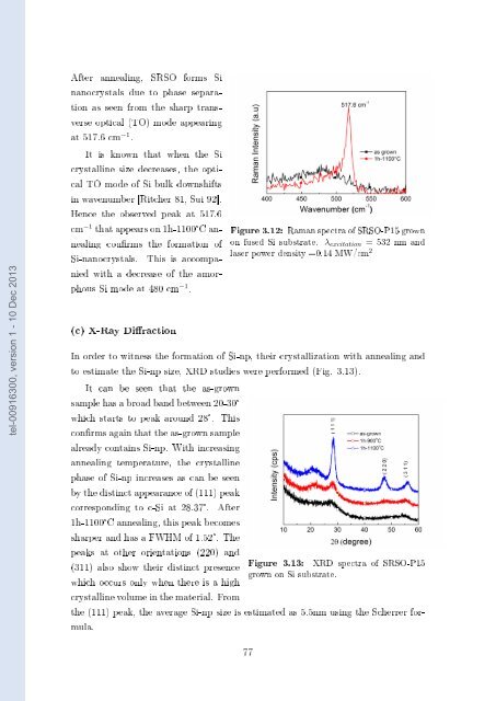
(a) Fourier transform infrared spectroscopy tel-00916300, version 1 - 10 Dec 2013 Figure 3.11 shows the FTIR spectra before and after annealing recorded using Brewster incidence. The inset in this gure shows an enlarged view of the Si-H peak variations with annealing. It can be seen that the LO 3 peak intensity gradually increases with increasing annealing temperatures. Considering the eect of time, for a given temperature 1000°C (1min-1000°C and 1h- 1000°C) there is no signicant change in the LO 3 peak intensity whereas there is a drastic increase when the sample is annealed at 1h-1100°C. This trend represents a gradual evolution towards the phase separation process Figure 3.11: Eect of annealing on the FTIR spectra in Brewster incidence. upon annealing. A gaussian curve tting performed on these spectra indicated a reduction in the peak widths of LO 3 and TO 3 peaks with increasing annealing temperatures. Such reduction in the peak width with increasing annealing treatment has also been observed in [Morales-Sanchez 08] and these changes are attributed to the phase separation processes. In addition, we also notice an increase of the LO 4 −TO 4 mode upon annealing. This indicates the disorder in the matrix due to high Si excess. It can be seen that the Si-H peak appears only in the as-grown sample. The desorption of hydrogen occurs with increasing annealing temperatures leading to a disappearance of this peak. (b) Raman spectroscopy The evolution of Si-np formation between as-grown and 1h-1100°C annealed SRSO- P15 sample as reected by FTIR spectra is conrmed through Raman spectroscopy following the procedure detailed in chapter 2 under section 2.4.4 (Fig. 3.12). It can be seen that the as-grown sample shows a broad peak centered at 480 cm −1 , which decreases in intensity after 1h-1100°C annealing with the appearance of a new peak at 517.6 cm −1 . The Raman spectrum of the as-grown layer shows dominant features of amorphous Si, since SiO 2 is reported to have a very low scattering cross section [Kanzawa 96, Khriachtchev 99]. This conrms the formation of amorphous Si-np in the as-grown sample as indicated by ∼24 at.% of agglomerated Si estimated using ellipsometry (Bruggeman) method (Ref. Tab. 3.6). 76
tel-00916300, version 1 - 10 Dec 2013 After annealing, SRSO forms Si nanocrystals due to phase separation as seen from the sharp transverse optical (TO) mode appearing at 517.6 cm −1 . It is known that when the Si crystalline size decreases, the optical TO mode of Si bulk downshifts in wavenumber [Ritcher 81, Sui 92]. Hence the observed peak at 517.6 cm −1 that appears on 1h-1100°C annealing conrms the formation of Si-nanocrystals. This is accompanied with a decrease of the amorphous Si mode at 480 cm −1 . (c) X-Ray Diraction Figure 3.12: Raman spectra of SRSO-P15 grown on fused Si substrate. λ excitation = 532 nm and laser power density =0.14 MW/cm 2 In order to witness the formation of Si-np, their crystallization with annealing and to estimate the Si-np size, XRD studies were performed (Fig. 3.13). It can be seen that the as-grown sample has a broad band between 20-30° which starts to peak around 28°. This conrms again that the as-grown sample already contains Si-np. With increasing annealing temperature, the crystalline phase of Si-np increases as can be seen by the distinct appearance of (111) peak corresponding to c-Si at 28.37°. After 1h-1100°C annealing, this peak becomes sharper and has a FWHM of 1.52°. The peaks at other orientations (220) and (311) also show their distinct presence which occurs only when there is a high crystalline volume in the material. From Figure 3.13: XRD spectra of SRSO-P15 grown on Si substrate. the (111) peak, the average Si-np size is estimated as 5.5nm using the Scherrer formula. 77
- Page 43 and 44: tel-00916300, version 1 - 10 Dec 20
- Page 45 and 46: Background of this thesis: A new me
- Page 47 and 48: Chapter 2 Experimental techniques a
- Page 49 and 50: maximum power into the plasma. (a)
- Page 51 and 52: Figure 2.2: Illustration of sample
- Page 53 and 54: Ray Diraction, X-Ray Reectivity, El
- Page 55 and 56: (a) Normal Incidence. (b) Oblique (
- Page 57 and 58: to equation 2.4, when X-ray beam st
- Page 59 and 60: investigation. This value is obtain
- Page 61 and 62: e seen that large θ (here, θ is u
- Page 63 and 64: Figure 2.12: Raman spectrometer-Sch
- Page 65 and 66: Experimental set-up and working tel
- Page 67 and 68: ˆ The presence of Si from SiO 2 or
- Page 69 and 70: 2.2.7 Spectroscopic Ellipsometry Pr
- Page 71 and 72: k(E) = f j(ω − ω g ) 2 (ω −
- Page 73 and 74: tel-00916300, version 1 - 10 Dec 20
- Page 75 and 76: Figure 2.20: Schematic diagram of t
- Page 77 and 78: Chapter 3 A study on RF sputtered S
- Page 79 and 80: (a) Deposition rate. (b) Refractive
- Page 81 and 82: Thus, by knowing the refractive ind
- Page 83 and 84: tel-00916300, version 1 - 10 Dec 20
- Page 85 and 86: P Ar (mTorr) P H2 (mTorr) r H (%) 1
- Page 87 and 88: such a peak was witnessed in [Quiro
- Page 89 and 90: the host SiO 2 matrix leading to an
- Page 91 and 92: initiated in this thesis, for the g
- Page 93: P Si (W/cm 2 ) x = 0/Si Bruggemann
- Page 97 and 98: Figure 3.15: Absorption coecient cu
- Page 99 and 100: Aim of the study To see the inuence
- Page 101 and 102: tel-00916300, version 1 - 10 Dec 20
- Page 103 and 104: It can be seen that there is a sign
- Page 105 and 106: tel-00916300, version 1 - 10 Dec 20
- Page 107 and 108: 3.8.4 Inuence of SiO 2 barrier thic
- Page 109 and 110: Chapter 4 A study on RF sputtered S
- Page 111 and 112: 4.2.2 Structural analysis (a) Fouri
- Page 113 and 114: tel-00916300, version 1 - 10 Dec 20
- Page 115 and 116: tel-00916300, version 1 - 10 Dec 20
- Page 117 and 118: tel-00916300, version 1 - 10 Dec 20
- Page 119 and 120: (a) FTIR spectra of NRSN, Si 3 N 4
- Page 121 and 122: tel-00916300, version 1 - 10 Dec 20
- Page 123 and 124: Figure 4.15: Absorption coecient sp
- Page 125 and 126: A multilayer composed of 100 patter
- Page 127 and 128: multilayered conguration. Therefore
- Page 129 and 130: around 1250 cm −1 . The blueshift
- Page 131 and 132: tel-00916300, version 1 - 10 Dec 20
- Page 133 and 134: tion but within a dierence of one o
- Page 135 and 136: sample peak 1 (eV) peak 2 (eV) peak
- Page 137 and 138: (a) 1min annealing vs. T A . (b) 1h
- Page 139 and 140: tel-00916300, version 1 - 10 Dec 20
- Page 141 and 142: (a) Brewster incidence. (b) Normal
- Page 143 and 144: tel-00916300, version 1 - 10 Dec 20
tel-00916300, version 1 - 10 Dec 2013<br />
After annealing, SRSO forms <strong>Si</strong><br />
nanocrystals due to phase separation<br />
as seen from the sharp transverse<br />
optical (TO) mo<strong>de</strong> appearing<br />
at 517.6 cm −1 .<br />
It is known that when the <strong>Si</strong><br />
crystalline size <strong>de</strong>creases, the optical<br />
TO mo<strong>de</strong> of <strong>Si</strong> bulk downshifts<br />
in wavenumber [Ritcher 81, Sui 92].<br />
Hence the observed peak at 517.6<br />
cm −1 that appears on 1h-1100°C annealing<br />
conrms the formation of<br />
<strong>Si</strong>-nanocrystals. This is accompanied<br />
with a <strong>de</strong>crease of the amorphous<br />
<strong>Si</strong> mo<strong>de</strong> at 480 cm −1 .<br />
(c) X-Ray Diraction<br />
Figure 3.12: Raman spectra of SRSO-P15 grown<br />
on fused <strong>Si</strong> substrate. λ excitation = 532 nm and<br />
laser power <strong>de</strong>nsity =0.14 MW/cm 2<br />
In or<strong>de</strong>r to witness the formation of <strong>Si</strong>-np, their crystallization with annealing and<br />
to estimate the <strong>Si</strong>-np size, XRD studies were performed (Fig. 3.13).<br />
It can be seen that the as-grown<br />
sample has a broad band between 20-30°<br />
which starts to peak around 28°. This<br />
conrms again that the as-grown sample<br />
already contains <strong>Si</strong>-np. With increasing<br />
annealing temperature, the crystalline<br />
phase of <strong>Si</strong>-np increases as can be seen<br />
by the distinct appearance of (111) peak<br />
corresponding to c-<strong>Si</strong> at 28.37°. After<br />
1h-1100°C annealing, this peak becomes<br />
sharper and has a FWHM of 1.52°. The<br />
peaks at other orientations (220) and<br />
(311) also show their distinct presence<br />
which occurs only when there is a high<br />
crystalline volume in the material. From<br />
Figure 3.13: XRD spectra of SRSO-P15<br />
grown on <strong>Si</strong> substrate.<br />
the (111) peak, the average <strong>Si</strong>-np size is estimated as 5.5nm using the Scherrer formula.<br />
77


