Films minces à base de Si nanostructuré pour des cellules ...
Films minces à base de Si nanostructuré pour des cellules ... Films minces à base de Si nanostructuré pour des cellules ...
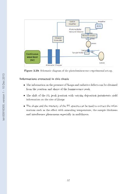
identication of certain defects and impurities. Figure 2.19: Illustration of excitation and de-excitation processes. tel-00916300, version 1 - 10 Dec 2013 Experimental set-up and working The schematic diagram of PL set-up used in our laboratory is as shown in gure 2.20. The optical excitation is provided by a continuous wave Ar laser source (Argon INNOVA CW 90C) operated at 488nm. The laser beam passes through a chopper (Thorlabs MC1000A) set for a chosen frequency (73 Hz). The lock in amplier (SR830) is referenced to the chopper frequency. The laser beam is focussed on the sample at an angle of 45° using appropriate optical lenses. A part of the light emitted by the sample is collected through another set of lenses and is focussed on the entrance slit of the monochromator (TRIAX 180 HORIBA Jobin Yvon). The monochromator disperses the light emitted from the sample and reects towards the exit slit. A photomultiplier tube (PM Vis PL R5108 HAMAMATSU) placed at the exit slit of the monochromator detects the dispersed light. An amplier (AMPLI FEMTO DHPCA-100, DC-200 MHz) amplies the detected signal and converts it into voltage. The signal consisting of all the detected frequencies is fed into the lockin amplier which selects signal at the reference frequency and lter other frequencies (room lighting electrical signal at 50 Hz). All the systems are LABVIEW interfaced. The power of the laser beam at the lm surface was measured using a power meter from LOT-ORIEL. All the PL spectra are standardized to a common reference sample, and corrected to spectral response of the PL set-up. The spectra before and after correcting to spectral response is as shown in gure 2.21. 56
Figure 2.20: Schematic diagram of the photoluminescence experimental set-up. tel-00916300, version 1 - 10 Dec 2013 Informations extracted in this thesis ˆ The information on the presence of Si-nps and radiative defects can be obtained from the position and shape of the luminescence peak. ˆ The shift of the PL peak position with varying deposition parameters yield information on the size of Si-nps ˆ The shape and the intensity of the PL spectra can be used to extract the informations such as the eect with annealing temperature, the sample thickness and interference phenomena especially in multilayers. 57
- Page 23 and 24: Chapter 1 Role of Silicon in Photov
- Page 25 and 26: mono-, poly- and amorphous silicon,
- Page 27 and 28: Figure 1.3: A typical solar cell ar
- Page 29 and 30: occurance of this three body event
- Page 31 and 32: tel-00916300, version 1 - 10 Dec 20
- Page 33 and 34: Shockley-Queisser limit of 31% [Sho
- Page 35 and 36: tel-00916300, version 1 - 10 Dec 20
- Page 37 and 38: tel-00916300, version 1 - 10 Dec 20
- Page 39 and 40: tel-00916300, version 1 - 10 Dec 20
- Page 41 and 42: Figure 1.12: materials. Energy diag
- Page 43 and 44: tel-00916300, version 1 - 10 Dec 20
- Page 45 and 46: Background of this thesis: A new me
- Page 47 and 48: Chapter 2 Experimental techniques a
- Page 49 and 50: maximum power into the plasma. (a)
- Page 51 and 52: Figure 2.2: Illustration of sample
- Page 53 and 54: Ray Diraction, X-Ray Reectivity, El
- Page 55 and 56: (a) Normal Incidence. (b) Oblique (
- Page 57 and 58: to equation 2.4, when X-ray beam st
- Page 59 and 60: investigation. This value is obtain
- Page 61 and 62: e seen that large θ (here, θ is u
- Page 63 and 64: Figure 2.12: Raman spectrometer-Sch
- Page 65 and 66: Experimental set-up and working tel
- Page 67 and 68: ˆ The presence of Si from SiO 2 or
- Page 69 and 70: 2.2.7 Spectroscopic Ellipsometry Pr
- Page 71 and 72: k(E) = f j(ω − ω g ) 2 (ω −
- Page 73: tel-00916300, version 1 - 10 Dec 20
- Page 77 and 78: Chapter 3 A study on RF sputtered S
- Page 79 and 80: (a) Deposition rate. (b) Refractive
- Page 81 and 82: Thus, by knowing the refractive ind
- Page 83 and 84: tel-00916300, version 1 - 10 Dec 20
- Page 85 and 86: P Ar (mTorr) P H2 (mTorr) r H (%) 1
- Page 87 and 88: such a peak was witnessed in [Quiro
- Page 89 and 90: the host SiO 2 matrix leading to an
- Page 91 and 92: initiated in this thesis, for the g
- Page 93 and 94: P Si (W/cm 2 ) x = 0/Si Bruggemann
- Page 95 and 96: tel-00916300, version 1 - 10 Dec 20
- Page 97 and 98: Figure 3.15: Absorption coecient cu
- Page 99 and 100: Aim of the study To see the inuence
- Page 101 and 102: tel-00916300, version 1 - 10 Dec 20
- Page 103 and 104: It can be seen that there is a sign
- Page 105 and 106: tel-00916300, version 1 - 10 Dec 20
- Page 107 and 108: 3.8.4 Inuence of SiO 2 barrier thic
- Page 109 and 110: Chapter 4 A study on RF sputtered S
- Page 111 and 112: 4.2.2 Structural analysis (a) Fouri
- Page 113 and 114: tel-00916300, version 1 - 10 Dec 20
- Page 115 and 116: tel-00916300, version 1 - 10 Dec 20
- Page 117 and 118: tel-00916300, version 1 - 10 Dec 20
- Page 119 and 120: (a) FTIR spectra of NRSN, Si 3 N 4
- Page 121 and 122: tel-00916300, version 1 - 10 Dec 20
- Page 123 and 124: Figure 4.15: Absorption coecient sp
Figure 2.20: Schematic diagram of the photoluminescence experimental set-up.<br />
tel-00916300, version 1 - 10 Dec 2013<br />
Informations extracted in this thesis<br />
ˆ The information on the presence of <strong>Si</strong>-nps and radiative <strong>de</strong>fects can be obtained<br />
from the position and shape of the luminescence peak.<br />
ˆ The shift of the PL peak position with varying <strong>de</strong>position parameters yield<br />
information on the size of <strong>Si</strong>-nps<br />
ˆ The shape and the intensity of the PL spectra can be used to extract the informations<br />
such as the eect with annealing temperature, the sample thickness<br />
and interference phenomena especially in multilayers.<br />
57


