

Films minces à base de Si nanostructuré pour des cellules ...
Films minces à base de Si nanostructuré pour des cellules ...
Films minces à base de Si nanostructuré pour des cellules ...

You also want an ePaper? Increase the reach of your titles
YUMPU automatically turns print PDFs into web optimized ePapers that Google loves.
the values from literatures for band to band recombinations in <strong>Si</strong>-np. Therefore,<br />
the carrier lifetime (τ 34 ) is xed as 50 µs in all the simulations. The time taken for<br />
fast radiative transitions to reach a maximum <strong>de</strong>nsity of excited carriers (τ 23 ) and<br />
the time to <strong>de</strong>excite to ground state (τ 41 ) are xed arbitrarily as 100 and 500 ps<br />
respectively.<br />
5.4.3 Absorption and emission wavelengths<br />
tel-00916300, version 1 - 10 Dec 2013<br />
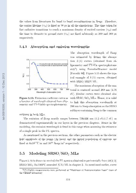
Figure 5.15: Extinction coecient curves as<br />
a function of wavelength obtained from ellipsometry<br />
and UV-Visible spectrophotometry.<br />
The absorption wavelength of <strong>Si</strong>-np<br />
was estimated by tting the absorption<br />
k (λ) curves (obtained from ellipsometry<br />
and UV-Vis spectrophotometry<br />
3 ) using Forouhi-Bloomer mo<strong>de</strong>l<br />
[Forouhi 86]. Figure 5.15 shows the typical<br />
example of k (λ) curves, obtained<br />
with SRSO/SRSN ML.<br />
The maximum absorption of the material<br />
is centered around 260 nm (4.76<br />
eV). <strong>Si</strong>milar curves were obtained also<br />
with SRSO/<strong>Si</strong>O 2 MLs. Hence, it is valid<br />
to link this absorption wavelength at<br />
260 nm to <strong>Si</strong>-np absorption as the SRSO<br />
sublayer containing <strong>Si</strong>-np is the common<br />
sublayer in both MLs.<br />
The emission of <strong>Si</strong>-np mostly ranges between 720-830 nm (1.5 eV-1.7 eV) as<br />
<strong>de</strong>monstrated experimentally in our layers in the previous chapters. Hence in the<br />
mo<strong>de</strong>ling, the emission wavelength is xed in this range when assuming the existence<br />
of a single peak in the PL spectra.<br />
As mentioned in the previous sections, the other parameters such as the electric<br />
eld amplitu<strong>de</strong> of the pump (Ar laser) and the initial population of emitters are<br />
xed at 8x10 3 V/m and 10 26 <strong>Si</strong>-np/m 3 respectively.<br />
5.5 Mo<strong>de</strong>ling SRSO/<strong>Si</strong>O 2 MLs<br />
Figure 5.16 is shown to remind the PL spectra obtained experimentally from 50(3/3)<br />
SRSO/<strong>Si</strong>O 2 1h-1100°C annealed (CA) ML in chapter 3. As mentioned earlier, curve<br />
3 UV-Visible measurements were performed at Matériaux et Instrumentation Laser team of<br />
the CIMAP laboratory<br />
154


