Films minces à base de Si nanostructuré pour des cellules ...
Films minces à base de Si nanostructuré pour des cellules ... Films minces à base de Si nanostructuré pour des cellules ...
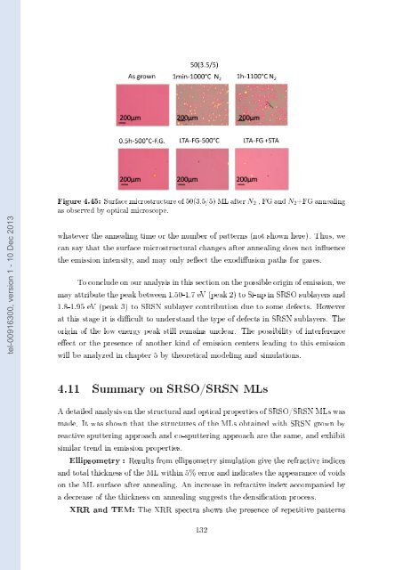
Figure 4.45: Surface microstructure of 50(3.5/5) ML after N 2 , FG and N 2 +FG annealing as observed by optical microscope. tel-00916300, version 1 - 10 Dec 2013 whatever the annealing time or the number of patterns (not shown here). Thus, we can say that the surface microstructural changes after annealing does not inuence the emission intensity, and may only reect the exodiusion paths for gases. To conclude on our analysis in this section on the possible origin of emission, we may attribute the peak between 1.50-1.7 eV (peak 2) to Si-np in SRSO sublayers and 1.8-1.95 eV (peak 3) to SRSN sublayer contribution due to some defects. However at this stage it is dicult to understand the type of defects in SRSN sublayers. The origin of the low energy peak still remains unclear. The possibility of interference eect or the presence of another kind of emission centers leading to this emission will be analyzed in chapter 5 by theoretical modeling and simulations. 4.11 Summary on SRSO/SRSN MLs A detailed analysis on the structural and optical properties of SRSO/SRSN MLs was made. It was shown that the structures of the MLs obtained with SRSN grown by reactive sputtering approach and co-sputtering approach are the same, and exhibit similar trend in emission properties. Ellipsometry : Results from ellipsometry simulation give the refractive indices and total thickness of the ML within 5% error and indicates the appearance of voids on the ML surface after annealing. An increase in refractive index accompanied by a decrease of the thickness on annealing suggests the densication process. XRR and TEM: The XRR spectra shows the presence of repetitive patterns 132
tel-00916300, version 1 - 10 Dec 2013 in the ML and TEM images also reveal a perfect alternation of the SRSO and SRSN sublayers. The pattern thicknesses estimated from XRR and TEM are in agreement with each other thereby demonstrating XRR is a sucient technique to estimate the pattern thickness of a ML. High density of Si-np even after STA (1min-1000 °C/N 2 annealing) is witnessed from HRTEM and EFTEM images. The Si-np are formed only in the SRSO sublayers. FTIR: The combined contribution of the longitudinal and transverse optical modes from SRSO and SRSN sublayers is seen in the FTIR spectra. The blueshift of the Si-N peak indicates an increase in Si-np and nitrogen content with annealing. Similar blueshift and changes in peak intensity associated with the formation of Si-np is observed in the Si-O related bonds. XRD: The investigations on as-grown, STA (1min-1000°C) and CA (1h-1100°C) SRSO/SRSN MLs reveal the presence of Si-np in as-grown state crystallize upon annealing. Absorption coecient : The CA sample has absorption coecient higher than that of as-grown or STA sample over the whole energy range. However, at 3eV the STA sample also possess high α ∼ 10 4 cm −1 comparable to the CA sample. PL: An extensive investigation on the emission behaviour of the ML was made resulting in following observations and understandings: ˆ An interplay between time and temperature of annealing : low time/high temperature (1min-1000°C) & long time/low temperature (16min-700°C) lead to similar PL intensities. Among these STA (1min-1000°C) is identied to be better owing to a lower thermal budget than 16min-700°C. ˆ The highest PL is obtained after STA (1min-1000°C) and almost totally quenched after CA (1h-1100°C). ˆ The highest PL is attributed to the presence of a high density of amorphous clusters, and the quenching is related to the detrimental eect of SRSN sublayers on emission properties with annealing. ˆ Most of the PL spectra can be decomposed into three emission peaks whose origin were investigated. The central peak between 1.5-1.75 eV is attributed to the Si-np 1.9 eV to the defects in SRSN sublayers. The peak at the lower energies is still under investigation and the possible contribution of optical and geometrical eects on this peak is suspected. ˆ The pattern thickness, SRSN sublayer thickness as well as the time spent in the deposition chamber are found to be important factors that control the 133
- Page 99 and 100: Aim of the study To see the inuence
- Page 101 and 102: tel-00916300, version 1 - 10 Dec 20
- Page 103 and 104: It can be seen that there is a sign
- Page 105 and 106: tel-00916300, version 1 - 10 Dec 20
- Page 107 and 108: 3.8.4 Inuence of SiO 2 barrier thic
- Page 109 and 110: Chapter 4 A study on RF sputtered S
- Page 111 and 112: 4.2.2 Structural analysis (a) Fouri
- Page 113 and 114: tel-00916300, version 1 - 10 Dec 20
- Page 115 and 116: tel-00916300, version 1 - 10 Dec 20
- Page 117 and 118: tel-00916300, version 1 - 10 Dec 20
- Page 119 and 120: (a) FTIR spectra of NRSN, Si 3 N 4
- Page 121 and 122: tel-00916300, version 1 - 10 Dec 20
- Page 123 and 124: Figure 4.15: Absorption coecient sp
- Page 125 and 126: A multilayer composed of 100 patter
- Page 127 and 128: multilayered conguration. Therefore
- Page 129 and 130: around 1250 cm −1 . The blueshift
- Page 131 and 132: tel-00916300, version 1 - 10 Dec 20
- Page 133 and 134: tion but within a dierence of one o
- Page 135 and 136: sample peak 1 (eV) peak 2 (eV) peak
- Page 137 and 138: (a) 1min annealing vs. T A . (b) 1h
- Page 139 and 140: tel-00916300, version 1 - 10 Dec 20
- Page 141 and 142: (a) Brewster incidence. (b) Normal
- Page 143 and 144: tel-00916300, version 1 - 10 Dec 20
- Page 145 and 146: increases for the 50 patterned samp
- Page 147 and 148: - Peak (3) and (c): 1.8-1.95 eV Die
- Page 149: 4.10.2 Eect of Si-np Size distribut
- Page 153 and 154: tel-00916300, version 1 - 10 Dec 20
- Page 155 and 156: Chapter 5 Photoluminescence emissio
- Page 157 and 158: As seen from gure 5.1, a part of th
- Page 159 and 160: function of wavelength consists of
- Page 161 and 162: tel-00916300, version 1 - 10 Dec 20
- Page 163 and 164: In the case of our multilayers, the
- Page 165 and 166: ⎛ ⎜ ⎝ A ′ 2 B ′ 2 1 ⎞
- Page 167 and 168: dN 3 dt = N 2 τ 23 − (σ em. φ
- Page 169 and 170: Figure 5.12: The shapes of k(λ) an
- Page 171 and 172: 5.4 Discussion on the choice of inp
- Page 173 and 174: tting operations show the presence
- Page 175 and 176: (a) 270nm. (b) 300nm. tel-00916300,
- Page 177 and 178: (a) σ emis.max. = 8.78 x 10 −18
- Page 179 and 180: (a) 50(3/1.5) (b) 50(3/3) tel-00916
- Page 181 and 182: (a) Integrated population of excite
- Page 183 and 184: two kinds of emitters in SRSO subla
- Page 185 and 186: Conclusion and future perspectives
- Page 187 and 188: 4. Investigating the origin of phot
- Page 189 and 190: Bibliography [Abeles 83] B. Abeles
- Page 191 and 192: [Carlson 76] D. E. Carlson & C. R.
- Page 193 and 194: [Di 10] D. Di, I. Perez-Wur, G. Con
- Page 195 and 196: [Gritsenko 99] V. A. Gritsenko, K.
- Page 197 and 198: [Kaiser 56] W. Kaiser, P. H. Kech &
- Page 199 and 200: [Mandelkorn 62] J. Mandelkorn, C. M
Figure 4.45: Surface microstructure of 50(3.5/5) ML after N 2 , FG and N 2 +FG annealing<br />
as observed by optical microscope.<br />
tel-00916300, version 1 - 10 Dec 2013<br />
whatever the annealing time or the number of patterns (not shown here). Thus, we<br />
can say that the surface microstructural changes after annealing does not inuence<br />
the emission intensity, and may only reect the exodiusion paths for gases.<br />
To conclu<strong>de</strong> on our analysis in this section on the possible origin of emission, we<br />
may attribute the peak between 1.50-1.7 eV (peak 2) to <strong>Si</strong>-np in SRSO sublayers and<br />
1.8-1.95 eV (peak 3) to SRSN sublayer contribution due to some <strong>de</strong>fects. However<br />
at this stage it is dicult to un<strong>de</strong>rstand the type of <strong>de</strong>fects in SRSN sublayers. The<br />
origin of the low energy peak still remains unclear. The possibility of interference<br />
eect or the presence of another kind of emission centers leading to this emission<br />
will be analyzed in chapter 5 by theoretical mo<strong>de</strong>ling and simulations.<br />
4.11 Summary on SRSO/SRSN MLs<br />
A <strong>de</strong>tailed analysis on the structural and optical properties of SRSO/SRSN MLs was<br />
ma<strong>de</strong>. It was shown that the structures of the MLs obtained with SRSN grown by<br />
reactive sputtering approach and co-sputtering approach are the same, and exhibit<br />
similar trend in emission properties.<br />
Ellipsometry : Results from ellipsometry simulation give the refractive indices<br />
and total thickness of the ML within 5% error and indicates the appearance of voids<br />
on the ML surface after annealing. An increase in refractive in<strong>de</strong>x accompanied by<br />
a <strong>de</strong>crease of the thickness on annealing suggests the <strong>de</strong>nsication process.<br />
XRR and TEM: The XRR spectra shows the presence of repetitive patterns<br />
132


