

Films minces à base de Si nanostructuré pour des cellules ...
Films minces à base de Si nanostructuré pour des cellules ...
Films minces à base de Si nanostructuré pour des cellules ...

Create successful ePaper yourself
Turn your PDF publications into a flip-book with our unique Google optimized e-Paper software.
samples from atmosphere since this shoul<strong>de</strong>r lies at the (TO 3 ) <strong>Si</strong>−O peak position.<br />
The inset of gure 4.4 shows that the spectra recor<strong>de</strong>d in the normal inci<strong>de</strong>nce<br />
also exhibits a similar behaviour with annealing. There is a shift of the TO mo<strong>de</strong><br />
between 843-864 cm −1 indicating a rearrangement of the <strong>Si</strong> and N atoms. The TO<br />
peak after CA shows an increased width which is attributed to an overlapping of<br />
TO <strong>Si</strong>−N with (TO 3 ) <strong>Si</strong>−O mo<strong>de</strong>s due to oxidation.<br />
(b) X-Ray Diraction<br />
tel-00916300, version 1 - 10 Dec 2013<br />
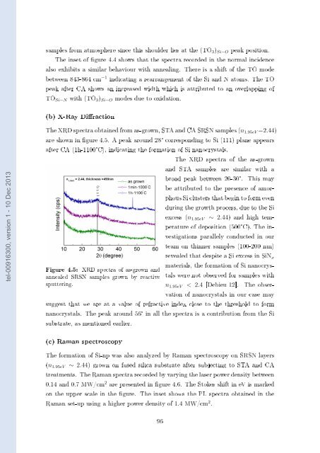
The XRD spectra obtained from as-grown, STA and CA SRSN samples (n 1.95eV =2.44)<br />
are shown in gure 4.5. A peak around 28° corresponding to <strong>Si</strong> (111) plane appears<br />
after CA (1h-1100°C), indicating the formation of <strong>Si</strong> nanocrystals.<br />
The XRD spectra of the as-grown<br />
and STA samples are similar with a<br />
broad peak between 20-30°. This may<br />
be attributed to the presence of amorphous<br />
<strong>Si</strong> clusters that begin to form even<br />
during the growth process, due to the <strong>Si</strong><br />
Figure 4.5: XRD spectra of as-grown and<br />
annealed SRSN samples grown by reactive<br />
sputtering.<br />
excess (n 1.95eV ∼ 2.44) and high temperature<br />
of <strong>de</strong>position (500°C). The investigations<br />
parallely conducted in our<br />
team on thinner samples (100-200 nm)<br />
revealed that <strong>de</strong>spite a <strong>Si</strong> excess in <strong>Si</strong>N x<br />
materials, the formation of <strong>Si</strong> nanocrystals<br />
were not observed for samples with<br />
n 1.95eV < 2.4 [Debieu 12]. The observation<br />
of nanocrystals in our case may<br />
suggest that we are at a value of refractive in<strong>de</strong>x close to the threshold to form<br />
nanocrystals. The peak around 56° in all the spectra is a contribution from the <strong>Si</strong><br />
substrate, as mentioned earlier.<br />
(c) Raman spectroscopy<br />
The formation of <strong>Si</strong>-np was also analyzed by Raman spectroscopy on SRSN layers<br />
(n 1.95eV ∼ 2.44) grown on fused silica substrate after subjecting to STA and CA<br />
treatments. The Raman spectra recor<strong>de</strong>d by varying the laser power <strong>de</strong>nsity between<br />
0.14 and 0.7 MW/cm 2 are presented in gure 4.6. The Stokes shift in eV is marked<br />
on the upper scale in the gure. The inset shows the PL spectra obtained in the<br />
Raman set-up using a higher power <strong>de</strong>nsity of 1.4 MW/cm 2 .<br />
96


