Films minces à base de Si nanostructuré pour des cellules ...
Films minces à base de Si nanostructuré pour des cellules ... Films minces à base de Si nanostructuré pour des cellules ...
4.2 N 2 -Reactive sputtering of Si cathode The SiN x layers were grown by sputtering Si cathode in a nitrogen rich plasma. The RF power density applied on the Si cathode (P Si ) and the time of deposition were xed at 4.44 W/cm 2 and 3600s respectively. The reactive gas rate r N was varied between 5.1%-16% in order to change the composition of the material (as indicated by the refractive indices) between stochiometric and Si-rich SiN x layers. Table 4.1 details the conditions used in this thesis, for obtaining N 2 -rich plasma. tel-00916300, version 1 - 10 Dec 2013 P Ar (mTorr) P N2 (mTorr) r N (%) 14.8 0.8 5.1 14.1 1.1 7.1 14 1.5 9.6 13.6 1.9 12 12.8 2.5 16 Table 4.1: Conditions used to obtain N 2 − rich plasma. 4.2.1 Refractive index (n 1.95eV ) and Deposition rates (r d ) Figure 4.1 shows n 1.95eV and r d of the samples with regard to r N . Figure 4.1: Eect of r N on refractive index (left axis) and deposition rate (right axis). The refractive indices increase with decreasing r N , thereby making the material Si-rich. It can be seen that by varying r N , n 1.95eV changes between 2.01 to 3.3 which indicates that the composition can be tuned between Si 3 N 4 and Si. The deposition rate can be seen to decrease with increasing r N . This is attributed to the diculty in sputtering the target when r N is high, as observed in other sputtering set-ups in our team as well. The value, n 1.95eV ∼ 2.4 was chosen for most of the MLs to obtain a SRSN sublayer. 92
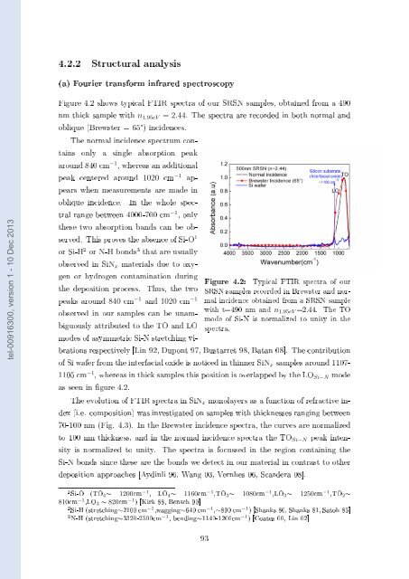
4.2.2 Structural analysis (a) Fourier transform infrared spectroscopy tel-00916300, version 1 - 10 Dec 2013 Figure 4.2 shows typical FTIR spectra of our SRSN samples, obtained from a 490 nm thick sample with n 1.95eV = 2.44. The spectra are recorded in both normal and oblique (Brewster = 65°) incidences. The normal incidence spectrum contains only a single absorption peak around 840 cm −1 , whereas an additional peak centered around 1020 cm −1 appears when measurements are made in Figure 4.2: Typical FTIR spectra of our SRSN samples recorded in Brewster and normal incidence obtained from a SRSN sample with t=490 nm and n 1.95eV =2.44. The TO mode of Si-N is normalized to unity in the spectra. oblique incidence. In the whole spectral range between 4000-700 cm −1 , only these two absorption bands can be observed. This proves the absence of Si-O 1 or Si-H 2 or N-H bonds 3 that are usually observed in SiN x materials due to oxygen or hydrogen contamination during the deposition process. Thus, the two peaks around 840 cm −1 and 1020 cm −1 observed in our samples can be unambiguously attributed to the TO and LO modes of asymmetric Si-N stretching vibrations respectively [Lin 92, Dupont 97, Bustarret 98, Batan 08]. The contribution of Si wafer from the interfacial oxide is noticed in thinner SiN x samples around 1107- 1105 cm −1 , whereas in thick samples this position is overlapped by the LO Si−N mode as seen in gure 4.2. The evolution of FTIR spectra in SiN x monolayers as a function of refractive index (i.e. composition) was investigated on samples with thicknesses ranging between 70-100 nm (Fig. 4.3). In the Brewster incidence spectra, the curves are normalized to 100 nm thickness, and in the normal incidence spectra the TO Si−N peak intensity is normalized to unity. The spectra is focussed in the region containing the Si-N bonds since these are the bonds we detect in our material in contrast to other deposition approaches [Aydinli 96, Wang 03, Vernhes 06, Scardera 08]. 1 Si-O (TO 4 ∼ 1200cm −1 , LO 4 ∼ 1160cm −1 ,TO 3 ∼ 1080cm −1 ,LO 3 ∼ 1250cm −1 ,TO 2 ∼ 810cm −1 ,LO 3 ∼ 820cm −1 ) [Kirk 88, Bensch 90] 2 Si-H (stretching∼2100 cm −1 ,wagging∼640 cm −1 ,∼890 cm −1 ) [Shanks 80, Shanks 81, Satoh 85] 3 N-H (stretching∼3320-2500cm −1 , bending∼1140-1200cm −1 ) [Coates 00, Lin 02] 93
- Page 59 and 60: investigation. This value is obtain
- Page 61 and 62: e seen that large θ (here, θ is u
- Page 63 and 64: Figure 2.12: Raman spectrometer-Sch
- Page 65 and 66: Experimental set-up and working tel
- Page 67 and 68: ˆ The presence of Si from SiO 2 or
- Page 69 and 70: 2.2.7 Spectroscopic Ellipsometry Pr
- Page 71 and 72: k(E) = f j(ω − ω g ) 2 (ω −
- Page 73 and 74: tel-00916300, version 1 - 10 Dec 20
- Page 75 and 76: Figure 2.20: Schematic diagram of t
- Page 77 and 78: Chapter 3 A study on RF sputtered S
- Page 79 and 80: (a) Deposition rate. (b) Refractive
- Page 81 and 82: Thus, by knowing the refractive ind
- Page 83 and 84: tel-00916300, version 1 - 10 Dec 20
- Page 85 and 86: P Ar (mTorr) P H2 (mTorr) r H (%) 1
- Page 87 and 88: such a peak was witnessed in [Quiro
- Page 89 and 90: the host SiO 2 matrix leading to an
- Page 91 and 92: initiated in this thesis, for the g
- Page 93 and 94: P Si (W/cm 2 ) x = 0/Si Bruggemann
- Page 95 and 96: tel-00916300, version 1 - 10 Dec 20
- Page 97 and 98: Figure 3.15: Absorption coecient cu
- Page 99 and 100: Aim of the study To see the inuence
- Page 101 and 102: tel-00916300, version 1 - 10 Dec 20
- Page 103 and 104: It can be seen that there is a sign
- Page 105 and 106: tel-00916300, version 1 - 10 Dec 20
- Page 107 and 108: 3.8.4 Inuence of SiO 2 barrier thic
- Page 109: Chapter 4 A study on RF sputtered S
- Page 113 and 114: tel-00916300, version 1 - 10 Dec 20
- Page 115 and 116: tel-00916300, version 1 - 10 Dec 20
- Page 117 and 118: tel-00916300, version 1 - 10 Dec 20
- Page 119 and 120: (a) FTIR spectra of NRSN, Si 3 N 4
- Page 121 and 122: tel-00916300, version 1 - 10 Dec 20
- Page 123 and 124: Figure 4.15: Absorption coecient sp
- Page 125 and 126: A multilayer composed of 100 patter
- Page 127 and 128: multilayered conguration. Therefore
- Page 129 and 130: around 1250 cm −1 . The blueshift
- Page 131 and 132: tel-00916300, version 1 - 10 Dec 20
- Page 133 and 134: tion but within a dierence of one o
- Page 135 and 136: sample peak 1 (eV) peak 2 (eV) peak
- Page 137 and 138: (a) 1min annealing vs. T A . (b) 1h
- Page 139 and 140: tel-00916300, version 1 - 10 Dec 20
- Page 141 and 142: (a) Brewster incidence. (b) Normal
- Page 143 and 144: tel-00916300, version 1 - 10 Dec 20
- Page 145 and 146: increases for the 50 patterned samp
- Page 147 and 148: - Peak (3) and (c): 1.8-1.95 eV Die
- Page 149 and 150: 4.10.2 Eect of Si-np Size distribut
- Page 151 and 152: tel-00916300, version 1 - 10 Dec 20
- Page 153 and 154: tel-00916300, version 1 - 10 Dec 20
- Page 155 and 156: Chapter 5 Photoluminescence emissio
- Page 157 and 158: As seen from gure 5.1, a part of th
- Page 159 and 160: function of wavelength consists of
4.2.2 Structural analysis<br />
(a) Fourier transform infrared spectroscopy<br />
tel-00916300, version 1 - 10 Dec 2013<br />
Figure 4.2 shows typical FTIR spectra of our SRSN samples, obtained from a 490<br />
nm thick sample with n 1.95eV = 2.44. The spectra are recor<strong>de</strong>d in both normal and<br />
oblique (Brewster = 65°) inci<strong>de</strong>nces.<br />
The normal inci<strong>de</strong>nce spectrum contains<br />
only a single absorption peak<br />
around 840 cm −1 , whereas an additional<br />
peak centered around 1020 cm −1 appears<br />
when measurements are ma<strong>de</strong> in<br />
Figure 4.2: Typical FTIR spectra of our<br />
SRSN samples recor<strong>de</strong>d in Brewster and normal<br />
inci<strong>de</strong>nce obtained from a SRSN sample<br />
with t=490 nm and n 1.95eV =2.44. The TO<br />
mo<strong>de</strong> of <strong>Si</strong>-N is normalized to unity in the<br />
spectra.<br />
oblique inci<strong>de</strong>nce. In the whole spectral<br />
range between 4000-700 cm −1 , only<br />
these two absorption bands can be observed.<br />
This proves the absence of <strong>Si</strong>-O 1<br />
or <strong>Si</strong>-H 2 or N-H bonds 3 that are usually<br />
observed in <strong>Si</strong>N x materials due to oxygen<br />
or hydrogen contamination during<br />
the <strong>de</strong>position process. Thus, the two<br />
peaks around 840 cm −1 and 1020 cm −1<br />
observed in our samples can be unambiguously<br />
attributed to the TO and LO<br />
mo<strong>de</strong>s of asymmetric <strong>Si</strong>-N stretching vibrations<br />
respectively [Lin 92, Dupont 97, Bustarret 98, Batan 08]. The contribution<br />
of <strong>Si</strong> wafer from the interfacial oxi<strong>de</strong> is noticed in thinner <strong>Si</strong>N x samples around 1107-<br />
1105 cm −1 , whereas in thick samples this position is overlapped by the LO <strong>Si</strong>−N mo<strong>de</strong><br />
as seen in gure 4.2.<br />
The evolution of FTIR spectra in <strong>Si</strong>N x monolayers as a function of refractive in<strong>de</strong>x<br />
(i.e. composition) was investigated on samples with thicknesses ranging between<br />
70-100 nm (Fig. 4.3). In the Brewster inci<strong>de</strong>nce spectra, the curves are normalized<br />
to 100 nm thickness, and in the normal inci<strong>de</strong>nce spectra the TO <strong>Si</strong>−N peak intensity<br />
is normalized to unity. The spectra is focussed in the region containing the<br />
<strong>Si</strong>-N bonds since these are the bonds we <strong>de</strong>tect in our material in contrast to other<br />
<strong>de</strong>position approaches [Aydinli 96, Wang 03, Vernhes 06, Scar<strong>de</strong>ra 08].<br />
1 <strong>Si</strong>-O (TO 4 ∼ 1200cm −1 , LO 4 ∼ 1160cm −1 ,TO 3 ∼ 1080cm −1 ,LO 3 ∼ 1250cm −1 ,TO 2 ∼<br />
810cm −1 ,LO 3 ∼ 820cm −1 ) [Kirk 88, Bensch 90]<br />
2 <strong>Si</strong>-H (stretching∼2100 cm −1 ,wagging∼640 cm −1 ,∼890 cm −1 ) [Shanks 80, Shanks 81, Satoh 85]<br />
3 N-H (stretching∼3320-2500cm −1 , bending∼1140-1200cm −1 ) [Coates 00, Lin 02]<br />
93


