Films minces à base de Si nanostructuré pour des cellules ...
Films minces à base de Si nanostructuré pour des cellules ... Films minces à base de Si nanostructuré pour des cellules ...
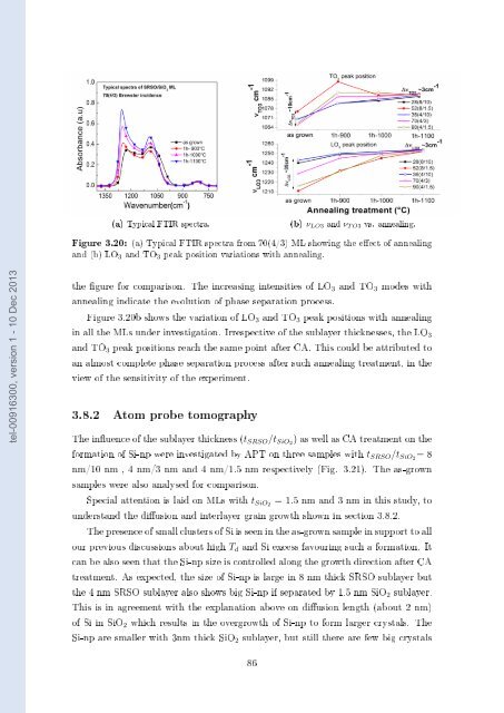
(a) Typical FTIR spectra. (b) ν LO3 and ν T O3 vs. annealing. Figure 3.20: (a) Typical FTIR spectra from 70(4/3) ML showing the eect of annealing and (b) LO 3 and TO 3 peak position variations with annealing. tel-00916300, version 1 - 10 Dec 2013 the gure for comparison. The increasing intensities of LO 3 and TO 3 modes with annealing indicate the evolution of phase separation process. Figure 3.20b shows the variation of LO 3 and TO 3 peak positions with annealing in all the MLs under investigation. Irrespective of the sublayer thicknesses, the LO 3 and TO 3 peak positions reach the same point after CA. This could be attributed to an almost complete phase separation process after such annealing treatment, in the view of the sensitivity of the experiment. 3.8.2 Atom probe tomography The inuence of the sublayer thickness (t SRSO /t SiO2 ) as well as CA treatment on the formation of Si-np were investigated by APT on three samples with t SRSO /t SiO2 = 8 nm/10 nm , 4 nm/3 nm and 4 nm/1.5 nm respectively (Fig. 3.21). The as-grown samples were also analysed for comparison. Special attention is laid on MLs with t SiO2 = 1.5 nm and 3 nm in this study, to understand the diusion and interlayer grain growth shown in section 3.8.2. The presence of small clusters of Si is seen in the as-grown sample in support to all our previous discussions about high T d and Si excess favouring such a formation. It can be also seen that the Si-np size is controlled along the growth direction after CA treatment. As expected, the size of Si-np is large in 8 nm thick SRSO sublayer but the 4 nm SRSO sublayer also shows big Si-np if separated by 1.5 nm SiO 2 sublayer. This is in agreement with the explanation above on diusion length (about 2 nm) of Si in SiO 2 which results in the overgrowth of Si-np to form larger crystals. The Si-np are smaller with 3nm thick SiO 2 sublayer, but still there are few big crystals 86
tel-00916300, version 1 - 10 Dec 2013 Figure 3.21: Inuence of sublayer thicknesses on Si-np formation. Upper part of the gure shows the plan view of Si-np in SiO x sublayers in as-grown and CA cases with regard to sublayer thickness. The bottom part of the gure shows a 3D illustration and a 3D volumic reconstruction of two specic cases of ML. (The plan view and volumic reconstructed images are given by M. Roussel from GPM). as seen in 70(4/3) case (Fig. 3.21). These results conrm that the SiO 2 sublayer plays a strong role as a barrier layer in the formation of Si-np with controlled sizes. 3.8.3 Photoluminescence The PL spectra of the samples after CA are shown in gure 3.22. In gure 3.22a the spectra are as recorded and in gure 3.22b the spectra is normalized to the pattern number. As mentioned before, all the curves are corrected to spectral response. It can be seen in both the gures that there is no emission if t SRSO = 8 nm which is attributed to the overgrowth of Si-np resulting in the loss of quantum connement. In gure 3.22a it can be noticed that the most intense emission is obtained from 70(4/3) ML. Considering the MLs with 4 nm thick SRSO sublayers, we observe the lowest intensity for the highest number of emitters (green curve) and the highest emission for the intermediate number of emitters (pink curve). Consequently the number of emitters is not the only necessary parameter to achieve the highest intensity. This non-monotonous trend must be considered along with the t SiO2 which may play a role on the emission intensity. Since the total thickness of these samples are the same, the relevant parameter to compare the spectra would be to nomalize to one pattern of each ML. Therefore in 87
- Page 53 and 54: Ray Diraction, X-Ray Reectivity, El
- Page 55 and 56: (a) Normal Incidence. (b) Oblique (
- Page 57 and 58: to equation 2.4, when X-ray beam st
- Page 59 and 60: investigation. This value is obtain
- Page 61 and 62: e seen that large θ (here, θ is u
- Page 63 and 64: Figure 2.12: Raman spectrometer-Sch
- Page 65 and 66: Experimental set-up and working tel
- Page 67 and 68: ˆ The presence of Si from SiO 2 or
- Page 69 and 70: 2.2.7 Spectroscopic Ellipsometry Pr
- Page 71 and 72: k(E) = f j(ω − ω g ) 2 (ω −
- Page 73 and 74: tel-00916300, version 1 - 10 Dec 20
- Page 75 and 76: Figure 2.20: Schematic diagram of t
- Page 77 and 78: Chapter 3 A study on RF sputtered S
- Page 79 and 80: (a) Deposition rate. (b) Refractive
- Page 81 and 82: Thus, by knowing the refractive ind
- Page 83 and 84: tel-00916300, version 1 - 10 Dec 20
- Page 85 and 86: P Ar (mTorr) P H2 (mTorr) r H (%) 1
- Page 87 and 88: such a peak was witnessed in [Quiro
- Page 89 and 90: the host SiO 2 matrix leading to an
- Page 91 and 92: initiated in this thesis, for the g
- Page 93 and 94: P Si (W/cm 2 ) x = 0/Si Bruggemann
- Page 95 and 96: tel-00916300, version 1 - 10 Dec 20
- Page 97 and 98: Figure 3.15: Absorption coecient cu
- Page 99 and 100: Aim of the study To see the inuence
- Page 101 and 102: tel-00916300, version 1 - 10 Dec 20
- Page 103: It can be seen that there is a sign
- Page 107 and 108: 3.8.4 Inuence of SiO 2 barrier thic
- Page 109 and 110: Chapter 4 A study on RF sputtered S
- Page 111 and 112: 4.2.2 Structural analysis (a) Fouri
- Page 113 and 114: tel-00916300, version 1 - 10 Dec 20
- Page 115 and 116: tel-00916300, version 1 - 10 Dec 20
- Page 117 and 118: tel-00916300, version 1 - 10 Dec 20
- Page 119 and 120: (a) FTIR spectra of NRSN, Si 3 N 4
- Page 121 and 122: tel-00916300, version 1 - 10 Dec 20
- Page 123 and 124: Figure 4.15: Absorption coecient sp
- Page 125 and 126: A multilayer composed of 100 patter
- Page 127 and 128: multilayered conguration. Therefore
- Page 129 and 130: around 1250 cm −1 . The blueshift
- Page 131 and 132: tel-00916300, version 1 - 10 Dec 20
- Page 133 and 134: tion but within a dierence of one o
- Page 135 and 136: sample peak 1 (eV) peak 2 (eV) peak
- Page 137 and 138: (a) 1min annealing vs. T A . (b) 1h
- Page 139 and 140: tel-00916300, version 1 - 10 Dec 20
- Page 141 and 142: (a) Brewster incidence. (b) Normal
- Page 143 and 144: tel-00916300, version 1 - 10 Dec 20
- Page 145 and 146: increases for the 50 patterned samp
- Page 147 and 148: - Peak (3) and (c): 1.8-1.95 eV Die
- Page 149 and 150: 4.10.2 Eect of Si-np Size distribut
- Page 151 and 152: tel-00916300, version 1 - 10 Dec 20
- Page 153 and 154: tel-00916300, version 1 - 10 Dec 20
(a) Typical FTIR spectra.<br />
(b) ν LO3 and ν T O3 vs. annealing.<br />
Figure 3.20: (a) Typical FTIR spectra from 70(4/3) ML showing the eect of annealing<br />
and (b) LO 3 and TO 3 peak position variations with annealing.<br />
tel-00916300, version 1 - 10 Dec 2013<br />
the gure for comparison. The increasing intensities of LO 3 and TO 3 mo<strong>de</strong>s with<br />
annealing indicate the evolution of phase separation process.<br />
Figure 3.20b shows the variation of LO 3 and TO 3 peak positions with annealing<br />
in all the MLs un<strong>de</strong>r investigation. Irrespective of the sublayer thicknesses, the LO 3<br />
and TO 3 peak positions reach the same point after CA. This could be attributed to<br />
an almost complete phase separation process after such annealing treatment, in the<br />
view of the sensitivity of the experiment.<br />
3.8.2 Atom probe tomography<br />
The inuence of the sublayer thickness (t SRSO /t <strong>Si</strong>O2 ) as well as CA treatment on the<br />
formation of <strong>Si</strong>-np were investigated by APT on three samples with t SRSO /t <strong>Si</strong>O2 = 8<br />
nm/10 nm , 4 nm/3 nm and 4 nm/1.5 nm respectively (Fig. 3.21). The as-grown<br />
samples were also analysed for comparison.<br />
Special attention is laid on MLs with t <strong>Si</strong>O2 = 1.5 nm and 3 nm in this study, to<br />
un<strong>de</strong>rstand the diusion and interlayer grain growth shown in section 3.8.2.<br />
The presence of small clusters of <strong>Si</strong> is seen in the as-grown sample in support to all<br />
our previous discussions about high T d and <strong>Si</strong> excess favouring such a formation. It<br />
can be also seen that the <strong>Si</strong>-np size is controlled along the growth direction after CA<br />
treatment. As expected, the size of <strong>Si</strong>-np is large in 8 nm thick SRSO sublayer but<br />
the 4 nm SRSO sublayer also shows big <strong>Si</strong>-np if separated by 1.5 nm <strong>Si</strong>O 2 sublayer.<br />
This is in agreement with the explanation above on diusion length (about 2 nm)<br />
of <strong>Si</strong> in <strong>Si</strong>O 2 which results in the overgrowth of <strong>Si</strong>-np to form larger crystals. The<br />
<strong>Si</strong>-np are smaller with 3nm thick <strong>Si</strong>O 2 sublayer, but still there are few big crystals<br />
86


