Films minces à base de Si nanostructuré pour des cellules ...
Films minces à base de Si nanostructuré pour des cellules ... Films minces à base de Si nanostructuré pour des cellules ...
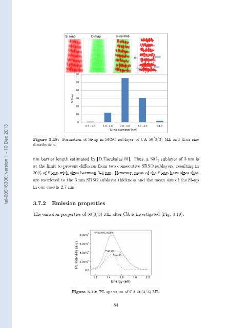
tel-00916300, version 1 - 10 Dec 2013 Figure 3.18: distribution. Formation of Si-np in SRSO sublayer of CA 50(3/3) ML and their size nm barrier length estimated by [D.Tsoukalas 01]. Thus, a SiO 2 sublayer of 3 nm is at the limit to prevent diusion from two consecutive SRSO sublayers, resulting in 30% of Si-np with sizes between 3-4 nm. However, most of the Si-np have sizes that are restricted to the 3 nm SRSO sublayer thickness and the mean size of the Si-np in our case is 2.7 nm. 3.7.2 Emission properties The emission properties of 50(3/3) ML after CA is investigated (Fig. 3.19). Figure 3.19: PL spectrum of CA 50(3/3) ML. 84
It can be seen that there is a signicant emission from the material in the visible range, contrary to the absence of any emission in SRSO-P15 monolayer. This con- rms that the absence of emission in a monolayered conguration at this annealing is due to the loss of quantum connement of carriers. The agglomeration into big size particles is prevented in the ML leading to this emission. It is interesting to note that the curve is composed of two peaks, peak (1) and peak (2) at 1.41 eV and 1.53 eV respectively indicating there are more than one type of emitters. We can attribute the peak at higher energy (1.53 eV) to Si-np whose sizes range between 2-3 nm, which represent more than 50% of Si-np (ref. Fig. 3.18), since the mean size of our Si-np are only about 2.7 nm and cannot lead to a redshifted emission. Peak (1) at lower energy (1.41 eV) might be attributed to bigger sized particles that are formed due to overgrowth at interfaces as observed in APT. tel-00916300, version 1 - 10 Dec 2013 3.8 Inuence of sublayer thicknesses In order to further explore the emission properties, the inuence of the SRSO and the SiO 2 sublayer thicknesses on the formation of Si-np becomes the next subject of concern. To begin our investigations, ve MLs with dierent thicknesses of SRSO and SiO 2 sublayers were grown as detailed in table 3.8. The total thickness of the samples were xed around 500 nm to ensure uniformity in comparison. Since this part of the study is shared between this thesis and the thesis of M. Roussel 4 , these sublayer thicknesses were chosen to suit the needs of both. Notation Patterns t SRSO (nm) t SiO2 (nm) Total thickness (nm) 28(8/10) 28 8 10 504 52(8/1.5) 52 8 1.5 494 36(4/10) 36 4 10 504 70(4/3) 70 4 3 490 90(4/1.5) 90 4 1.5 504 Table 3.8: SRSO/SiO 2 MLs-Sample details 3.8.1 Fourier transform infrared spectroscopy Typical FTIR spectra of SRSO/SiO 2 ML with annealing is shown in gure 3.20a. The FTIR analyses were made to witness the evolution of phase separation process from 1h-900°C to 1h-1100°C (CA). The as-grown spectrum is also included in 4 Groupe de Physique des Matériaux, Université et INSA de Rouen, UMR CNRS 6634, France. 85
- Page 51 and 52: Figure 2.2: Illustration of sample
- Page 53 and 54: Ray Diraction, X-Ray Reectivity, El
- Page 55 and 56: (a) Normal Incidence. (b) Oblique (
- Page 57 and 58: to equation 2.4, when X-ray beam st
- Page 59 and 60: investigation. This value is obtain
- Page 61 and 62: e seen that large θ (here, θ is u
- Page 63 and 64: Figure 2.12: Raman spectrometer-Sch
- Page 65 and 66: Experimental set-up and working tel
- Page 67 and 68: ˆ The presence of Si from SiO 2 or
- Page 69 and 70: 2.2.7 Spectroscopic Ellipsometry Pr
- Page 71 and 72: k(E) = f j(ω − ω g ) 2 (ω −
- Page 73 and 74: tel-00916300, version 1 - 10 Dec 20
- Page 75 and 76: Figure 2.20: Schematic diagram of t
- Page 77 and 78: Chapter 3 A study on RF sputtered S
- Page 79 and 80: (a) Deposition rate. (b) Refractive
- Page 81 and 82: Thus, by knowing the refractive ind
- Page 83 and 84: tel-00916300, version 1 - 10 Dec 20
- Page 85 and 86: P Ar (mTorr) P H2 (mTorr) r H (%) 1
- Page 87 and 88: such a peak was witnessed in [Quiro
- Page 89 and 90: the host SiO 2 matrix leading to an
- Page 91 and 92: initiated in this thesis, for the g
- Page 93 and 94: P Si (W/cm 2 ) x = 0/Si Bruggemann
- Page 95 and 96: tel-00916300, version 1 - 10 Dec 20
- Page 97 and 98: Figure 3.15: Absorption coecient cu
- Page 99 and 100: Aim of the study To see the inuence
- Page 101: tel-00916300, version 1 - 10 Dec 20
- Page 105 and 106: tel-00916300, version 1 - 10 Dec 20
- Page 107 and 108: 3.8.4 Inuence of SiO 2 barrier thic
- Page 109 and 110: Chapter 4 A study on RF sputtered S
- Page 111 and 112: 4.2.2 Structural analysis (a) Fouri
- Page 113 and 114: tel-00916300, version 1 - 10 Dec 20
- Page 115 and 116: tel-00916300, version 1 - 10 Dec 20
- Page 117 and 118: tel-00916300, version 1 - 10 Dec 20
- Page 119 and 120: (a) FTIR spectra of NRSN, Si 3 N 4
- Page 121 and 122: tel-00916300, version 1 - 10 Dec 20
- Page 123 and 124: Figure 4.15: Absorption coecient sp
- Page 125 and 126: A multilayer composed of 100 patter
- Page 127 and 128: multilayered conguration. Therefore
- Page 129 and 130: around 1250 cm −1 . The blueshift
- Page 131 and 132: tel-00916300, version 1 - 10 Dec 20
- Page 133 and 134: tion but within a dierence of one o
- Page 135 and 136: sample peak 1 (eV) peak 2 (eV) peak
- Page 137 and 138: (a) 1min annealing vs. T A . (b) 1h
- Page 139 and 140: tel-00916300, version 1 - 10 Dec 20
- Page 141 and 142: (a) Brewster incidence. (b) Normal
- Page 143 and 144: tel-00916300, version 1 - 10 Dec 20
- Page 145 and 146: increases for the 50 patterned samp
- Page 147 and 148: - Peak (3) and (c): 1.8-1.95 eV Die
- Page 149 and 150: 4.10.2 Eect of Si-np Size distribut
- Page 151 and 152: tel-00916300, version 1 - 10 Dec 20
tel-00916300, version 1 - 10 Dec 2013<br />
Figure 3.18:<br />
distribution.<br />
Formation of <strong>Si</strong>-np in SRSO sublayer of CA 50(3/3) ML and their size<br />
nm barrier length estimated by [D.Tsoukalas 01]. Thus, a <strong>Si</strong>O 2 sublayer of 3 nm is<br />
at the limit to prevent diusion from two consecutive SRSO sublayers, resulting in<br />
30% of <strong>Si</strong>-np with sizes between 3-4 nm. However, most of the <strong>Si</strong>-np have sizes that<br />
are restricted to the 3 nm SRSO sublayer thickness and the mean size of the <strong>Si</strong>-np<br />
in our case is 2.7 nm.<br />
3.7.2 Emission properties<br />
The emission properties of 50(3/3) ML after CA is investigated (Fig. 3.19).<br />
Figure 3.19: PL spectrum of CA 50(3/3) ML.<br />
84


