Cadence OrCAD PCB Designer
Cadence OrCAD PCB Designer
Cadence OrCAD PCB Designer

You also want an ePaper? Increase the reach of your titles
YUMPU automatically turns print PDFs into web optimized ePapers that Google loves.
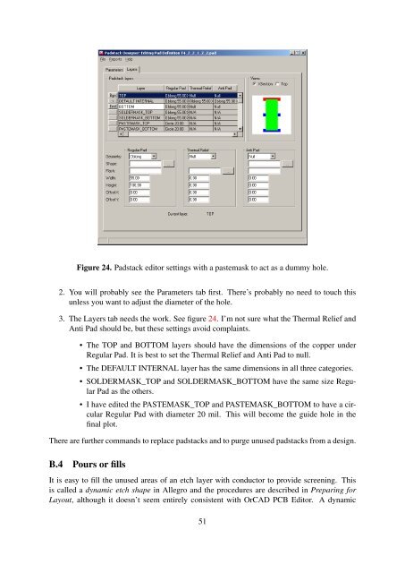
Figure 24. Padstack editor settings with a pastemask to act as a dummy hole.<br />
2. You will probably see the Parameters tab first. There’s probably no need to touch this<br />
unless you want to adjust the diameter of the hole.<br />
3. The Layers tab needs the work. See figure 24. I’m not sure what the Thermal Relief and<br />
Anti Pad should be, but these settings avoid complaints.<br />
• The TOP and BOTTOM layers should have the dimensions of the copper under<br />
Regular Pad. It is best to set the Thermal Relief and Anti Pad to null.<br />
• The DEFAULT INTERNAL layer has the same dimensions in all three categories.<br />
• SOLDERMASK_TOP and SOLDERMASK_BOTTOM have the same size Regular<br />
Pad as the others.<br />
• I have edited the PASTEMASK_TOP and PASTEMASK_BOTTOM to have a circular<br />
Regular Pad with diameter 20 mil. This will become the guide hole in the<br />
final plot.<br />
There are further commands to replace padstacks and to purge unused padstacks from a design.<br />
B.4 Pours or fills<br />
It is easy to fill the unused areas of an etch layer with conductor to provide screening. This<br />
is called a dynamic etch shape in Allegro and the procedures are described in Preparing for<br />
Layout, although it doesn’t seem entirely consistent with <strong>OrCAD</strong> <strong>PCB</strong> Editor. A dynamic<br />
51