Cadence OrCAD PCB Designer
Cadence OrCAD PCB Designer
Cadence OrCAD PCB Designer

Create successful ePaper yourself
Turn your PDF publications into a flip-book with our unique Google optimized e-Paper software.
Electronic Design Project 2<br />
<strong>Cadence</strong> <strong>OrCAD</strong> <strong>PCB</strong> <strong>Designer</strong><br />
Notes for demonstrators<br />
Professor John H. Davies ∗<br />
October 28, 2008<br />
Objectives<br />
After completing these laboratories, you should be able to:<br />
• capture, simulate and lay out a simple, one-transistor amplifier on a one-sided printed<br />
circuit board (<strong>PCB</strong>) with manual routing<br />
• lay out an instrumentation amplifier based on three op-amps, comparing one-sided<br />
and double-sided boards with automatic routing<br />
• lay out a mixed-signal system, comparable with the final project in this course, with<br />
precautions to prevent interference between the analog and digital sections.<br />
Preamble<br />
You must bring a bound, A4 notebook to every laboratory for recording your results. It<br />
needn’t be a new book for this course or anything fancy but you will get no marks if you<br />
don’t have a book with you. Please don’t use the same book for another course this year.<br />
You must also have university (Novell) printer credits so that you can print the circuits,<br />
layouts and the results of your simulations. These should be attached firmly into your<br />
laboratory book for future reference.<br />
The first part of these laboratories, which is a ‘pencil and paper’ analysis of a onetransistor<br />
amplifier, must be written up in your laboratory book as you do it. The remaining<br />
parts do not need much of a record to be kept but you will find it useful to make a note of<br />
tricks and tips for using <strong>OrCAD</strong>. This will be valuable when you have to design your own<br />
circuits in Team Design Project 3 next year and in subsequent projects.<br />
These laboratories form part of your professional development because it is expected<br />
that every electronic engineer should be able to design, populate and test a printed circuit<br />
board (<strong>PCB</strong>). You are therefore required to complete all tasks to be awarded credit. Most<br />
of the marks are awarded simply for completion but extra marks will be awarded for good<br />
layouts.<br />
Note for direct entrants: I’ve tried to make connections with material covered last year,<br />
which you may find utterly unhelpful! Please ask me if you are missing any background<br />
knowledge.<br />
∗ Email: jdavies@elec.gla.ac.uk<br />
1
Contents<br />
1 Introduction 2<br />
2 One-transistor amplifier: simple analysis 4<br />
3 Schematic capture and simulation 6<br />
4 Preparation for <strong>PCB</strong> layout 10<br />
5 <strong>OrCAD</strong> <strong>PCB</strong> Editor 18<br />
6 Instrumentation amplifier – single-sided board 27<br />
7 Instrumentation amplifier – double-sided board 37<br />
8 A mixed-signal system 40<br />
9 Summary: <strong>PCB</strong> design flow 45<br />
10 How to correct a layout if you spot an error in the circuit 46<br />
A Where to learn more 47<br />
B Power-user tips and random jottings 49<br />
1 Introduction<br />
This series of exercises introduces you to schematic capture, simulation and <strong>PCB</strong> layout using<br />
the <strong>Cadence</strong> <strong>OrCAD</strong> design suite. This comprises three main applications:<br />
• Capture for the schematic capture of circuits, which enables a circuit to be rapidly drawn<br />
on the screen. It offers great flexibility compared with a traditional pencil and paper<br />
drawing, as design changes can be incorporated and errors corrected quickly and easily.<br />
(On the other hand, it is much faster to develop the outline of a circuit using pencil and<br />
paper.) A netlist, which describes the components and their interconnections, is the link<br />
to PSpice and <strong>PCB</strong> Editor.<br />
• PSpice to simulate a captured circuit and confirm that it performs as specified. Plots<br />
were produced by a separate application called Probe in the past and I’ll stick to this<br />
name, although it has long been integrated into PSpice.<br />
• <strong>PCB</strong> Editor (Allegro) for the layout of printed circuit boards. This includes an automatic<br />
router (SPECCTRA) that works out the arrangement of tracks needed to connect your<br />
components on the <strong>PCB</strong>. The output is a set of files that can be sent to a manufacturer or<br />
the electronics workshop in the Rankine Building.<br />
2
The first two should be familiar from last year but the third is new. These programs are accessed<br />
via networked Windows PCs in the department, with up to 40 users at any one time. Unfortunately<br />
the licensing arrangements do not permit access from outwith the Rankine Building. A<br />
demonstration version is available; please ask.<br />
We are using <strong>PCB</strong> <strong>Designer</strong> for the first time this year because our previous application,<br />
Layout, is being discontinued. <strong>OrCAD</strong> <strong>PCB</strong> <strong>Designer</strong> is the most basic version of <strong>Cadence</strong>’s<br />
Allegro suite for <strong>PCB</strong> design and much of the documentation refers to ‘Allegro’ rather than<br />
‘<strong>PCB</strong> Editor’. Allegro is widely used in industry and is similar to the <strong>Cadence</strong> software for<br />
laying out integrated circuits (ICs), which you will experience in Digital Circuit Design 3.<br />
That’s the good news: Allegro is far more powerful than we need for laying out our simple<br />
circuits and the vast number of features can seem bewildering. It is also new to your instructors<br />
and this course will be a learning experience for all of us!<br />
Fixup. I have encountered numerous problems with the software, mainly due to incompatibilities<br />
between the libraries supplied for Capture and those for <strong>PCB</strong> Editor. These are marked<br />
as Fixups. I expect that we will find smoother ways around these difficulties in the future but<br />
you are the guinea-pigs. I’d also be grateful for suggestions for improving these instructions.<br />
There is extensive online help for all these programs although I have to admit that it could be<br />
better organised. Please try this before asking a demonstrator for help – it is part of the learning<br />
process. Most ‘professional’ software is so complicated that even experts make regular use of<br />
the help files.<br />
Three types of information are needed for each component and are stored in libraries.<br />
• Electrical symbols are used to draw the circuit in Capture.<br />
• Electrical models allow you to simulate the circuit in PSpice.<br />
• Footprints show the size and shapes of the pads (where the pins are soldered to the<br />
board) and the outline of the package. They are used to lay out the circuit in <strong>PCB</strong> Editor.<br />
The first two should again be familiar from last year. Remember that each type of component<br />
is kept in a different library file and you must select the files needed for a particular design. The<br />
third piece of information is new. You might wonder why yet another library is needed. The<br />
reason is that components with the same electrical behaviour come in different packages. For<br />
example, an integrated circuit might come in two versions:<br />
• a traditional, plastic dual-in-line package (PDIP) with pins 0.1 ′′ apart<br />
• a smaller, surface-mount device (SMD) with pins only 0.5 mm apart, if it has pins at all<br />
The opposite is also true: resistors of a particular shape come in a wide range of values. Further<br />
information is needed to describe the characteristics of the printed circuit board on which the<br />
components are mounted.<br />
Each circuit design is regarded as a project and a project manager groups all the files together<br />
in a subdirectory. These files should be stored in your work space on the University’s<br />
central system, accessed via the network as the H drive. Do not store files in any other place on<br />
the network or on a computer – they will be erased.<br />
The <strong>Cadence</strong> system provides many facilities which are not needed for these introductory<br />
designs. Please do not attempt to use commands which are not described in these instructions;<br />
3
Figure 1. A simple, one-transistor amplifier that can be simulated using Spice.<br />
you will waste a lot of time and may lose large portions of your work. Please ask for help when<br />
you encounter problems – you are likely to make matters worse if you try to fix things yourself.<br />
You should know this by now, but a reminder is never a bad idea: Save your work frequently<br />
and take regular backups of important circuits.<br />
2 One-transistor amplifier: simple analysis<br />
Figure 1 shows the circuit of a simple amplifier with one transistor. It is intended to amplify<br />
audio signals, say from 20 Hz – 20 kHz. I have used international standard symbols for the<br />
components, such as the zigzag line for a resistor rather than the anonymous rectangle preferred<br />
by the IET.<br />
An engineer always makes a rough design using pencil and paper before simulating it. You<br />
will not learn how to design this particular circuit until the Analogue Electronics 2 course later<br />
in year, so we shall ‘reverse engineer’ it instead. The calculations are simple and should be<br />
done in your laboratory book. You should be pleasantly surprised to find that you don’t need to<br />
know much about transistors to analyse this. In fact you did most of it in Electronic Engineering<br />
1Y. Make sure that you recognise the emitter, base and collector.<br />
We first find the bias point, operating point or quiescent point. This means the conditions<br />
when no signal is applied and the circuit is ‘resting’. There is no input and you can therefore<br />
ignore the 10 mVac source.<br />
1. Resistors R 1<br />
and R 2<br />
form a simple potential divider if we ignore the other components<br />
attached to them. (We should go back and check this assumption when the currents are<br />
known.) Calculate the voltage on the base of the transistor Q 1<br />
.<br />
Hint for demonstrators.<br />
2.7 V ❦<br />
4
2. The base–emitter junction of a transistor is a forward-biassed diode (hence the arrow on<br />
its symbol) and therefore has a voltage of V be<br />
≈ 0.7V across it. Calculate the voltage on<br />
the emitter.<br />
Hint for demonstrators.<br />
2.0 V ❦<br />
3. We now know the voltage across the resistor R 4<br />
. Calculate the current through it.<br />
Hint for demonstrators.<br />
11.1 mA (the aim was 10 mA) ❦<br />
4. The current into the base of a transistor is much smaller than the other two currents, so<br />
the current flowing into the collector is nearly equal to that flowing out of the emitter.<br />
Calculate the voltage dropped across R 3<br />
and hence the voltage on the collector.<br />
Hint for demonstrators.<br />
4.3 V across R 3<br />
so V c = 5.7V (the aim was 6 V) ❦<br />
This has shown why the four resistors are needed but not the capacitors. What is the expression<br />
for the impedance of a capacitor (remember that it is complex), and how does its magnitude<br />
depend on frequency? The function of the capacitors in this circuit is to allow high frequencies<br />
to pass – the signals that we wish to amplify – but to block the steady voltages that set the bias<br />
point.<br />
• We have seen that the base of the transistor is kept at a particular voltage by the potential<br />
divider, which sets the bias point. The capacitor C 1<br />
on the input isolates this voltage from<br />
the previous stage of the system but lets the signal through.<br />
• Look at the circuit through which the input signal flows. It passes ‘through’ the capacitor<br />
C 1<br />
, through the base–emitter junction of the transistor, through R 4<br />
and C 2<br />
in parallel, and<br />
back to the ground connection of the input. This shows that R 4<br />
is in series with the input<br />
and will reduce its magnitude. We really want all the voltage to be applied across the<br />
base–emitter junction, where it will be amplified by the transistor. However, we can’t<br />
simply get rid of R 4<br />
because it is needed to set the bias point – it determines the current<br />
through the transistor, as you saw above. The solution is to put the bypass capacitor C 2<br />
across the resistor.<br />
The bias has zero frequency so it all flows through the resistor. The signal has a ‘high’ frequency<br />
so most of it flows through the capacitor, which should have a much smaller impedance than<br />
the resistor. Ideally the impedance of C 2<br />
should obey |Z C<br />
( f )| ≪ R 4<br />
for all frequencies in the<br />
signal. Is this true for the values in figure 1?<br />
Hint for demonstrators. No! At the lowest frequency of 10 Hz, X C<br />
= 1/2π fC = 160kΩ,<br />
which is much larger than R 4<br />
= 180Ω. The capacitor should be a thousand times larger. This<br />
will be shown by the simulation. ❦<br />
Finally, we would like to estimate the voltage gain of the circuit. This needs some background<br />
on transistors that you have not yet covered so I’ll just quote the result. The gain is<br />
given by<br />
V out<br />
= −g m R<br />
V 3<br />
(1)<br />
in<br />
5
where g m is called the transconductance of the transistor, defined by ∂I c /∂V be<br />
. Its value is<br />
given by<br />
g m = I c<br />
V T<br />
(2)<br />
where I c is the collector current at the bias point, which you have calculated already, and V T<br />
is called the thermal voltage. This is in turn given by V T<br />
= k B<br />
T /e where k B<br />
is Boltzmann’s<br />
constant (remember this from physics courses?), T is the absolute temperature and e is the magnitude<br />
of the electronic charge. Don’t worry about the formula because the value of V T<br />
is close<br />
to 25 mV at room temperature, which isn’t too hard to remember. Now you can calculate the<br />
transconductance and voltage gain. What is the gain in decibels (dB)? – you should remember<br />
the definition.<br />
Hint for demonstrators. Transconductance g m = 11mA/25mV = 0.44S, giving a gain of<br />
−0.44 × 390 = −170.<br />
The gain in decibels is defined as<br />
∣ ∣∣∣ output voltage<br />
20log 10<br />
input voltage ∣ = 45dB. (3)<br />
❦<br />
☛ Milestone: Show your results to a member of staff and be prepared to explain them.<br />
An interesting feature is that we haven’t used any details of the transistor at all! This makes<br />
it easy to design circuits based on bipolar junction transistors, to give them their full name.<br />
Now we’ll capture the circuit in <strong>OrCAD</strong>, simulate it and see how good these estimates are.<br />
3 Schematic capture and simulation<br />
Always create a fresh directory for every new project in <strong>OrCAD</strong>. You get all manner of strange<br />
errors if you do not do this, from which it seems impossible to recover. In any case it helps to<br />
keep your work organised.<br />
Select Start > Programs > <strong>OrCAD</strong> 16.0 > <strong>OrCAD</strong> Capture (the version number may be<br />
higher if <strong>OrCAD</strong> has been upgraded). I use ‘>’ throughout this document to show the levels of<br />
a hierarchical menu. There will be a short delay while the software is loaded and the licence<br />
server is accessed. Wait until the red splash screen disappears. The screen will then show the<br />
<strong>OrCAD</strong> Capture main window with a menu bar and a tool bar. A sub-window shows the session<br />
log, which may be minimised.<br />
3.1 Create a project<br />
I’ll repeat this: Your first action must always be to create a new directory to hold all the files<br />
for a new project. Next, create an <strong>OrCAD</strong> project.<br />
1. Select File > New > Project from the menu bar.<br />
2. In the New Project dialog box:<br />
6
• Select an Analog or Mixed A/D project. This choice is essential or you will not be<br />
able to simulate the circuit.<br />
• Give the project a meaningful name.<br />
• Click on the Browse key, select your H drive and navigate to a suitable location.<br />
Click the Create Directory button if you haven’t already made a new directory for<br />
the design and enter a suitable name. Click OK.<br />
• Select this new directory and click OK. The path and directory now show in the<br />
location box (if you can see them – they are usually too long). Click on OK in the<br />
New Project dialog box.<br />
• Click Next.<br />
3. Select the Create a blank project button in the small dialog box that appears and click<br />
OK.<br />
4. Your project will now be created. The Project Manager window (headed name.opj)<br />
shows the files associated with your design and the resources that will be used, such<br />
as library files. Check that the File tab is selected if the view looks unfamiliar.<br />
5. Open the window SCHEMATIC1: PAGE1 for your design. There is a Title box in the<br />
lower right-hand corner. Double-click on the placeholders, which are in angle brackets<br />
, and replace them with a descriptive title and so on.<br />
3.2 Draw the circuit<br />
Lay out the circuit in figure 1 on page 4. The method is exactly the same as last year, but here<br />
are a few tips in case you have forgotten. The names of the components are listed in table 1<br />
on page 12. The capacitor C 2<br />
is an electrolytic type, which must be installed with the correct<br />
polarity or it will explode. Its parameter CMAX is the maximum working voltage, which is not<br />
needed for simulation. I’ve renamed some of the components to make their functions clearer.<br />
• All circuits must have a ground node called 0 (zero) for simulation. You will get confusing<br />
messages about unconnected nodes if you forget this. Get it from the ground button<br />
on the right.<br />
• PSpice is unhelpful about notation. Usage like 10ˆ6 doesn’t work but it won’t tell you!<br />
(It will just stop at the caret and take the value as 10.) Use 1e6 or 1Meg instead – not 1M<br />
because a single m or M means milli, not mega.<br />
• Libraries must be chosen from the pspice folder, otherwise the components will not have<br />
PSpice models and you will not be able to simulate them.<br />
• Simple components like resistors are in the analog library, sources such as VDC are<br />
in source and the param block is in special. Use Search if you can’t guess where a<br />
component is located. You will probably need to do this for the transistor.<br />
• Always join components with wires, not by placing them so close that their pins overlap.<br />
This can cause strange errors.<br />
7
• Wires and components sometimes become joined incorrectly if you move them about.<br />
Use Place > Junction or the junction tool from the buttons on the right to eliminate<br />
spurious connections.<br />
• Place voltage probes on the points on the circuit where you want to plot the values. This<br />
is easier than selecting them from the list of variables in Probe.<br />
• I like to use off-page connectors to label nodes such as input and output, where the<br />
voltages will be plotted. There is a menu and button for these. The names appear in<br />
Probe, which makes it much easier to identify the traces.<br />
3.3 Simulate the circuit<br />
Set up a Simulation Profile to make an AC Sweep of the circuit from 10 Hz to 100 kHz. Remember<br />
that the sweep should be logarithmic in decades, not linear. About 10 points per decade<br />
should be adequate. Run the simulation and plot the results. Plot the voltage gain in decibels<br />
(dB) rather than the output voltage itself. You should remember how to do this from the RC<br />
filter last year but here is a reminder.<br />
1. Delete all the traces in the plot window.<br />
2. Choose Trace > Add Trace from the menu bar. The dialog box shows variables on the<br />
left and functions on the right.<br />
3. Choose the DB function from the right, and inset the output voltage divided by the<br />
input voltage using the variables from the left. The final expression should look like<br />
DB(V(Output)/V(Input)) if you used the same names as me.<br />
Hint for demonstrators. If the PSpice menu and toolbar are missing, the student has probably<br />
forgotten to choose ‘Analog or Mixed A/D’ when the project was created. Copy and paste<br />
the circuit into a new project with the correct type.<br />
Many students will have forgotten what is meant by voltage gain: output voltage divided<br />
by input voltage. I have explained how to use the decibel function in probe but there are more<br />
advanced approaches to request this type of plot directly from the menus in Capture, using<br />
PSpice > Markers > Plot Window Templates. . . and choosing Bode Plot - dB or Voltage Gain.<br />
The input must be 1 Vac for this.<br />
My results are in figure 2. The gain never reaches its target value. The wide plateau around<br />
1 kHz is where the gain is limited by R 4<br />
because the bypass capacitor is too small. ❦<br />
• Does the gain match the estimated value? Is it reasonably constant with frequency across<br />
the audio range?<br />
• You should also check that the bias point agrees with the pencil-and-paper calculations.<br />
Go back to Capture and click the V button to get the voltages on all nodes. Check the<br />
current through the transistor too.<br />
I found that the gain did not behave as expected (so now I have given you the answer to the first<br />
question!) and suspect that the capacitor C 2<br />
across the emitter resistor R 4<br />
is too small. Check<br />
8
Figure 2. Gain as a function of frequency.<br />
this by simulating the circuit for a set of values of C 2<br />
. This requires a parameter. You should<br />
remember how to do this from Electronic Engineering 1X and 1Y but it is clumsy so here is a<br />
reminder.<br />
1. First place a param block from the special library.<br />
2. Open its spreadsheet by double clicking or with the Edit Properties. . . contextual menu<br />
item.<br />
3. Choose Add row. . . (or column, depending on the orientation of your spreadsheet) to<br />
create the parameter. Give it a name, such as Cap2, and a default value (use its previous,<br />
fixed value). Click OK to get rid of the dialog box.<br />
4. The parameter does not appear on the schematic by default so you must select the newly<br />
added row/column in the spreadsheet, click the Display button, select Name and Value<br />
and finally click OK.<br />
5. Change the value of C 2<br />
from a fixed value to the parameter. Remember that the parameter<br />
must be enclosed in curly brackets {} in the Value field.<br />
6. Create a new simulation profile with the same frequency sweep plus a parametric sweep<br />
on Cap2 from 0.1 µF – 1000 µF. Use a logarithmic sweep with one value per decade. Run<br />
the simulation and print your results in colour. The printout looks better if you make the<br />
lines thicker. (If you print in black and white, set the number of trace colours to zero so<br />
that the curves show up.)<br />
Does a larger value of C 2<br />
improve the performance? What value would you recommend?<br />
☛ Milestone:<br />
Show your results to a member of staff and be prepared to explain them.<br />
9
Figure 3. Gain as a function of frequency for different bypass capacitors.<br />
Hint for demonstrators. My results are in figure 3. Increasing the bypass capacitor improves<br />
the gain until it is limited at low frequency by C 1<br />
instead. There isn’t much difference between<br />
the results for 100 µF and 1000 µF so I would use 100 µF. ❦<br />
4 Preparation for <strong>PCB</strong> layout<br />
Once the design of the circuit has been finalised, it should be laid out on the printed circuit<br />
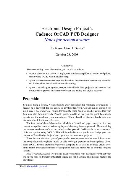
board (<strong>PCB</strong>). This takes a few steps before you leave Capture. The overall design flow for<br />
making a <strong>PCB</strong> is shown in figure 4 on the next page and there is a summary in section 9.<br />
4.1 Edit the circuit<br />
First, the ‘virtual components’ in the schematic must be replaced by real components. Here<br />
this means the voltage sources and param block. There is no way that you can build a real<br />
circuit with a param block for instance! (Well, you could use a pair of sockets and unplug the<br />
component to change it.) The real circuit has connectors for input, output and power, which<br />
must be placed instead. This is shown in figure 5. The types of connector are HEADER 2 and<br />
the like. They are in the connector library, which is in the directory one level above pspice.<br />
The connectors are oriented so that pin 1 is connected to ground in both cases. It is shown by a<br />
square marker on the <strong>PCB</strong>. I have changed the names to make them more descriptive than the<br />
defaults, such as HEADER 2; do not edit the references J1 and J2. Add text to label the pins<br />
of each connector and put your name on the circuit, or you won’t be able to identify it when it<br />
comes out of the printer.<br />
Hint for demonstrators. Some students change the Reference (J1 or J2) of the connectors<br />
to Input or Output instead of changing the Value (HEADER 2 or HEADER 3). This causes<br />
trouble with the netlister later on. ❦<br />
10
Capture<br />
Draw<br />
schematic<br />
<strong>PCB</strong> Editor<br />
Set up bare board<br />
(outline, design rules)<br />
Add<br />
footprints<br />
Create<br />
netlist<br />
Engineering<br />
Change Order<br />
(ECO)<br />
Libraries<br />
Place and arrange<br />
components<br />
Export to<br />
SPECCTRA<br />
Route board<br />
manually<br />
Route board<br />
automatically<br />
Check vias,<br />
gloss board<br />
Route board<br />
automatically<br />
Spread and<br />
mitre tracks<br />
Annotate and print<br />
board<br />
Return to<br />
<strong>PCB</strong> Editor<br />
Figure 4. Design flow for making a <strong>PCB</strong> with Capture and <strong>PCB</strong> Editor. The three paths for<br />
<strong>PCB</strong> Editor depend on whether the tracks are drawn manually (as we shall do for our first<br />
design), automatically within <strong>PCB</strong> Editor, or by running the automatic router (SPECCTRA) as<br />
a separate application.<br />
Input<br />
Gnd<br />
J1<br />
2<br />
1<br />
C1<br />
1u<br />
R1<br />
7.4k<br />
Q1<br />
R3<br />
390<br />
BFY51<br />
3<br />
2<br />
1<br />
J2<br />
Output<br />
+10V<br />
Output<br />
Gnd<br />
Input<br />
R2<br />
2.7k<br />
R4<br />
180<br />
C2<br />
100u<br />
16V<br />
Figure 5. The simple, one-transistor amplifier with only real components, ready for layout.<br />
11
Table 1. Footprints of components for the one transistor amplifier.<br />
Part Name Footprint<br />
Resistor R RC400<br />
Capacitor C RC500<br />
C, polarised C_elect RC200_RADIAL<br />
Connector HEADER 2 MOLEX2<br />
Connector HEADER 3 MOLEX3<br />
Transistor BFY51 TO5 (letter ‘oh’ not number zero)<br />
Fixup. There is a stupid incompatibility between the electrolytic capacitor C_elect in the<br />
analog library and the footprints. The pins of the footprints are numbered 1, 2 but those of the<br />
capacitor are p, n. This means that the software cannot match the capacitor to its footprint. Edit<br />
the electrolytic capacitor and change the numbers of its pins to resolve this. You will need to<br />
edit parts in future so it is useful to learn the procedure.<br />
1. Select the electrolytic capacitor and choose Edit > Part from the menu bar. A window<br />
will open with an enlarged view of the capacitor.<br />
2. The negative pin is shown as a red line on the right. Select it and and choose Edit ><br />
Properties. . . . This brings up the Pin Properties dialogue box.<br />
3. Change the Number to 2 and click OK. Don’t worry about the name.<br />
4. The positive pin is shown as a circle. Select this and edit its Number to 1.<br />
5. Choose File > Close (or click the close box as usual). You have the choice of updating<br />
this part alone, or all ‘part instances’ – that means all C_elect components in your design.<br />
Of course there is only one so it doesn’t matter whether you choose Update Current or<br />
Update All in this case.<br />
Print the drawing sheet and stick it into your laboratory book. The circuit takes up only a small<br />
part of the page, so it is a good idea to choose File > Print Area > Set and mark out a rectangle<br />
that includes only the part of the page that you wish to print.<br />
☛ Milestone:<br />
Have your drawing checked before you go any further.<br />
4.2 Add footprints<br />
We must next associate footprints with the components so that the <strong>PCB</strong> can be laid out. These<br />
are the physical outlines of the components including the positions of the pins. The pspice<br />
library contains footprints already but unfortunately they are mostly wrong. We must therefore<br />
enter the correct footprints now. The footprints for this circuit are listed in table 1. Please type<br />
carefully and don’t muddle the letter O with the numeral 0.<br />
1. Drag the cursor in Capture so that all the components are enclosed in a rectangle. Do not<br />
include the title box.<br />
12
2. Choose Edit > Properties. . . from the menu bar, which brings up the Properties spreadsheet.<br />
3. Type each name into the <strong>PCB</strong> Footprint field of the Properties spreadsheet in Capture.<br />
All the resistors have same footprint so use copy and paste for speed.<br />
A problem with footprints. . .<br />
<strong>PCB</strong> Editor comes with a small library of footprints but they are intended for commercial production<br />
and are unsuitable for boards made in this department. Many components are missing<br />
too. Mr I. Young of the SPEED group in this department has therefore designed a more suitable<br />
set of footprints. There is a catalogue at the end of this handout, which you should be able to<br />
match with the components kept in stores.<br />
4.3 Design rules check<br />
The next step is a Design Rules Check, to ensure that there are no errors.<br />
1. Click on the Project Manager window and highlight your design (with extension .dsn).<br />
2. Select Tools > Design Rules Check. . . from the menu bar.<br />
3. Choose options (probably the default):<br />
• report identical part references<br />
• check unconnected nets<br />
4. Click OK, and look at the report in the Session log window. There is no positive message<br />
that all rules have been passed successfully, just an absence of complaints. The final line<br />
is usually Check bus width mismatch; I don’t know why it starts with Check, which is<br />
misleading, rather than Checking like the others.<br />
5. Return to your drawing and correct any errors. These may be shown by green circles<br />
(a strange choice of colour for an error!). Repeat the Design Rules Check until it runs<br />
silently.<br />
6. You may wish to run the Design Rules Check and select Action > Delete existing DRC<br />
markers to get rid of the green circles. They do not vanish by themselves.<br />
4.4 Make a bare board in <strong>PCB</strong> Editor<br />
The simplest way of creating a <strong>PCB</strong> is first to set up an empty <strong>PCB</strong>, then to add your components<br />
and connections to the board. This follows the design flow shown in figure 4 on page 11.<br />
First create a directory allegro within your directory for the current project. <strong>PCB</strong> Editor<br />
likes to keep its files in a directory with this name. Then choose Start > Programs > <strong>OrCAD</strong><br />
16.0 > <strong>OrCAD</strong> <strong>PCB</strong> Editor, which opens the <strong>OrCAD</strong> <strong>PCB</strong> <strong>Designer</strong> application (<strong>Cadence</strong> seem<br />
muddled about the name). I’ll leave the details of the interface until later because we need only<br />
two dialogue boxes for this step.<br />
13
Set up the search paths for footprints<br />
I mentioned above that we use a local library for footprints rather than those supplied with<br />
Allegro. We must therefore tell <strong>PCB</strong> Editor to look in the local library first. You should<br />
only have to do this once (and maybe not at all, depending on how the software and PCs are<br />
configured).<br />
1. Choose Setup > User Preferences. . . from the menu bar, which brings up the User<br />
Preferences Editor.<br />
2. Choose Design_paths in the list of Categories.<br />
3. We first need to change psmpath, which is where <strong>PCB</strong> Editor looks for library symbols.<br />
Click on the Value button (which shows only ‘. . . ’). This brings up a box entitled<br />
psmpath Items.<br />
4. Click the New (Insert) button (the leftmost one), which adds an empty item to the list<br />
with another ‘. . . ’ button. Click this button, which brings up the usual Windows Select<br />
Directory box.<br />
5. Navigate to the Elecapps drive (Q), find the allegro directory, then pcb_lib and finally<br />
symbols. Click OK to select this directory.<br />
6. Next we must tell <strong>PCB</strong> Editor to look in our local directory before the default libraries,<br />
denoted by $psmpath. Click on $psmpath followed by the Move Down arrow. The<br />
psmpath Items box should now look like figure 6 on the next page except that your<br />
directories are different (my computer is not on the same network). Click OK.<br />
7. Follow the same procedure for padpath, which uses the padstacks directory in pcb_lib.<br />
This is the information for the padstacks, the copper islands used for mounting components,<br />
including holes for pin-through-hole components.<br />
8. Click OK to dismiss the User Preferences Editor.<br />
You should never have to do this again!<br />
Define the board<br />
Choose File > New. . . from the menu. In the first dialogue box, set the Drawing Type to Board<br />
(wizard). Click Browse. . . , navigate to your new allegro directory and give the board a name<br />
such as bare.brd. Click Open then OK to bring up the new board wizard. This takes you<br />
through several screens to define the parameters of the <strong>PCB</strong>. Some of these are obvious, such<br />
as the size of the board, while others set up the design rules – the width of tracks on the <strong>PCB</strong>,<br />
how much space must be left between them, and so on.<br />
1. The first screen is purely descriptive. Read it, then click Next >.<br />
2. This asks for a board template. We don’t have one so select No (probably the default)<br />
and click Next >.<br />
14
Figure 6. Completed dialogue box for setting up psmpath. Your directory path will be different.<br />
3. You are next asked for a ‘tech’ file. This is short for a technology file, which specifies the<br />
design rules – number of layers, widths and separation of tracks and so on. We won’t use<br />
one for this design so select No and click Next >.<br />
4. This asks for a board symbol. We don’t have one so select No again and click Next >.<br />
5. We now reach the screens for the parameters that must be set up. The units should<br />
be Mils. These are not millimeters but the American term for thousandths of an inch;<br />
1mm ≈ 40mils. All dimensions are given in these units so get used to them.<br />
Leave the drawing size at A. This is an American size but you aren’t allowed European<br />
A4 if the units are mils. Leave the origin at the centre.<br />
6. Set the grid spacing to be 25 mils.<br />
The Etch layer count is the number of copper layers on the board – the number of layers<br />
of tracks for signals and power. Leave this at 2, although we shall use only one layer in<br />
the first design.<br />
Don’t worry about the artwork films – we don’t use them.<br />
7. Leave the names of the layers as Top and Bottom and their types as Routing Layer.<br />
8. Enter 30 for the Minimum Line width (in mils). This value will propagate into the other<br />
boxes. It means 0.03 ′′ or about 0.76 mm, which is very wide for a track nowadays but<br />
makes the board easy to lay out.<br />
For the Default via padstack, click on the button with . . . and choose Via80. This first<br />
design is far too simple to need vias, which carry a signal from one layer of the <strong>PCB</strong> to<br />
another, but they may be required later.<br />
9. Rectangular board (it’s curious that a circular board is the default).<br />
15
10. Enter a width of 3000 and height of 2000 mils. This defines the board outline as 3 ′′ × 2 ′′ .<br />
There is no corner cutoff.<br />
Specify the Route keepin distance as 100. A keepin means that objects must be kept<br />
inside the specified region. In this case it means that tracks cannot go any closer than<br />
100 mils to the edge of the board. It gives a border around the <strong>PCB</strong> to aid handling and<br />
manufacture. (We’ll encounter keepouts as well later.)<br />
Set the Package keepin distance to 250. Components must be placed within this keepin<br />
and therefore cannot be closer than 250 mils to the edge of the board. The gap between<br />
the two keepins allows you to run tracks around the outside of all the components, which<br />
is often helpful on a more complicated board.<br />
11. Click Finish – that’s it.<br />
This has set up the design rules and made an empty board which you can see in the main<br />
window of <strong>PCB</strong> Editor, shown in figure 8 on page 19. There are three rectangles for the board<br />
outline, route keepin and package keepin. Choose File > Save and close <strong>PCB</strong> Editor.<br />
Hint for demonstrators. If students can’t find Via80, it means that <strong>PCB</strong> Editor can’t find our<br />
local library. Check that the paths have been set up correctly. ❦<br />
The next step is to return to Capture and send the circuit to <strong>PCB</strong> Editor so that it can be<br />
added to the bare board.<br />
4.5 Create a netlist<br />
The information about your design is sent from Capture to <strong>PCB</strong> Editor in the form of a netlist,<br />
which contains a description of the circuit and its components. (There are actually three files<br />
but you don’t need to look at them.)<br />
1. Highlight your design in the Project Manager window of Capture.<br />
2. Select Tools > Create Netlist. . . from the menu bar, which brings up a dialogue box as in<br />
figure 7 on the next page. Make sure that the <strong>PCB</strong> Editor tab is active.<br />
3. Check that the <strong>PCB</strong> Footprint box contains <strong>PCB</strong> Footprint.<br />
4. Check that the box underneath for Create <strong>PCB</strong> Editor Netlist is selected.<br />
5. Under Options, the Netlist Files Directory should be shown as allegro. Select Create or<br />
Update <strong>PCB</strong> Editor Board (Netrev).<br />
6. For Input Board File, choose the bare board that you have just set up. Click on the ‘. . . ’<br />
button to navigate.<br />
7. The Output Board File should show something sensible automatically; edit it if not. It<br />
should use the new allegro directory.<br />
8. Under Board Launching Option, select Open Board in <strong>OrCAD</strong> <strong>PCB</strong> Editor. This is required<br />
because our licence doesn’t cover the full version of Allegro.<br />
16
Figure 7. Completed dialogue box for netlisting the design and sending it to <strong>PCB</strong> Editor. Your<br />
file names will be different.<br />
9. The entries in the dialogue box should now resemble figure 7 except that your pathnames<br />
are different. Click OK to dismiss this dialog box and start the netlister.<br />
You will be warned that your design will be saved by Capture, then a Progress box will appear<br />
to show the various processes needed: Netlisting the design followed by Updating <strong>OrCAD</strong> <strong>PCB</strong><br />
Editor Board. <strong>PCB</strong> Editor will then be launched with your new board.<br />
• You will probably see a Warning box, which tells you that Netrev succeeded with warnings.<br />
Check the Session Log if this happens. Messages about RVMAX and CMAX can be<br />
ignored; these are maximum voltage ratings of the components and are not important for<br />
this circuit. Pay attention to any others and seek advice.<br />
• <strong>OrCAD</strong> <strong>PCB</strong> Editor will also give you a warning that Database was last saved by a<br />
higher tier tool, which you can ignore.<br />
• Consult a demonstrator if you get an error and the process fails.<br />
You should now see your empty board outline on the screen of <strong>PCB</strong> Editor again; the components<br />
are invisible at this stage. Close Capture and allow it to save all the files.<br />
17
Hint for demonstrators. If <strong>PCB</strong> Editor complains that no product licences are available,<br />
the student has probably forgotten to select Open Board in <strong>OrCAD</strong> <strong>PCB</strong> Editor. A different<br />
message appears if we run out of licences, which I hope will not happen.<br />
If the Netlist Files Directory does not show as allegro automatically, and nothing appears to<br />
happen when you run the netlister, there is a problem with the permissions. Netlisting must be<br />
performed once on each computer by a user with administrator privileges before it will work<br />
for anybody else. Don’t ask me why. . .<br />
<strong>PCB</strong> Editor is almost always launched even if there was a fatal error during netlisting, which<br />
misleads students into thinking that the process was successful. It is vital to check the session<br />
log. ❦<br />
5 <strong>OrCAD</strong> <strong>PCB</strong> Editor<br />
<strong>OrCAD</strong> <strong>PCB</strong> Editor is the basic version of the Allegro <strong>PCB</strong> Editor from <strong>Cadence</strong>. Despite<br />
being ‘basic’ it is vastly more powerful than is needed for the simple designs that we shall<br />
lay out in this course. Its interface will probably feel unfamiliar because the application was<br />
originally developed for unix and has been ported to Windows with minimal changes. Some<br />
distinctive features will become obvious almost immediately.<br />
• The main window, which shows your design, has no scroll bars.<br />
• There is always one design open; you cannot open more than one, nor close the current<br />
design without opening a new one or exiting the application.<br />
• There is no ‘null’ tool, such as the pointer shown by most drawing applications when no<br />
other tool is selected. If you are not sure which tool is active, right-click in a region of<br />
empty space and choose Done from the contextual menu to deselect the current tool.<br />
5.1 The screen<br />
<strong>PCB</strong> Editor needs a big screen – the elderly laptop that I have used while writing these instructions<br />
is not large enough to show all the toolbars! These are the main elements of the<br />
application, shown in figure 8 on the next page.<br />
• Menu bar along the top as usual.<br />
• Toolbars in two rows under the menu bar and a further column down the left-hand side.<br />
Their arrangement depends on the size of the screen. Hover the pointer over a button to<br />
reveal its function.<br />
• Control panels on the right-hand side with tabs for Visibility, Options and Find. Each<br />
panel pops out when you move the pointer over its tab. This can be irritating and there is<br />
a pin to lock each panel open.<br />
• Command console window at the bottom left of the screen. This prints a running log<br />
of your actions and is useful to show when Allegro is waiting for input from you. It also<br />
displays the output from commands such as Design Rules Check.<br />
18
Figure 8. Screenshot of <strong>OrCAD</strong> <strong>PCB</strong> Editor with an empty board. The rectangles show the<br />
board outline (outer), route keepin and package keepin (inner). I have changed the background<br />
of the windows to white for a clearer printout.<br />
• Worldview window shows how the relation between the board outline and the view in<br />
the main design window. It is useful for moving the design window around the board as<br />
we shall soon see.<br />
• Status bar at the bottom of the screen. It shows the coordinates of the pointer (crosshairs)<br />
and the P button is useful for typing coordinates instead of clicking with the mouse if your<br />
hand is unsteady.<br />
At the right is a coloured block called DRC, which stands for Design Rules Check (as<br />
you remember from Capture, of course). It is currently yellow because the design has not<br />
been checked. Usually it should be green to show that automatic checking is turned on.<br />
There is a lot of jargon associated with Allegro. It often refers to your design as the database,<br />
because that’s what it is from the point of view of the computer. The various elements of the<br />
design are classified into classes and subclasses. Here are some common elements.<br />
• The Etch class includes the regions of copper that act as pads for the components and<br />
the tracks that carry the signals between them. Our designs have two subclasses of etch,<br />
Top and Bottom. They are coloured green and yellow respectively.<br />
19
• The Board Geometry class includes the Outline, which we have already seen. There<br />
are also Silkscreen_Bottom and Silkscreen_Top, which are used for text to annotate the<br />
board.<br />
• We have also seen the Package Keepin class, used to prevent components being placed<br />
too close to the edge of the board.<br />
The active class and subclass can be chosen in the Options control panel but <strong>PCB</strong> Editor usually<br />
selects the appropriate classes automatically when you make a tool active.<br />
The screen always shows the board viewed from the top. The bottom layer is seen through<br />
the board as if it were transparent.<br />
5.2 Moving around the design<br />
There are two ways to pan or roam the design – move it horizontally or vertically so that you<br />
can see the region of interest.<br />
• Use the arrow keys on the keyboard.<br />
• Hold down the middle button of the mouse and drag. A confusing feature of this is that<br />
it drags the window over the design. This means that the design moves in the opposite<br />
direction to your drag. It is the reverse of the hand ‘grabber’ in applications such as<br />
Acrobat, which drag the design under the window.<br />
But I have only a two-button mouse! Many two-button mice have scroll wheels, which<br />
act as the middle button when pressed. If yours really has only two buttons, hold down<br />
the shift key while pressing the right button.<br />
You will also need to zoom into the design to concentrate on small details or out to review the<br />
complete layout. Again there are two methods.<br />
• Use the commands under the View menu. There are corresponding buttons and shortcuts.<br />
Zoom Fit fills the window with your complete design and is useful if you lose sight of it.<br />
• The scroll wheel of the mouse zooms in and out, centred on the current position of the<br />
pointer.<br />
The WorldView window can also be used to zoom and pan. If you drag a rectangle here, that<br />
becomes the area shown in the main window.<br />
There’s a lot more to say about the interface but it would be better to place the components<br />
and populate the <strong>PCB</strong> next.<br />
5.3 Place the components<br />
Choose Place > Manually. . . from the menu bar to start placing the components. This brings<br />
up the Placement dialogue box shown in figure 9 on the following page. The Placement List<br />
tab should be active and the list should show Components by refdes with the components in<br />
your design listed below.<br />
20
Figure 9. The Placement dialogue box, showing the components for the one-transistor amplifier.<br />
Transistor Q1 is ready to be placed on the board.<br />
Jargon: refdes is an abbreviation for reference designator, the label for each component on<br />
the schematic drawing. For example, the transistor probably has refdes Q1.<br />
Allegro can place components automatically but it is straightforward to place them manually<br />
for this simple design. See figure 11 on page 24 for guidance on the desired layout.<br />
1. Start by placing the transistor. Click the box next to Q1, which shows its outline in the<br />
Quickview box.<br />
2. Move the cursor out of the Placement box on to your design. The outline of the transistor<br />
is attached to the cursor. Left-click to place it centrally on your board. The outline will<br />
be filled in and a small P for ‘placed’ appears in the Placement box next to the refdes.<br />
If you hover the cursor over the outline of the transistor a popup message Component<br />
Instance “Q1” is shown.<br />
3. We’ll place the connectors for input and output next. Select the boxes for both J1 and J2.<br />
Move the mouse onto the design and a two-pin header for J1 appears on the cursor. Click<br />
somewhere near the left-hand side to place it. Don’t worry about its orientation for now.<br />
4. The outline of J2 now appears automatically; place this on the right-hand side.<br />
5. Next place the four resistors. Put them in the same positions relative to the transistor that<br />
they have on your schematic drawing. This will make the circuit easier to wire! Refer to<br />
your printout to identify each resistor.<br />
21
Figure 10. The Find control panel set up so that only symbols can be selected.<br />
Keep all components inside the inner purple rectangle, which shows the Package Keepin.<br />
It will turn green if you try to place any part of a component outside it.<br />
6. Place the two capacitors in the same way. This completes the placement so dismiss the<br />
dialogue box.<br />
The components are joined by a set of cyan lines to show their logical connections. This is<br />
called the ratsnest. These ‘virtual’ lines are turned into copper tracks when you route the board.<br />
The lines of the ratsnest simply take the shortest path between components and therefore cross<br />
other lines. Real tracks cannot do this. It is therefore vital to adjust the orientation and position<br />
of the placed components to improve the layout, reduce the number of crossings in the ratsnest<br />
and make routing easier.<br />
Hint for demonstrators. If no outline appears when a component is selected in the Placement<br />
dialogue box, the search path for symbols or padstacks is probably wrong.<br />
If components are missing, there was probably an error during netlisting. Go back and<br />
check the session log in Capture. ❦<br />
Before doing this, experiment by moving the mouse over the design without clicking. You<br />
will see different elements of each component highlight as the mouse passes over – outline,<br />
pins, text, lines of the ratsnest. How can we be sure to move a complete component, not just a<br />
part of it? (Moving a pin by itself would be a seriously bad idea, for instance.)<br />
This is where the Find control panel is useful. Bring the panel up by moving the mouse over<br />
its tab, click the All Off button, then select Symbols as in figure 10. Move the mouse away so<br />
that the panel closes itself. You will now find that only symbols for components are highlighted<br />
when you move the mouse around the design. The ratsnest will not be selected, for instance.<br />
This makes it much easier to move and rotate components.<br />
• Select a component, right-click and choose Move.<br />
22
• To rotate a selected component, right-click, choose Spin and move the mouse around to<br />
get the desired orientation.<br />
• Both of these actions can also be chosen from the Edit menu and there is a Move button<br />
too.<br />
• Do not use the Mirror command, which is different from the commands in Capture: Here<br />
is means that the component should be placed on the bottom of the <strong>PCB</strong> rather than the<br />
top. Our designs are not that ambitious.<br />
Move and rotate the components to give as few crossings in the ratsnest as possible. Copper<br />
tracks must not cross each other! This design is easy because there are no crossings at all if you<br />
follow the schematic drawing, which makes routing trivial.<br />
Hint for demonstrators. If some components have red outlines rather than the usual colour,<br />
and their refdes is in mirrored text, they have been mirrored and placed on the bottom of the<br />
board instead of the top. Select them and mirror them back to the top. ❦<br />
When you have placed and arranged all the components, update the design rules check by<br />
choosing Tools > Update DRC from the menu bar. The DRC block near the bottom right of the<br />
window turns green and the Command window shows No DRC errors detected if everything<br />
is correct. If you have placed a component outside the keepin, for example, the message would<br />
be DRC done; 1 errors detected. The error is shown by a tiny red ‘butterfly’ marker on the<br />
design. Move the component inside the keepin and the marker disappears.<br />
Note. There are errors with some footprints at present because we have only recently converted<br />
the library to Allegro and it needs more work to clean it up. Ignore these.<br />
Save your design. Unusually, Allegro asks you if you wish to overwrite the existing file.<br />
You may wish to save successive versions under different names in case you need to go back<br />
and repeat a step. Allegro does not save backups automatically.<br />
5.4 Route the board<br />
The electrical connections depicted by the ratsnest must now be converted to copper tracks on<br />
the <strong>PCB</strong>. The layers of copper are called etch in Allegro because of the usual manufacturing<br />
process. The tracks will be drawn on the bottom of the board, with the components on the top<br />
(where they go by default). The wires from the components pass through the holes in the pads<br />
and are soldered to the tracks on the bottom of the board.<br />
Jargon: cline is short for connecting line, a segment of a copper track. A plain line may show<br />
the edge of the board or the outline of a component and is not a conductor.<br />
Keep the layout of tracks as straightforward as possible. It is a good idea to imagine soldering<br />
the board yourself! Do not make your life difficult by running tracks close to pads, for<br />
instance. You should aim for something like the layout shown in figure 11 on the next page but<br />
there is no need to follow this precisely.<br />
1. Pin the Options control panel open, which makes it easier to see what is going to happen.<br />
23
Figure 11. Screenshot of the routed board for the simple, one-transistor amplifier. The tracks<br />
are yellow, which shows that they are on the bottom of the board. Your screen may not match<br />
this image exactly because it depends on which classes are active at the time.<br />
2. Choose Route > Connect from the menu.<br />
3. The Options control panel changes to reflect the current activity and it now shows the<br />
layers available for routing. We want all the tracks to go on the bottom of the board<br />
so change the Act (active) layer to Bottom, which will be painted yellow. You can also<br />
change the Alt (alternative) layer to Top, which is painted green, but we will need only<br />
one layer for this simple circuit. You will see that Line lock is set to 45 (degrees), which<br />
determines the allowed change in direction of a track.<br />
Take a look at the Find control panel too. This automatically changes so that you can<br />
select the relevant objects for routing.<br />
4. Left-click on a pin to start routing a segment – the region of a track that runs from one pin<br />
to another. A segment of the ratsnest highlights to show that it is available for routing.<br />
5. Move the mouse towards the pin at the other end of the highlighted ratsnest. A thick<br />
yellow line is drawn to show the copper track.<br />
6. Click at intermediate points to fix corners. These will automatically turn through 45°,<br />
which is good practice. It is a bad idea to draw 90° corners because they are prone to<br />
breakage during etching.<br />
7. Click on the destination pin to complete the track.<br />
8. Repeat to route all segments of the ratsnest. Select a pin, right-click, choose Add Connect<br />
and draw the track.<br />
Run a design rules check to detect any problems with routing and save your board.<br />
24
Hint for demonstrators. Some students put the tracks on the top instead of the bottom,<br />
in which case they appear green on the screen. Set the Find control panel for Nets, draw a<br />
rectangle around the board to select all the nets, right-click and change their layer to Bottom.<br />
Another error is to draw tracks that don’t match the ratsnest. Some students lay out the<br />
components incorrectly but draw the tracks to match figure 11. This causes a profusion of<br />
DRC errors.<br />
A few students manage to draw tracks that bear no relation to the ratsnest at all and aren’t<br />
even connected to pins. The underlying problem is usually that Pins are not active in the Find<br />
control panel. ❦<br />
Oops! – I made a mistake<br />
There are several ways of undoing an error.<br />
• Right-click the mouse and choose Oops. This undoes the most recent partial action, such<br />
as the last segment of a track.<br />
• Choose Cancel, which undoes the last complete action.<br />
• If you have made a complete mess, go to the menu File > Recent Designs and reload<br />
your design (there is no Revert to Saved command). This abandons all changes since<br />
you last saved the file, which I hope was not too long ago. . . .<br />
My tracks don’t look very good: How can I improve them?<br />
There are many ways of adjusting the tracks. First make sure that you are not still using the<br />
Connect tool by right-clicking and choosing Done if this appears on the contextual menu. Small<br />
adjustments to routed tracks can be made with the Route > Slide tool. Select the tool, click on<br />
a segment and slide it around. Allegro moves other tracks out of the way if necessary, which<br />
can be startling.<br />
For larger changes, you might wish to remove part of a track or the complete track and<br />
redraw it.<br />
• Move the mouse over a segment, which should highlight. If it does not, open the Find<br />
control panel and choose All On.<br />
• You can delete the etch at three levels:<br />
– Delete removes the segment – a single straight line of track between corners or pins.<br />
– Connect Line > Delete removes the complete track (cline) between the two nearest<br />
pins or junctions.<br />
– Net > Ripup etch unroutes the complete net.<br />
• Use Route > Connect to redraw the track.<br />
25
Aaarghh! – I’ve just spotted an error in the circuit<br />
If you spot an error in the circuit, rather than the layout, follow the instructions in section 10 on<br />
page 46. You can correct the schematic drawing in Capture and send only the changes to <strong>PCB</strong><br />
Editor, which will make the minimal number of alterations to your board. It is not necessary to<br />
repeat the whole layout. This is one of the advantages of computer-aided design.<br />
5.5 Add text<br />
Next add some silkscreen text. This is printed on a commercial board using ink or paint rather<br />
than copper. It is used for component identifiers and other text needed to make to board easy<br />
to fabricate and use. In particular, all connectors (headers) must have the function of each pin<br />
identified as on the schematic. Your name would be useful too. There is no need to add labels<br />
for each component because these are shown automatically. (We cannot produce silkscreen in<br />
the department and use the copper layers if necessary.)<br />
1. Start by putting your name on the board, which is always a good idea if you want to claim<br />
it. Choose Add > Text from the menu.<br />
2. Open the Options control panel. You are probably getting the hang of the interface by<br />
now: choose a command, select options, then do it. Pin the Options panel open if your<br />
screen is large enough.<br />
• For a <strong>PCB</strong> that is made in the department, it is best to put text such as your name<br />
on the bottom layer of copper because this is part of every board. The Active Class<br />
should therefore be Etch and the Subclass should be Bottom.<br />
• Text on the bottom of the board should be mirrored so that it reads correctly from<br />
below, so select the Mirror box.<br />
• Text block is a confusing way of specifying the size of text. A larger number for the<br />
block produces larger text. Something like 3 is about right for your name.<br />
3. Click in the design where you would like the text and type. Hit Return (Enter) to get a<br />
new line. Right-click and choose Done when you have finished or click to begin a new<br />
block of text elsewhere.<br />
4. Now add some text on top of the board to identify the connectors. Again choose Add ><br />
Text but this time set the active class and subclass to Board Geometry and Silkscreen_-<br />
Top. Turn off the mirroring and reduce the size to 2.<br />
Add text for Input and Ground on the input connector and Power, Output and Ground on<br />
the output connector. (There seems to be no way of transferring this information from<br />
Capture.)<br />
Congratulations! – you have finished your first <strong>PCB</strong>. Don’t forget to save it.<br />
5.6 Print the design<br />
The simplest way of printing the design is to ‘plot’ it (the usage goes back to the days of pen<br />
plotters). Select File > Plot Setup. . . from the menu and choose the following settings.<br />
26
• Usually the Plot scaling should be unity so that the size of the printout matches that of<br />
the <strong>PCB</strong>. Our board is so simple that it is better to enlarge the drawing so enter 2 instead.<br />
• Change the Default line weight to 10, otherwise the outlines are thin and indistinct.<br />
• Set the Plot method to Color and close the dialogue box.<br />
Open the Options control panel and set the Active Class and Subclass to Etch and Bottom. This<br />
will emphasize the most important features.<br />
Now print your layout with File > Plot. . . . I suggest that you use the PDF printer first to save<br />
printer credits. Adjust the Print quality if necessary (probably not). The result should resemble<br />
figure 11 on page 24. Print it on paper using the colour printer, whose price has been reduced<br />
for this class. Stick the output in your laboratory record book.<br />
If only a black-and-white printer is available, you have two options – neither satisfactory.<br />
• Print the colour plot in black and white. The yellow tracks will probably be invisible.<br />
• Change the Plot method to Black and white. The problem with this is that all colours are<br />
printed as black, which means that the components obscure the tracks.<br />
None of these plots is useful for manufacturing the <strong>PCB</strong>. In the next design I’ll show you how<br />
to get printouts that can be used to make your <strong>PCB</strong> in the department.<br />
If the board is being produced commercially, you should next select Manufacture > Artwork.<br />
This produces files for the etch layers that can be sent to the manufacturer. The files are often<br />
called Gerbers after a major company and their RS274X format is widely used. Another file<br />
for drill holes is also needed. None of these steps are required for one-off <strong>PCB</strong>s made in the<br />
department. We produce the masks directly with the Plot command and the holes are drilled by<br />
hand.<br />
☛ Milestone:<br />
Ask a member of staff to assess your finished design.<br />
6 Instrumentation amplifier – single-sided board<br />
The second design is another classic circuit, shown in figure 12. This is an instrumentation<br />
amplifier based on three op-amps. You will again study its operation in Analogue Electronics<br />
2. Its main characteristics are as follows.<br />
• High input impedance on both inputs because each is connected directly to the noninverting<br />
input of an op-amp.<br />
• The third op-amp acts as a subtracter to pick out the difference between its inputs (it can<br />
provide gain as well, but I have chosen not to do this).<br />
• The gain for differential signals (the difference V + −V − ) can be adjusted with the single<br />
resistor R 2<br />
.<br />
• The gain for common-mode signals (where V + = V − ) is very low.<br />
27
Input<br />
J1<br />
2<br />
1<br />
U1<br />
3<br />
+<br />
2<br />
-<br />
LF411<br />
7<br />
V+<br />
V-<br />
4<br />
Inverting<br />
Non-inverting<br />
LF411<br />
2<br />
-<br />
3<br />
+<br />
U2<br />
4<br />
V-<br />
V+<br />
7<br />
VCC<br />
B2<br />
5<br />
OUT<br />
6<br />
B1<br />
1<br />
VEE<br />
VEE<br />
B1<br />
1<br />
OUT<br />
6<br />
B2<br />
5<br />
VCC<br />
Offset null<br />
R4<br />
100k<br />
R1<br />
100k<br />
R2<br />
10k<br />
R3<br />
100k<br />
R5<br />
100k<br />
R8<br />
10k<br />
SET = 0.5<br />
VEE<br />
LF411<br />
2<br />
-<br />
3<br />
+<br />
U3<br />
R6<br />
100k<br />
4<br />
V-<br />
V+<br />
7<br />
R7<br />
100k<br />
VEE<br />
B1<br />
OUT<br />
B2<br />
VCC<br />
1<br />
6<br />
5<br />
VCC<br />
VEE<br />
C1<br />
10u<br />
16 V<br />
C2<br />
10u<br />
16 V<br />
4<br />
3<br />
2<br />
1<br />
Output<br />
J2<br />
+15 V<br />
0 V<br />
-15 V<br />
Output<br />
Figure 12. Instrumentation amplifier based on three op-amps.<br />
The circuit is used to amplify a small difference in voltage between its two inputs while rejecting<br />
a large background or noise voltage that affects the two inputs equally. This is often needed<br />
with sensors, so remember this in Team Design Project 3. It may also be helpful later this year.<br />
In practice it is unlikely that the circuit would be build using three separate packages with<br />
single op-amps as in this design. Complete instrumentation amplifiers are available in 8-pin<br />
packages. Even if these were unsuitable, you can get quad packages of four op-amps. However,<br />
it is probably easier to lay out this design than the quad package. We shall not simulate this<br />
circuit, just lay out the <strong>PCB</strong>. The LF411 is a widely used op-amp.<br />
6.1 Schematic capture<br />
Creating a directory for this design, as always, and start a new project in Capture. Place the<br />
components on the schematic but do not connect them yet. The only unfamiliar component<br />
should be the potentiometer, which is called POT – search for it.<br />
Power supply rails are normally hidden to simplify the drawing. All power symbols with<br />
the same name are connected together.<br />
1. Select Place > Power or click the power button on the right and select VCC_CIRCLE from<br />
the CAPSYM library. Use this for both +15V and −15V supplies. Mirror it vertically as<br />
necessary.<br />
2. Select each power symbol in turn, right click to get the pop-up menu and select Edit<br />
Properties. . . . Change the name to VCC for positive and VEE for negative supplies<br />
respectively. This is a standard usage (but there are many others). Check the orientation<br />
of the op-amps carefully! I have mirrored some of them vertically to make the circuit<br />
clearer but this means that the power connections are reversed as well.<br />
28
Table 2. Footprints for instrumentation amplifier.<br />
Part Name Footprint<br />
10µF capacitor C_elect RC100_RADIAL<br />
Op-Amp LF411 DIP8<br />
Potentiometer POT VRES16<br />
4-pin Header HEADER 4 MOLEX4<br />
3. Select GND from CAPSYM for the ground (earth) symbols. There are several to choose<br />
from but you must use the same one throughout your drawing.<br />
You can now wire the components and add text to identify the pins in the two connectors.<br />
An extra step is needed to mark the unconnected pins on two of the amplifiers. These pins<br />
are intended to be unconnected because they are for offset adjustment and it is only necessary<br />
to do this on one op-amp. Show that they are deliberately unconnected by choosing Place > No<br />
Connect from the menu bar or selecting the appropriate button on the right, then clicking on<br />
the pins. A small cross will appear as in figure 12 on the preceding page. <strong>PCB</strong> Editor expects<br />
every pin to be connected or explicitly marked as not connected.<br />
Finally, run a Design Rules Check and correct any errors.<br />
6.2 Set up a bare board in <strong>PCB</strong> Editor<br />
Remember to make an allegro directory first. Set up the board as before (section 4.4 on page 13)<br />
but with these changes.<br />
• Set the Minimum Line width to 20 mils and allow this value to propagate automatically<br />
into the other parameters. This is still wide by commercial standards but gives the narrowest<br />
tracks that can be produced in the department without extra care.<br />
• Make the board 3.5 ′′ × 2.5 ′′ , which gives you plenty of room despite the larger number<br />
of components. These dimensions are in inches, which you must convert to mils.<br />
Save the board and quit from <strong>PCB</strong> Editor.<br />
6.3 Identify and enter the footprints<br />
You must next enter the footprints. I’m not giving you a table this time: You must work out<br />
which to use. There is a catalogue of our local library at the end of this handout and the<br />
components themselves are available in the laboratory so that you can match them up.<br />
Hint for demonstrators.<br />
Table 2 shows suitable choices for the new components. ❦<br />
Fixup. There are again incompatibilities between Capture and <strong>PCB</strong> Editor that we must fix<br />
before making the netlist. First, the pins of the electrolytic capacitors are wrongly numbered.<br />
See section 4.1 on page 10 for the fix.<br />
29
Fixup. The next problem is that only 7 pins are defined on the electrical symbols for the<br />
op-amps but the package has 8 pins. You might expect that the software would assume that<br />
undefined pins are not connected but it does not: It must be told this formally. This should have<br />
been done by <strong>Cadence</strong> in their libraries but we have to do it ourselves at present. Here’s how.<br />
1. Select one of the op-amps and choose Edit > Part, which brings up the Part Editor.<br />
2. Choose Options > Part Properties. . . , which brings up the list of User Properties.<br />
3. Click the New. . . button. Give the new property the name NC, which stands for No Connect,<br />
and the value 8, which is the number of the unconnected pin. (Use a list separated<br />
by commas, such as 7,8, if more pins are not connected.)<br />
4. Click OK to get rid of the dialog boxes and close the Part Editor. Choose Update All so<br />
that this change is applied to all LF411 parts in your design.<br />
Print your schematic when it has been completed correctly and survived the DRC.<br />
☛ Milestone:<br />
Have your drawing checked before you go any further.<br />
6.4 Import into <strong>PCB</strong> Editor and place the components<br />
You can now create a netlist and send the design to <strong>PCB</strong> Editor as before. Check the Session<br />
Log: You can ignore any warnings (I got 6) about RVMAX and CMAX but check with a<br />
demonstrator if you get any others.<br />
We’ll place the components using a different technique this time. Choose Place > Quickplace.<br />
. . from the menu bar. The defaults should be suitable (Place all components, Around<br />
package keepin, Top). Click Place then OK. Your components are now arranged at the top of<br />
the board, ready for you to move them into position. Place the components to resemble the<br />
schematic drawing and adjust them to make the ratsnest simple with as few crossings as possible.<br />
This is really important. It is easy to route the tracks on a well-placed board; conversely, a<br />
poorly-placed board will need long, convoluted tracks or may even be unroutable.<br />
Hint for demonstrators. Some students will complain that Quickplace has not placed their<br />
components. The usual problem is that the screen has been zoomed to fit the board but the<br />
components are above the board and therefore out of sight! ❦<br />
Run a Design Rules Check when the components have all been placed and save your board.<br />
6.5 Preparation for routing<br />
It is usual to make power tracks wider than signal tracks as they have to carry more current.<br />
Our tracks are already so wide that it’s barely necessary but we’ll do it for future reference.<br />
1. Choose Setup > Constraints > Physical. . . from the menu bar. This brings up the Constraint<br />
Manager and a Tip of the Day if you are unlucky (sigh).<br />
2. The left-hand part of the window shows the various properties that can be edited. Click<br />
on All Layers under Net. See figure 13 on the next page for guidance.<br />
30
Figure 13. Constraint manager after changing the widths of the three power nets.<br />
3. The main part of the window now shows a list of the nets in your design. Most of them<br />
have random-looking numbers, such as N00451, but a few are named. These are the<br />
nets that carry power, to which we assigned names in Capture: VCC, VEE and GND or<br />
something similar, depending on the symbol that you chose.<br />
4. Change the minimum width for these three nets from 20 to 30 mil.<br />
5. Choose File > Close to return to <strong>PCB</strong> Editor.<br />
6.6 Autorouting a single-sided board<br />
In this more complicated design we are going to use the autorouter to do the routing. You<br />
will do this twice: first as a single-sided board as in the one-transistor amplifier, and later as<br />
a double-sided board. It should be possible to route all tracks on the single-sided board if<br />
you have laid it out well but the double-sided board may have a simpler layout with a smaller<br />
total length of track. The Allegro autorouter is called SPECCTRA. Save your board before<br />
autorouting in case anything catastrophic goes wrong.<br />
There are two ways of routing the board automatically, both shown in figure 4 on page 11:<br />
Everything can be done from within <strong>PCB</strong> Editor or you can run SPECCTRA as a separate<br />
application. The first is more convenient when it works but the second offers finer control.<br />
Autorouting from within <strong>PCB</strong> Editor<br />
Choose Route > Route Automatic. . . from the menu bar. This brings up the Automatic Router<br />
dialogue box. Unfortunately it often causes a fatal error message that SPECCTRA quit unexpectedly,<br />
in which case you will have to use the other method.<br />
If it does work, select Use smart router for the Strategy. For a single-sided board deselect<br />
the box next to the TOP Routing Subclass. You might wish to experiment with the Routing<br />
Direction for the bottom layer. Click Route and wait for the results to come back. Click on the<br />
31
Figure 14. Startup dialogue box for importing a design into SPECCTRA.<br />
Results button to find a report on the routing and check the Completion percentage to ensure<br />
that all nets were routed successfully. Save your board.<br />
After all tracks have been successfully routed, choose Route > Gloss. . . from the menu bar.<br />
Glossing means to tidy up the design. This includes spreading tracks apart where possible and<br />
replacing 90° corners by 45° bends (mitring). Accept the defaults and gloss your design.<br />
Warning. I have found that the gloss command occasionally unroutes some of the tracks,<br />
which revert to lines of ratsnest. Use View > Refresh to redraw the display and check carefully.<br />
Abandon the glossing if it has damaged your routing.<br />
Finally, use Tools > Quick Reports > Etch Length by Layer Report to find the lengths of the<br />
tracks and add them up. In general, a better design has shorter tracks.<br />
Autorouting with SPECCTRA<br />
Use the manual equivalent of the automatic flow described in the previous paragraph if automatic<br />
routing does not work from <strong>PCB</strong> Editor. It’s a bit clumsier but gives better control over<br />
the process and makes it easier to experiment with different settings.<br />
Note. At some point you will probably get a Licensing Error warning from SPECCTRA.<br />
Click Ignore Feature for This Session if it appears.<br />
1. Choose File > Export > Router from the menu bar of <strong>PCB</strong> Editor. It will ask you for a<br />
name for the Auto-Router Design file and you can probably accept the suggestion. Click<br />
Run. You may be warned about overwriting the file, which isn’t a problem. A message<br />
Translation Completed should appear, after which you can close the box.<br />
2. Start SPECCTRA for <strong>OrCAD</strong> from the Windows Start menu. You will be presented with<br />
the fairly complicated dialogue box shown in figure 14. Use the Browse. . . buttons to<br />
open the following two files.<br />
• For the Design / Session File (the first), choose the file that you just exported from<br />
<strong>PCB</strong> Editor.<br />
32
Figure 15. Screenshot of SPECCTRA, ready to route the instrumentation amplifier. I have<br />
changed the background of the window to white for a clearer printout.<br />
• For the Do File (the last), choose the file that ends in _rules. The first part of the<br />
name should match your board file.<br />
Click Start Allegro <strong>PCB</strong> Router to dismiss the box. SPECCTRA will now start and you<br />
should now see your components joined by the ratsnest within the outline of the route<br />
keepin as in figure 15. Some of the components have shaded footprints, which I’ll explain<br />
later.<br />
3. We must now tell SPECCTRA to route only the bottom layer. Choose View > Layers. . .<br />
from the menu bar. Turn routing off for the top layer by clicking on the drop-down menu<br />
next to TOP as shown in figure 16 on the next page and selecting the ⊘ symbol. You<br />
might like to experiment with the setting of the BOTTOM layer. The directions are hints<br />
to the router but in practice tracks will be drawn in both directions. Click Close when<br />
you have finished.<br />
4. Choose Autoroute > Route. . . . Leave Smart selected and click OK. The autorouter will<br />
work away and you will see Message: Smart_route finished, completion rate: 100.00%<br />
if all is well. The tracks should be in colour, yellow for the bottom, if they are routed<br />
successfully. Sometimes they are drawn white, which should indicate a design rules error,<br />
even when they appear to be correct – I don’t know why.<br />
33
Figure 16. Settings in the Layers box for single-sided routing on the bottom layer and<br />
double-sided routing on both layers.<br />
See the suggestions below if the autorouter is unable to route your board.<br />
5. It is a good idea to use two more commands to improve the layout for assembly. First<br />
choose Autoroute > Post Route > Spread Wires. . . and accept the defaults. This spreads<br />
the tracks out a bit and keeps them further away from the solder pads.<br />
6. You’ll have noticed that the autorouted board has 90° bends in the tracks, which I told you<br />
to avoid when you routed the board by hand. We’ll now sort this out. Run Autoroute ><br />
Post Route > [Un]Miter Corners. . . and accept the defaults. The corners will be rounded<br />
off and tracks run diagonally where possible.<br />
7. To see the details of the finished layout, choose Report > Route Status. This will show<br />
a lot more than you want to know! Look near the bottom to find the Routed length and<br />
Unconnected length (which should be zero). Record these figures in your notebook.<br />
8. Choose File > Quit. . . and agree to Save and Quit. This writes a session file that describes<br />
the routed tracks.<br />
9. Return to <strong>PCB</strong> Editor and choose File > Import > Router. . . . Locate the Session File<br />
whose name matches your board and click Run. You should see a message Translation<br />
Completed. Close the box.<br />
10. The window now shows your design with tracks instead of the ratsnest. Save it under a<br />
different name to preserve the unrouted board for later.<br />
Hint for demonstrators.<br />
My layout is shown in figure 17. ❦<br />
Help! – My board won’t route<br />
Here are some suggestions for helping the autorouter.<br />
1. If the routing has almost worked (only one or two unrouted segments), try changing the<br />
hints given to the router. For the one-sided board there is only the suggested direction of<br />
tracks in figure 16. It is best to unroute the board and begin afresh. Choose Edit > Delete<br />
Wires > All Wires from the menu bar of SPECCTRA or reload the previous version of<br />
your board in <strong>PCB</strong> Editor.<br />
34
Figure 17. My one-sided layout after autorouting. The total routed length was 29.3 ′′ .<br />
2. If you are far from success, look at the layout to see where the problems lie. Often there<br />
is one particular track that prevents successful routing. Can you see how to rearrange the<br />
components to get around the problem?<br />
Quit from SPECCTRA without saving or reload the previous version of your board in<br />
<strong>PCB</strong> Editor. Rearrange or reorientate components to make the ratsnest simpler and ease<br />
the problem before trying the autorouter again.<br />
If none of this works, get advice from a demonstrator.<br />
6.7 Final touches<br />
Add text on the top silkscreen layer to identify all pins on the connectors and put your name on<br />
the bottom etch layer as before. Run a final design rule check and save your routed board.<br />
6.8 Print the board and photomasks<br />
First make a coloured print of the board as before.<br />
The rest of this section explains how to get a black-and-white print that can be used as a<br />
photomask to manufacture your board in this department. I’m afraid that this is complicated<br />
because Allegro is not intended for such a primitive process. The problem is that we need<br />
small holes in the middle of the pads to act as markers for the drill. We have been promised<br />
this feature for the next release of <strong>OrCAD</strong> but it’s not there yet. Here is the fixup for now. The<br />
idea is to change the colours of the layers and the order in which they are drawn on the screen<br />
to give the desired image. Save your design first in case something goes wrong.<br />
35
1. Start by opening the Color Dialog box with Display > Color/Visibility. . . from the menu<br />
bar.<br />
2. Click the button to turn Global Visibility Off, agree to the confirmation and click Apply<br />
(this is needed after every change to see the effect). The design vanishes from the main<br />
window.<br />
3. Click Display in the list on the left. We want to change the Background colour of the<br />
window. Click a suitable colour in the Color swatches near the bottom of the window<br />
(dark grey is fine), then click the swatch next to Background. This will turn to the new<br />
colour. Click Apply to update the main window.<br />
4. Now we need make the desired features visible again and paint them black. Start by<br />
selecting Board Geometry from the list. This brings up a set of Subclasses to the right.<br />
Select the checkbox next to Outline to turn it on. Change its colour to black by clicking<br />
in the black swatch in the Color region, then the swatch next to Outline. Finally, click<br />
Apply and the board outline should become visible in the main window.<br />
5. This must be repeated for all the features that we wish to print. For the bottom of a <strong>PCB</strong><br />
these are Stack-Up > Conductor > Bottom > Pin, Via and Etch. Activate them, make them<br />
black and click Apply. Your tracks will appear.<br />
6. Now for the holes! Find Stack-Up > Non-Conductor > Pastemask_Bottom. This time<br />
click the checkbox in the All column and change the colour to white.<br />
7. Click Apply – nothing happens! The pastemasks do not appear because white has a lower<br />
priority than other colours. Close the Color Dialog.<br />
8. Open the colour priority control by choosing Display > Color Priority. . . from the menu.<br />
Scroll down until you find a white swatch. Click the swatch (not the check box), scroll<br />
back up to the top and click on the topmost colour swatch. It will turn white to show that<br />
white now has the highest priority and the other colours move down. White holes should<br />
appear in the middle of all the pads. Hooray!<br />
Sometimes this doesn’t work because there is more than one white swatch, so you may<br />
have to repeat the process to bring all the white swatches up to the top.<br />
9. Finally, choose File > Plot. . . as usual and you should get a beautiful picture with the<br />
board outline, etch and drill holes. Figure 18 on the next page shows my printout for the<br />
single-sided board.<br />
10. These steps can be repeated for the top of a double-sided board.<br />
After all this, quit from <strong>PCB</strong> Editor without saving (or reload your design) to avoid messing up<br />
the colours next time you use it.<br />
☛ Milestone:<br />
Ask a member of staff to assess your design.<br />
36
Figure 18. Printout at actual size for manufacturing a single-sided board (bottom layer) with<br />
holes in the pads to guide the drill.<br />
7 Instrumentation amplifier – double-sided board<br />
We will now route the board using both sides. Many simple, commercial boards are of this<br />
type, although four-layer boards are common for more demanding circuits and further layers<br />
are required for really complicated designs. Having said all that, use a single side for your<br />
designs wherever possible. There are many possible problems with double-sided <strong>PCB</strong>s, most<br />
of which arise from badly placed vias.<br />
In a commercially produced board the copper plating extends through the holes, joining the<br />
pads on the two sides of the board. A plated-through hole that is used purely to move a track<br />
from one side of the board to the other is called a free via. Figure 19 shows the construction of<br />
a double-sided <strong>PCB</strong>. Unfortunately we cannot produce plated-through holes in the department,<br />
which is why you had to insert wires for vias and solder them top and bottom for the novelty<br />
lights in Electronic Engineering 1X.<br />
It is also possible to use wires of components as vias. This works well for some components,<br />
such as resistors and capacitors. However, it does not work for others such as Molex connectors<br />
because it is impossible to solder the top of the board – the pad is hidden under the base of the<br />
connector. It works fine for an integrated circuit if it is soldered directly to the board but it is<br />
safer to put ICs in sockets and these hide the pads too. Vias must therefore be placed with great<br />
care.<br />
To show these problems, figure 20 on the following page shows the two-sided layout of the<br />
instrumentation amplifier as it might come from the autorouter.<br />
• There are five free vias on the board, far too many for a board that could be routed<br />
successfully with only one layer. The worst via is under U3, which is unacceptable for a<br />
home-made via (there would be no problem on a commercial board with plated-through<br />
holes). Another is very close to the trimmer (R8) and it would be difficult to solder this<br />
without damaging the trimmer. You would have to solder the via first and keep it neat.<br />
• There are several more vias on pins of resistors – R3 has two, for instance.<br />
shouldn’t be a problem.<br />
These<br />
37
Top<br />
<strong>PCB</strong><br />
Bottom<br />
Commercial:<br />
platedthrough<br />
hole<br />
Two free vias<br />
Home-made:<br />
wire soldered<br />
top and<br />
bottom<br />
Pad<br />
Soldered only on<br />
bottom: no<br />
connection between<br />
top and bottom<br />
Component<br />
103<br />
Soldered top and<br />
bottom: via formed by<br />
pin of component<br />
Connector<br />
covers top<br />
of joint<br />
Cannot<br />
solder<br />
to top<br />
Figure 19. Cross-section of a double-sided printed circuit board showing free vias formed by<br />
a plated-through hole and a wire through a non-plated hole soldered top and bottom. A via can<br />
also be formed using a pin-through-hole component but not at a connector because it covers the<br />
top pad.<br />
Figure 20. Screenshot of a bad double-sided layout with several badly-placed vias that might<br />
be produced by the autorouter. I’ve also shown the top and bottom photomasks.<br />
38
• The pins of the integrated circuits are connected to tracks on both the top and bottom.<br />
This is no problem if the IC is soldered directly to the board but won’t work if it is in a<br />
socket.<br />
• The Molex connectors (J1 and J2) and the trimmer (R8) have tracks only to the bottom of<br />
their pins. This is why the via is needed near R8. There are no tracks to the top because<br />
the symbols for these components have route keepouts on the top, which forbid the router<br />
from running tracks there. The footprints have diagonal shading in SPECCTRA to show<br />
this, visible in figure 15 on page 33.<br />
Now try routing your board using both sides.<br />
1. Re-open the unrouted version of your board for the instrumentation amplifier.<br />
2. Remember the Default via padstack when you used the new board wizard? We specified<br />
VIA80. Unfortunately there seems to be a bug with this because another type of via<br />
called simply VIA appears in the design and is used wrongly by default. The problem is<br />
that VIA is much too small to be soldered by hand so we must get rid of it.<br />
Fixup. Choose Setup > Constraints > Physical. . . from the menu bar. Select Physical<br />
Constraint Set > All Layers to bring up the spreadsheet shown in figure 13 on page 31.<br />
The column headed Vias for the DEFAULT row probably has VIA:VIA80. Highlight<br />
this cell and choose Edit > Change. . . . Remove VIA from the Via list on the right and<br />
click OK. The cell will change to VIA80, which is what we want. Close the Constraint<br />
Manager and save your board.<br />
3. Run the autorouter from within <strong>PCB</strong> Editor or export the board to the router and start<br />
SPECCTRA as before. This time you should allow routing on both layers, which is the<br />
default. You might like to experiment with the directions on the two layers. Note the<br />
routed length and the number of vias; a good design may have none at all, which is a<br />
bonus. Remember to gloss or space and mitre the tracks.<br />
4. Import the tracks into <strong>PCB</strong> Editor if you used SPECCTRA . Save the routed board under<br />
a new name.<br />
You may get vias in inconvenient places, like that under U3 in figure 20 on the previous page.<br />
These must be moved. If you are lucky you may be able to use the Slide command on the via<br />
but it is often better to rip up the complete track and re-route it by hand. You will probably<br />
have to move other tracks to create space for the via.<br />
• Select the cline or net with the offending via, right-click and choose Delete or Ripup etch<br />
from the contextual menu.<br />
• Select one of the pins, right-click and choose Add connect. Check in the Options control<br />
panel that the correct layer is active.<br />
• Draw out the segments of the track as usual.<br />
• When you reach the point where a via is needed, right-click and choose Add Via. A via<br />
is inserted and routing switches to the alternative layer.<br />
39
Figure 21. Double-sided layout after moving the badly-placed vias and other improvements.<br />
• Continue routing to complete the track.<br />
I made several changes to my board to get the final version in figure 21.<br />
• I moved the via from under U3 to a clear region of <strong>PCB</strong>.<br />
• I also moved the via away from R8.<br />
• I eliminated the via near C1 by rerouting the tracks slightly.<br />
• I moved several tracks from the top to the bottom, which will make the board easier to<br />
solder by hand.<br />
• It would have been better to edit the board further so that all tracks leave the ICs on the<br />
bottom of the board. This would require extensive rerouting and more vias to be inserted.<br />
When you have finished editing your board, add text on the top etch layer to identify both<br />
layers. It would be embarrassing if the top of your board was processed with the bottom of<br />
somebody else’s. Finally, print the finished board in colour. For production you would need to<br />
produce separate masks for the top and bottom layers, following the instructions in section 6.8<br />
on page 35. My masks before I tidied the layout are shown in figure 20 on page 38.<br />
☛ Milestone:<br />
Ask a member of staff to assess your finished design.<br />
8 A mixed-signal system<br />
The final design is a mixed-signal system. This means that it includes both analogue and digital<br />
components like the final project in this course. In fact this design is one approach to the project<br />
40
in 2007–08, which was an electronic weight scale. We used the MC9S08GB60 on a SofTec<br />
demonstration board and the display module from Embedded Processors 2. The project was to<br />
design and build the electronics required between the sensor and the microcontroller.<br />
Figure 22 on the next page shows the circuit. These are its principal features.<br />
• An instrumentation amplifier (again), which amplifies the small signal from the weight<br />
sensor. It includes adjustments for the gain and offset voltage.<br />
• The output of the instrumentation amplifier enters an analogue-to-digital converter (ADC,<br />
part TLC549), which converts the analogue voltage to a digital value.<br />
• The digital value is transferred to a GB60 microcontroller on a Softec board through<br />
a serial peripheral interface (SPI). Its signals are called MISO, MOSI (not used here),<br />
SCLK and CS; the last is active low so I called it nSS on the diagram.<br />
• Two pushbuttons are included on the board to Tare (set to zero) and Calibrate the system.<br />
They should be connected to general-purpose input/output (GPIO) pins of the microcontroller.<br />
There is a 4-way Molex connector for the weight sensor and a 8 × 2 header (just two rows of<br />
pins) for a ribbon cable to the SofTec board.<br />
I’ve used several new aspects of standard practice on this schematic drawing.<br />
• The four opamps are in a single package, LM324. This is why they have the letters A–D<br />
at the end of their refdes. Capture automatically uses successive op-amps in a package<br />
until it runs out and needs a further package. You can see that the inputs and output of<br />
each op-amp have distinct pins but the power pins are the same for all four op-amps.<br />
• Many connections are made by name rather than drawing lines. You have seen some of<br />
these before, such as VCC and GND. Others are made by adding a net alias to wires.<br />
1. Draw a short wire on the appropriate pins.<br />
2. Choose Place > Net Alias. . . from the menu bar or use the button.<br />
3. Enter the name for the Alias and click OK.<br />
4. Click on the wire(s) that you wish to name.<br />
This practice is particularly common in digital circuits.<br />
• Although the power pins of the opamp are shown (they are often hidden completely), I<br />
have not connected them to power and ground explicitly. Instead they should be connected<br />
by name. I’ve added an extra power symbol called V+ for the positive supply.<br />
You must add a further symbol to connect V− to ground. The shape of the symbol doesn’t<br />
matter, just its name. (The op-amps are used in a single supply configuration, where their<br />
negative supply pin is connected to ground rather than a negative voltage.)<br />
• The power pins of the ADC aren’t shown at all, but of course it must have them. (Although<br />
the REF+ and REF− pins are connected to VCC and ground, these are actually<br />
reference voltages rather than power.) Find the names of the power pins by opening the<br />
41
SCLK<br />
nSS<br />
MISO<br />
MISO<br />
SCLK<br />
nSS<br />
PTE6 PTE7<br />
PTE6 PTE7<br />
VCC<br />
VCC<br />
VCC<br />
VCC<br />
VCC V+<br />
R7<br />
100k<br />
R7<br />
100k<br />
U1D<br />
LM324<br />
U1D<br />
LM324<br />
+<br />
12<br />
-<br />
13<br />
V+<br />
4<br />
V-<br />
11<br />
OUT<br />
14<br />
R8<br />
47k<br />
R8<br />
47k<br />
R9<br />
10k<br />
R9<br />
10k<br />
R10<br />
10k<br />
SET = 0.5<br />
R10<br />
10k<br />
SET = 0.5<br />
J1<br />
Sensor<br />
J1<br />
Sensor<br />
1<br />
2<br />
3<br />
4<br />
C1<br />
100n<br />
C1<br />
100n<br />
U1B<br />
LM324<br />
U1B<br />
LM324<br />
+<br />
5<br />
-<br />
6<br />
V+<br />
4<br />
V-<br />
11<br />
OUT<br />
7<br />
C2<br />
100n<br />
C2<br />
100n<br />
SW1<br />
Tare<br />
SW1<br />
Tare<br />
R1<br />
100k<br />
R1<br />
100k<br />
C3<br />
10u<br />
16V<br />
C3<br />
10u<br />
16V<br />
U1C<br />
LM324<br />
U1C<br />
LM324<br />
+<br />
10<br />
-<br />
9<br />
V+<br />
4<br />
V-<br />
11<br />
OUT<br />
8<br />
R2<br />
4.7k<br />
R2<br />
4.7k<br />
SW2<br />
Calibrate<br />
SW2<br />
Calibrate<br />
R3<br />
100k<br />
R3<br />
100k<br />
J2<br />
Softec<br />
J2<br />
Softec<br />
2<br />
4<br />
6<br />
8<br />
10<br />
12<br />
14<br />
16<br />
1<br />
3<br />
5<br />
7<br />
9<br />
11<br />
13<br />
15<br />
U2<br />
TLC549<br />
U2<br />
TLC549<br />
AIN<br />
2<br />
I/OCLK<br />
7<br />
REF+<br />
1<br />
REF-<br />
3<br />
DOUT<br />
6<br />
CS<br />
5<br />
U1A<br />
LM324<br />
U1A<br />
LM324<br />
+<br />
3<br />
-<br />
2<br />
V+<br />
4<br />
V-<br />
11<br />
OUT<br />
1<br />
R4<br />
100k<br />
R4<br />
100k<br />
R5<br />
100k<br />
R5<br />
100k<br />
R11<br />
4.7k<br />
R11<br />
4.7k<br />
R6<br />
100k<br />
R6<br />
100k<br />
Figure 22. Instrumentation amplifier and analogue-to-digital converter for an electronic weight scale.<br />
42
Property Editor with Edit > Properties. . . . Make the Pins sheet active instead of the usual<br />
Parts. This shows the numbers and names of the pins (and more). Make sure that the<br />
names are defined elsewhere to provide the correct connections.<br />
• Why three capacitors in parallel? These are for decoupling noise away from sensitive<br />
components and must be positioned carefully when you lay out the board. One of the<br />
100 nF capacitors should be as close as possible to the power pins of the op-amp and<br />
the other should be as close as possible to those of the ADC. The 10 µF capacitor is<br />
electrolytic and its placement is less critical.<br />
• The variable resistor R11 is a ‘virtual component’ and must be replaced by a real component<br />
in your schematic. How is this done?<br />
• The pushbuttons are in a local Capture library called projects, which is in the tdp3_orcad<br />
folder on the Elecapps networked drive.<br />
• Note the orientation of the 8 × 2 header carefully. Pin 1 is top left when viewed from the<br />
top of the board but the part is mirrored in some libraries.<br />
Hint for demonstrators.<br />
❦<br />
1. A power or ground symbol called V− must be added to the ground net. (There is a<br />
convenient space below V+!)<br />
2. The power pins of the ADC are called VCC and GND so they are automatically connected<br />
without further effort.<br />
3. The variable resistor must be replaced by a potentiometer, whose wiper is connected to<br />
one end (it doesn’t matter which).<br />
4. Check the orientation of J2 despite the warning in the instructions.<br />
☛ Milestone: Ask a member of staff to check your schematic drawing before proceeding.<br />
Here are a few more points to help you lay out the <strong>PCB</strong>.<br />
• The footprints for the pushbutton have four pins but the capture symbol has only two<br />
pins. You must therefore create a NC property with the value 3,4 to mark these pins as<br />
unconnected, as for the op-amp on page 30.<br />
• I’ve provided the front pages of the data sheets for the LM324 and TLC549 so that you<br />
can see the pinouts and general features.<br />
• Aim to keep the noisy, digital SPI away from the sensitive analogue inputs.<br />
• The four op-amps within the LM324 are identical so you might wish to swap them around<br />
to get a better layout – I assigned the four randomly.<br />
• Make the power and ground tracks wider as usual.<br />
43
• Select footprints using the components available in the laboratory, as before.<br />
• Mark pin 1 of the 8 × 2 header clearly on the top of the board to show which way the<br />
cable should be plugged in. The ribbon cable has a red stripe to identify pin 1 of the<br />
connector.<br />
Hint for demonstrators. The symbol for the pushbutton should be redrawn so that pairs of<br />
pins are connected together, rather than marking two as not connected. ❦<br />
Most of the design should work as before but you may encounter a puzzling new ‘feature’<br />
of <strong>PCB</strong> Editor: the nets for VCC and ground do not appear in the ratsnest. The reason is that<br />
separate planes in the <strong>PCB</strong> are often used for power and ground, in which case there is no point<br />
in showing the connections – they are made directly to the planes. <strong>PCB</strong> Editor therefore hides<br />
the nets by default. This isn’t useful for our single and double-sided boards so make the nets<br />
visible again as follows.<br />
1. Choose Edit > Net Properties. . . to bring up the Constraint Manager, then Net and General<br />
Properties.<br />
2. There is a column headed No Rat and the entry is probably On in the rows for VCC and<br />
GND. Change these entries to (Clear), which should empty the cells.<br />
3. Quit from the Constraint Manager and the nets should reappear in the ratsnest. Seek<br />
expert advice if they are still invisible.<br />
Hint for demonstrators. This doesn’t always happen – I think that it depends which alias<br />
‘wins’ for the nets. If this method doesn’t reveal the nets there are further suggestions in<br />
section B.6. ❦<br />
☛ Milestone:<br />
Ask a member of staff to assess your finished design.<br />
44
9 Summary: <strong>PCB</strong> design flow<br />
This list is adapted from a handout by Mr I. Young. Save your work frequently!<br />
1. Draw the circuit in Capture.<br />
• Make a new directory for each design.<br />
• Check the circuit carefully.<br />
• Make sure that all power connections are included. If you are using integrated<br />
circuit with hidden power pins you must place correctly named power symbols on<br />
the power supply lines to ensure the IC power pins are appropriately connected.<br />
• Add footprints from our local library.<br />
• Edit components with incorrectly numbered pins, such as electrolytic capacitors.<br />
• Mark all unconnected pins and add the No Connect property to packages with unused<br />
pins.<br />
• Run a Design Rules Check and correct any errors.<br />
2. Set up a bare board in <strong>PCB</strong> Editor using the New Board Wizard.<br />
• First make an allegro directory.<br />
• Use 20 mil design rules so that your board will be easy to etch and solder.<br />
• Make the size of board generous; you can reduce it later.<br />
3. Netlist the design in Capture. Check any warnings.<br />
4. Place the components on the board in <strong>PCB</strong> Editor.<br />
• Arrange and orient the components to simplify the ratsnest as far as possible. This<br />
step is critical to get a well-routed board.<br />
• Add mounting holes if required (not explained in these notes).<br />
• Use wider tracks for the power supplies and fix the list of vias.<br />
• Run a Design Rules Check and correct any errors.<br />
5. Route the board.<br />
• Manual routing is best for a simple design (which includes most of ours).<br />
• If you must use the autorouter, try a single-sided board first. Check that the completion<br />
rate is 100%.<br />
• If only a few tracks are not routed automatically, do them by hand and put vias in<br />
convenient places. Use wires on top instead of requesting a double-sided board.<br />
• If you must use a double-sided board, review the results of the autorouter carefully<br />
and move any vias and tracks on the top that cannot be soldered easily.<br />
• Gloss the design in <strong>PCB</strong> Editor or SPECCTRA.<br />
6. Add text to identify the board and connectors.<br />
7. Write photomasks as pdf files at actual size. We will print the masks on tracing film.<br />
45
10 How to correct a layout if you spot an error in the circuit<br />
It sometimes happens that you spot an error in a circuit after you have done most of the layout.<br />
It would be highly irritating if you had to do the whole layout again. The good news is that you<br />
do not have to start from scratch. It is surprisingly easy to make corrections and you already<br />
know the steps.<br />
1. Save your board and quit from <strong>PCB</strong> Editor.<br />
2. Re-open Capture and make the corrections to your circuit. Always run a DRC before<br />
proceeding.<br />
3. Repeat the instructions in section 4.5 on page 16 for creating a netlist and sending it to<br />
<strong>PCB</strong> Editor. Just make these small changes.<br />
• For Input Board File, choose the board that you just saved in <strong>PCB</strong> Editor – the most<br />
recent version of your layout.<br />
• Use a distinct name for the Output Board File to create a new board.<br />
4. The new board will open in <strong>PCB</strong> Editor with the minimum number of changes to accommodate<br />
the revisions to your circuit. You will have to place any extra components and<br />
re-route any tracks that were disturbed.<br />
The jargon for this process is that Capture sends an Engineering Change Order (ECO) to <strong>PCB</strong><br />
Editor.<br />
46
A<br />
Where to learn more<br />
The online help for <strong>Cadence</strong> <strong>OrCAD</strong> <strong>PCB</strong> <strong>Designer</strong> is poorly organised. There is no way of<br />
searching more than one file at a time for text, which makes it very difficult to solve problems<br />
until you know most of the answer already! The help documents are no more than online<br />
versions of the manuals, which are supplied as pdf files – over 100 of them. Unfortunately<br />
their names are cryptic so it isn’t even easy to work out which to read, and the interdocument<br />
links have been set up in a way that works only on unix. Here is a guide to the most helpful<br />
documents with their filenames (all have the extension .pdf). The documentation is not entirely<br />
consistent with our version of <strong>PCB</strong> Editor.<br />
• The <strong>OrCAD</strong> Flow Tutorial (flowtut) takes you through the complete process of capture,<br />
simulation and <strong>PCB</strong> design and covers several techniques that I have not described in<br />
these notes.<br />
• <strong>OrCAD</strong> Capture User’s Guide (cap_ug) has a particularly relevant chapter on Using Capture<br />
with <strong>PCB</strong> Editor, which includes issues such as assigning the No Connect property.<br />
• PSpice User’s Guide (pspug) describes simulation and analysis.<br />
• The Allegro <strong>PCB</strong> Editor User Guide (algromast) is the most helpful set of documents for<br />
this piece of software but is so long that it is split into 12 further documents, of which<br />
these are most relevant:<br />
1. Getting Started with Physical Design (algrostart). This is the most useful document<br />
for learning how to use Allegro, much better than the tutorial.<br />
2. Defining and Developing Libraries (algrolibdev). Mostly devices, symbols and padstacks<br />
but also technology files.<br />
3. Transferring Logic Design Data (algrologic). Despite the name, this means importing<br />
from Capture or a similar application and includes analogue components.<br />
4. Preparing the Layout (algrolay). This includes the cross-section of the board,<br />
keepins and keepouts, padstacks and etch shapes – fills or pours.<br />
5. Creating Design Rules (algrodesrls). I’ve barely looked at this.<br />
6. Placing the Elements (algroplace). Most of this is rather advanced too.<br />
7. Routing the Design (algroroute). This describes different strategies for routing, both<br />
manual and automatic, and covers fanouts, which I have not mentioned.<br />
8. Completing the Design (algrodescmp). Another one that I have barely opened.<br />
9. Preparing Manufacturing Data (algroman). Covers the final steps needed to send a<br />
board for commercial manufacture – silkscreens, artwork (Gerbers) and drill files.<br />
You might also need the Allegro Constraint Manager User Guide (cmug). The Allegro<br />
<strong>PCB</strong> Editor Tutorial (algrotutorial) concentrates on the user interface and doesn’t tell you<br />
how to do much.<br />
• Routing from <strong>PCB</strong> Editor, both manual and automatic, is explained in the Autorouting<br />
with Allegro <strong>PCB</strong> Editor Tutorial (aleg_spec_tut). The Allegro <strong>PCB</strong> Router Tutorial<br />
47
Command Mapping<br />
Figure A-1 Allegro <strong>PCB</strong> Editor Toolbar Icons<br />
Show<br />
Element<br />
Show<br />
Measure<br />
Dehilight<br />
Waive DRC<br />
Color192<br />
Xsection<br />
Dfa_Spreadsheet<br />
Place<br />
Manual<br />
Net Schedule<br />
Slide<br />
Spread Between Voids<br />
Custom<br />
Smooth<br />
Cns Show<br />
Hilight<br />
Highlight<br />
SOV<br />
Grid Toggle<br />
Shadow<br />
Toggle<br />
Cmgr<br />
Prmed<br />
Place<br />
Manual-H<br />
Add Connect<br />
Delay Tune<br />
Vertex<br />
Shape Void Element<br />
Shape Add<br />
Shape Edit Boundary<br />
Signal Model<br />
Ncdrill Legend<br />
Shape Add Circle<br />
Shape Void Rectangle Island Delete Signal Probe<br />
Ncdrill Customization<br />
Artwork<br />
Testprep Manual<br />
Reports<br />
Help<br />
Shape Select Shape Void Circle<br />
Shape Add Rect Shape Void Polygon<br />
Signal Library<br />
Signal Audit<br />
Odb Out<br />
Ncdrill Param<br />
Testprep Automatic<br />
Silkscreen Param<br />
Thieving<br />
Drc Update<br />
Dimension Linear Leader Diametral Generaledit<br />
Create Detail<br />
Dimension Angular Leader Radial<br />
Ifp<br />
Rplan Plan Rplan Toggle<br />
Bundle Edit<br />
Bundle Create Bundle Properties Rplan Commit<br />
Linefont<br />
Leader Only<br />
Leader Chamfer Autobundle<br />
Create Fanout Dimension Datum Leader Balloon Etchedit Bundle Delete<br />
Bundle Split<br />
Flow Default<br />
Rplan Status<br />
Bundle Toggle<br />
Figure 23. Toolbars in Allegro, taken from the Allegro <strong>PCB</strong> and Package Physical Layout<br />
Command<br />
The command<br />
Reference.<br />
mapping<br />
Not<br />
in<br />
all<br />
Table<br />
of<br />
A-1<br />
the<br />
lists<br />
buttons<br />
the menu<br />
are available<br />
choices<br />
in<br />
that<br />
<strong>OrCAD</strong><br />
can be<br />
<strong>PCB</strong><br />
found<br />
Editor<br />
in the different<br />
and many<br />
provide modes functions (Layout and thatSymbol) I have not of Allegro described. <strong>PCB</strong> Editor. If you are running a different product in<br />
the Allegro family (for example, <strong>PCB</strong> Design 220), some commands listed here might not be<br />
available.<br />
(sptut) explains routing within SPECCTRA itself, for which the complete reference is<br />
Table Allegro A-1 Allegro <strong>PCB</strong> Router <strong>PCB</strong> Editor User Guide Command (spug). Mapping<br />
Menu • If Choice you know precisely which <strong>PCB</strong> Editor command Console is involved, Window there Command is a file for commands<br />
starting with each letter. They are called A Commands (acoms) to Z Commands<br />
(zcoms). The names of the commands are not always obvious, in which case the Allegro<br />
<strong>PCB</strong> and Package Physical Layout Command Reference (cmdrefmast) is the place to<br />
start. The new board wizard is under L (layout wizard), for instance, which confuses me<br />
repeatedly. Figure 23 for the toolbars is taken from this manual.<br />
June 2007 11 Product Version 16.0<br />
48
B<br />
Power-user tips and random jottings<br />
This is a disorganised collection of techniques that I have found useful but seemed too complicated<br />
for the body of this handout (which is already far too long).<br />
B.1 Modes of operation<br />
I didn’t dwell on this in the instructions because we would all rather try out the software than<br />
read a lengthy ‘theory of operation’ but here is a little more. The main point is that the tools<br />
in <strong>PCB</strong> Editor can be used in two different ways (see page 23 of Getting Started with Physical<br />
Design for further details).<br />
• Menu-driven editing mode or verb–noun use model. In this mode you first choose a<br />
command, either from the menu bar or by clicking a button, then the design element on<br />
which the tool should operate.<br />
• Pre-selection mode or noun–verb use model. In this mode you first choose the object<br />
followed by the command, which is usually selected from the contextual menu by rightclicking.<br />
The verb–noun approach is a little more cumbersome but it is much easier to see what is happening,<br />
particularly if you keep the control panels open. For example, if you choose Add<br />
Connect, the Find panel automatically selects Pins, Vias and so on – the items to which a connection<br />
can be added. The Options displays the etch layers available and options for the tracks,<br />
such as width and angle of bends. If the Move command is selected instead, different options<br />
are offered and other classes are activated in Find.<br />
The noun–verb model is often more convenient when you know what you are doing and<br />
want to perform a set of operations on an object. However, there is a huge number of possible<br />
operations and they don’t all fit into a contextual menu. <strong>PCB</strong> Editor therefore has two Application<br />
Modes, which can be selected from the menu bar with Setup > Application Mode or with a<br />
button. These are the modes.<br />
• General Edit (GEN). This is the most useful mode and is intended for arranging components<br />
and adding connections.<br />
• Etch Edit (EE). This is mainly for editing tracks that have already been routed.<br />
The current mode is shown near the right-hand end of the status bar below the windows.<br />
The particular set of commands in the contextual menu depends on exactly what is selected.<br />
You may therefore need to adjust the Find control panel before you are able to select the desired<br />
element – a pin for Add Connect, for instance.<br />
Fancier versions of Allegro have a third mode for Flow Planning and there is an empty<br />
space on the button bar for it but it is not available to us. A Placement mode is due to be added<br />
soon.<br />
Use Setup > Application Mode > None to exit from the current application mode and return<br />
to a menu-driven editing mode (there is no button). No contextual menu is available and the<br />
Find control panel is deactivated until a tool or application mode is chosen again. If <strong>PCB</strong> Editor<br />
appears ‘dead’ there is probably no application mode selected.<br />
49
If that isn’t enough, there are further shortcuts described on pages 34–35 of Getting Started<br />
with Physical Design. These are the actions that take place by default when you click and drag<br />
on an object, often while holding a modifier key down, and are the quickest ways of performing<br />
the most common actions. For example, in general editing mode:<br />
• dragging a symbol, text or via moves it<br />
• control-dragging a symbol, text or via duplicates it<br />
• shift-dragging a symbol rotates (spins) it<br />
• dragging a cline segment slides it<br />
Similarly, in etch editing mode:<br />
• dragging a cline segment slides it<br />
• double-clicking a pin or via adds a connection (and this can be shortened further to a<br />
single click with the contextual menu Customize > Enable Single Click Execution)<br />
That should be enough for now!<br />
B.2 Design rules, particularly width of tracks.<br />
The suggested design rules do not permit a track to run between the pads of of an integrated<br />
circuit, 0.1 ′′ apart. This keeps the board easy to solder but makes it more difficult to route. If<br />
you wish to allow tracks between the pads, reduce the Minimum line to pad spacing to 12 mils<br />
in the New Board Wizard. For an existing design use Setup > Constraints > Spacing. . . to<br />
bring up the Constraint Manager, select Spacing Constraint Set > All Layers and change the<br />
appropriate entries from 20 to 12. You will need to solder the board carefully!<br />
It can be helpful to change the width of a track along its length, particularly if the tracks<br />
are narrow, because our etching process tends to attack long, isolated tracks; keep them at least<br />
20 mil wide. You can change the width during manual routing with the Options control panel<br />
or contextual menu.<br />
B.3 Editing padstacks to include guide holes for drilling<br />
Here’s how to fix the padstacks so that they can be plotted with a guide hole for drilling. The<br />
trick is to use the solderpaste layer for the guide hole. (I’m grateful to redwire and other<br />
members of the <strong>Cadence</strong> forum for help with this. The procedure should become obsolete with<br />
version 16.2.) See Library Padstacks in Defining and Developing Libraries, Layout Padstacks,<br />
Vias, and Etch Shapes in Preparing the Layout, and Padstack <strong>Designer</strong> in P Commands for full<br />
details.<br />
1. Right-click on a pin and choose Modify Design Padstack > All Instances. Alternatively,<br />
choose Tools > Padstack > Modify Design Padstack. . . from the menu bar and select a<br />
padstack either by clicking or from the Options control panel. The Padstack <strong>Designer</strong><br />
starts.<br />
50
Figure 24. Padstack editor settings with a pastemask to act as a dummy hole.<br />
2. You will probably see the Parameters tab first. There’s probably no need to touch this<br />
unless you want to adjust the diameter of the hole.<br />
3. The Layers tab needs the work. See figure 24. I’m not sure what the Thermal Relief and<br />
Anti Pad should be, but these settings avoid complaints.<br />
• The TOP and BOTTOM layers should have the dimensions of the copper under<br />
Regular Pad. It is best to set the Thermal Relief and Anti Pad to null.<br />
• The DEFAULT INTERNAL layer has the same dimensions in all three categories.<br />
• SOLDERMASK_TOP and SOLDERMASK_BOTTOM have the same size Regular<br />
Pad as the others.<br />
• I have edited the PASTEMASK_TOP and PASTEMASK_BOTTOM to have a circular<br />
Regular Pad with diameter 20 mil. This will become the guide hole in the<br />
final plot.<br />
There are further commands to replace padstacks and to purge unused padstacks from a design.<br />
B.4 Pours or fills<br />
It is easy to fill the unused areas of an etch layer with conductor to provide screening. This<br />
is called a dynamic etch shape in Allegro and the procedures are described in Preparing for<br />
Layout, although it doesn’t seem entirely consistent with <strong>OrCAD</strong> <strong>PCB</strong> Editor. A dynamic<br />
51
Figure 25. Screenshot and photomask for the one-transistor amplifier with a solid dynamic<br />
shape attached to the ground net. Pins are connected to the shape through thermal-relief pads<br />
and I haven’t bothered to show drill holes.<br />
shape is automatically redrawn in response to changes in other elements, unlike a static shape<br />
whose outline is fixed. In this case the filled area will reflow around tracks if they are moved.<br />
I have used the one-transistor amplifier as an example, starting with the finished design at<br />
the end of section 5. Figure 25 shows the <strong>PCB</strong> with a solid fill attached to the ground net (I’ll<br />
make it cross-hatched later).<br />
1. Choose Shape > Global Dynamic Params. . . from the menu bar to set up the parameters<br />
first. There are several tabs.<br />
• Shape fill – increase the Line width and Spacing from 5 to 20 mils, consistent with<br />
our coarse design rules. The Border width becomes 20 automatically. I used the<br />
default Hori_Vert fill style.<br />
• Void controls – set the artwork format if necessary.<br />
• Clearances – increased to 20 mils.<br />
2. Select Shape > Rectangular from the menu bar and check the settings in the Options<br />
panel. The shape should be in the Bottom Etch layer, Dynamic Copper, connected to<br />
GND; select the net with the ‘. . . ’ button.<br />
3. Draw a large rectangle to include the whole board. It will automatically be trimmed to<br />
the route keepin and <strong>PCB</strong> Editor creates spaces (voids) around the pins, tracks and text.<br />
That’s it! A screenshot of the filled board is shown in figure 25 and I plotted the photomask in<br />
the usual way (but forgot about the drill holes). An empty area called an antipad is left around<br />
pins of nets that are not connected to the fill. You might have expected that grounded pins<br />
would be surrounded immediately by fill but instead each pin has a thermal relief around it.<br />
This is an empty region crossed by a few lines of etch to provide electrical contact.<br />
The reason for the thermal reliefs is that copper conducts heat as well as electricity. A pin<br />
surrounded by a large area of etch will therefore tend to cool more quickly after it has been<br />
soldered than one that has only a pad and a track. All pins must cool at about the same rate to<br />
give consistent joints if the board is soldered automatically so thermal reliefs are used whenever<br />
52
Figure 26. Screenshot and photomask for the one-transistor amplifier with a hatched shape<br />
attached to the ground net. The tracks for the ground net are now visible.<br />
pins are connected to planes of etch rather than tracks. It isn’t such an issue when boards are<br />
soldered by hand; in fact the usual problem is overheating of small pads.<br />
As far as I can tell, dynamic shapes always have solid fill in our version of <strong>PCB</strong> Editor.<br />
You can change the fill to cross-hatched or another pattern but the shape then loses its dynamic<br />
property. This should therefore be left to the final step.<br />
1. choose Shape > Select Shape or Void from the menu bar and select the shape.<br />
2. Right-click and choose Parameters. . . from the contextual menu. Change the Fill style<br />
on the Shape fill tab. Other parameters are inherited from the global dynamic parameters<br />
that you set up earlier.<br />
Figure 26 shows a screenshot and photomask for a hori_vert fill. The shape is now static and<br />
will not be redrawn if you make changes such as moving a track.<br />
B.5 Alternative design flow<br />
If you don’t like the idea of the new board wizard, you can follow a more conventional but<br />
clumsier flow to start the board. It gives a little more control.<br />
1. Send the netlist from Capture to <strong>PCB</strong> Editor without first setting up a bare board. Leave<br />
the Input Board File empty in the Create Netlist dialogue box, figure 7 on page 17.<br />
2. In <strong>PCB</strong> Editor, use Setup > Outlines > Board Outline to define the outline of the board<br />
and the route and package keepins, which are made identical. The same dialogue box can<br />
be used to change these outlines later. You might wish to draw a different route keepin<br />
with Setup > Areas > Route Keepin.<br />
I have not tried placing the components first and subsequently drawing the board outline<br />
and keepins around them. You would obviously have to keep DRC off.<br />
3. Import a technology file with File > Import > Techfile when we set one up! Until then<br />
you will have to work through the steps below.<br />
53
4. Use Setup > Cross-section to define the number, names and types of layers. The default<br />
is two layers, which is fine.<br />
5. Set up the grids with Setup > Grids. I suggest 100 mil for the non-etch layers and 25 mil<br />
for the etch.<br />
6. Define the widths of tracks with Setup > Constraints > Physical and the separations with<br />
Setup > Constraints > Spacing. While you are doing this, edit the vias in the Physical<br />
pane as described on page 39.<br />
7. You might wish to tweak some of the parameters in Setup > Design Parameters > Display,<br />
such as the display of drill holes and the ratsnest. Their visibility is treated differently<br />
from other elements of the design. (At present you can display the drill holes on<br />
the screen but not plot them.)<br />
B.6 Disappearing ground and power nets<br />
<strong>PCB</strong> Editor likes to hide the nets for power and ground signals when it draws the ratsnest, which<br />
is unhelpful for us. Unfortunately it has several ways of doing this, which require different<br />
techniques for making them visible again. You might hope that Display > Show Rats > All<br />
would do what it says, but it does not! Here is the simplest method, given in the main text but<br />
repeated here for convenience.<br />
1. Choose Edit > Net Properties. . . to bring up the Constraint Manager, then Net and General<br />
Properties.<br />
2. There is a column headed No Rat and the entry is probably On in the rows for VCC and<br />
GND. Change these entries to (Clear).<br />
3. Quit from the Constraint Manager and the nets should reappear in the ratsnest.<br />
If that doesn’t work, or the apparently unconnected pins are shown with a Boxed X (like a<br />
checkbox), here is the next method.<br />
1. Choose Edit > Net Properties. . . to bring up the Constraint Manager, then Net and General<br />
Properties.<br />
2. Delete any entries in the column headed Voltage. These are constant (DC) voltages and<br />
therefore indicate a power supply.<br />
3. Quit from the Constraint Manager and the nets should reappear in the ratsnest.<br />
If that doesn’t work either, here’s my final method.<br />
1. Select the missing nets. That sounds tricky but is not. Set the Find control panel for Nets,<br />
hover the mouse over one of the unconnected pins and its net is selected (and named on<br />
screen).<br />
2. Right-click and choose Property Edit. Two boxes appear: Edit Property and Show Properties.<br />
54
3. The list on the right-hand side of the Edit Property box should show Ratsnest_Schedule<br />
and its value is probably POWER_AND_GROUND. Click the Delete check box to get<br />
rid of this property. If there is a Voltage property, delete that too.<br />
4. Click Apply and the net should reappear. Click OK to get rid of the Property Editor.<br />
B.7 Copying the names of pins from Capture to <strong>PCB</strong> Editor<br />
In section 4.1 on page 10 I ask students to label the pins of the connectors on the schematic<br />
drawing, as in figure 5 on page 11. Later, in section 5.5 on page 26, I ask them to write the<br />
same text to label the pins on the <strong>PCB</strong>, as in figure 11 on page 24. This is a stupid procedure<br />
because the two sets of labels might be inconsistent. It would be far more reliable if the names<br />
were copied automatically from Capture to <strong>PCB</strong> Editor. This can be done but is not as straightforward<br />
as it might be. These instructions are based on advice from Joewi, redwire, tltoth and<br />
oldmouldy in threads 10494 and 10835 on the <strong>Cadence</strong> <strong>PCB</strong> Design Forum.<br />
1. In Capture, select the components whose pins are to be named. Open the Property Editor<br />
and choose the Pins sheet.<br />
2. Click New Row. . . (or New Column. . . ) to create a new property and give it an appropriate<br />
name, such as SSNAME (for silkscreen name).<br />
3. Enter names for each pin into the row for SSNAME. Make the property visible with<br />
Display. . . so that it shows on the schematic.<br />
4. Two steps are needed in the Setup dialog box (figure 7 on page 17) for netlisting the<br />
design and sending it to <strong>PCB</strong> Editor. First, the easy one: Activate the checkbox for Allow<br />
User Defined Property.<br />
5. Click on the Setup. . . button across from Create <strong>PCB</strong> Editor Netlist. The dialog box<br />
shows the Configuration File, called allegro.cfg. We need to Edit. . . this.<br />
• Add the line SSNAME=YES to the section for [pinprops] at the end of the file, which<br />
tells the netlister to include this property in the netlist.<br />
• Save the edited configuration file in a different location, such as the allegro directory<br />
for the current project, or give it a different name in the default location. The point<br />
is not to overwrite the supplied file (even if you have permission).<br />
• Still in the Setup dialog box, use the ‘. . . ’ button to select the edited configuration<br />
file.<br />
6. Run the netlister, wait for <strong>PCB</strong> Editor to open the board and place the components as<br />
usual. SSNAME is not yet visible.<br />
7. Choose Display > Property. . . from the menu bar and select the Graphics tab. Scroll<br />
down the list of Available Properties and click on our added property, whose name has<br />
probably changed to Ssname. SSNAME will appear under Selected Properties. You<br />
will probably want to increase the Text block from its default of 1, which is tiny. There is<br />
a drop-down list for Subclass but it contains only the single entry PROPERTIES, which<br />
is part of the Manufacturing class. Click Create and the SSNAME text will appear on the<br />
drawing. It can be moved and rotated in the usual way.<br />
55
Figure 27. Board for one-transistor amplifier with the names of all pins transferred from Capture.<br />
Whew! A slightly simpler alternative is to use Name, which is a standard property of a pin.<br />
Follow exactly the same procedure except that you do not need to define the new property.<br />
Curiously, you must still select Allow User Defined Property even though it was not defined by<br />
the user. The snag is that the name is now shown for every pin, which can clutter the board –<br />
see figure 27.<br />
B.8 Miscellaneous <strong>PCB</strong> Editor tips<br />
• There seems to be no Unroute Board command within <strong>PCB</strong> Editor, which would be<br />
helpful if you made a complete mess of routing. One method is to reload the design,<br />
assuming that you saved it first. Alternatively, try this.<br />
1. Open the Find control panel and select Nets only.<br />
2. Drag across the design to select all the nets.<br />
3. All the nets are now highlighted in the main window. Right-click and choose Ripup<br />
etch.<br />
• I haven’t described how to produce Gerber files and the like, which require the Manufacture<br />
menu of <strong>PCB</strong> Editor. This will depend on the demands of the company involved.<br />
See Preparing Manufacturing Data.<br />
• It should be possible to set up colour files that make it simpler to produce photomasks.<br />
I haven’t yet got this to work reliably. The colorview commands are described in C<br />
Commands.<br />
• I haven’t explained how to add mechanical features such as mounting holes, which ought<br />
to be remedied. These can be placed by selecting Place > Manually. . . and choosing Mechanical<br />
symbols from the drop-down list. Click the Advanced Settings tab and choose<br />
Library because these symbols are not in the database imported from Capture. See the<br />
section on Adding mounting holes in <strong>OrCAD</strong> Flow Tutorial.<br />
56
• Our local allegro library doesn’t yet include mechanical symbols. There is another problem<br />
with the electrical symbols too: the values have vanished. The padstacks have proliferated<br />
into a mess too. The main references for this job are Defining and Developing<br />
Libraries and Preparing the Layout. Issues with importing from Capture are covered in<br />
Preparing your design for use with <strong>PCB</strong> Editor in the Capture User’s Guide. The conversion<br />
of libraries from Layout is described under the orcad in command in O Commands.<br />
• It would be convenient if the schematic circuit could be drawn once with both ‘virtual<br />
components’ such as sources for simulation and sockets for the real <strong>PCB</strong>. Unfortunately<br />
this cannot be done without editing the components in the pspice library because some<br />
have pins numbered 0, which allegro rejects. Many of the libraries are full of bugs. Some<br />
components have pins ‘numbered’ with letters (such as the electrolytic capacitor) and<br />
some aren’t numbered at all. Avoid the libraries in oldlibs, which seems obvious but<br />
students find them attractive.<br />
• I find it helpful to adjust the grids produced by the new board wizard, which are the same<br />
for everything. Choose Setup > Grids. . . from the menu bar and change the Spacing<br />
figures for Non-Etch (essentially the components) to 100. Leave the remaining spacings<br />
at 25.<br />
• Lines in the ratsnest are ‘jogged’ by default. I prefer to join the components with straight<br />
lines instead. Choose Setup > Design Parameters. . . from the menu to bring up the<br />
Design Parameter Editor. Select the Display tab and adjust the Ratsnest geometry to<br />
Straight.<br />
• There are two types of ‘design’ file that both use the extension .dsn, but whose contents<br />
are entirely different.<br />
– Capture has a design file to hold its database (Windows calls it a Data Source Name)<br />
– <strong>PCB</strong> Editor uses a design file to export the board to the autorouter.<br />
Don’t let them get mixed up! This is one of the reasons for setting up a separate allegro<br />
subdirectory.<br />
• In section 5.3 on page 20 I advised students to place their components on the board<br />
roughly in position using the Placement dialogue box, then rearrange and reorient them<br />
later. I think this is the simplest approach but you can also rotate and mirror components<br />
using the contextual menu while the Placement dialogue box is open. Curiously the<br />
command for rotation becomes Rotate rather than Spin.<br />
• There is a high chance of error if you copy names of footprints from a document and type<br />
them manually: It is better practice to select them from a library. This is a bit clumsy in<br />
<strong>PCB</strong> Editor. (Perhaps there is a better way that I have yet to discover because this worked<br />
much better in Layout. A listing of the directory might be easier.)<br />
1. Choose Place > Manually. . . from the menu bar.<br />
2. Click the Advanced Settings tab and choose to Display definitions from Library.<br />
57
3. Return to the Placement List and select Package symbols from the drop-down list.<br />
You will now see a list of all packages in the libraries.<br />
4. Scroll down to find the outline that you want, RC400 for example. Click in the<br />
check box next to the component and a graphic appears in the Quickview window.<br />
This helps you to confirm that it is the correct outline, although there is no scale.<br />
5. Select the Text radio button and the name of the component appears. You can copy<br />
this and paste it into the Properties Editor in Capture.<br />
6. Dismiss the Placement box with Cancel when you have finished and quit from <strong>PCB</strong><br />
Editor without saving any changes.<br />
B.9 SPECCTRA tips<br />
• Tracks can be edited in SPECCTRA instead of <strong>PCB</strong> Editor. This is handy for moving<br />
badly-placed vias (I found it easier than <strong>PCB</strong> Editor). Right-click in the window, which<br />
brings up the INTERACTIVE ROUTING MENU. Move mode is probably the most useful.<br />
You can then select tracks or vias and move them. This is best done before the<br />
finishing touches of spreading and mitring. In fact you can do most of the placement in<br />
SPECCTRA as well as the routing but I didn’t want to describe yet another interface.<br />
• If you export a fully or partly routed board from <strong>PCB</strong> Editor to SPECCTRA, the imported<br />
tracks are protected against changes in SPECCTRA. Choose Edit > [Un]protect > Wires<br />
by Net. . . (or Wires by Layer List. . . ) to remove the protection. You can then unroute<br />
these tracks and reroute the board.<br />
58