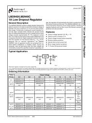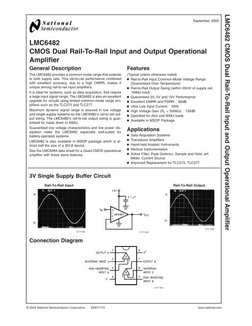
Lmc6482 cmos dual rail-to-rail input and output operational amplifier
Lmc6482 cmos dual rail-to-rail input and output operational amplifier
Lmc6482 cmos dual rail-to-rail input and output operational amplifier

You also want an ePaper? Increase the reach of your titles
YUMPU automatically turns print PDFs into web optimized ePapers that Google loves.
LMC6482<br />
CMOS Dual Rail-To-Rail Input <strong>and</strong> Output Operational<br />
Amplifier<br />
General Description<br />
The LMC6482 provides a common-mode range that extends<br />
<strong>to</strong> both supply <strong>rail</strong>s. This <strong>rail</strong>-<strong>to</strong>-<strong>rail</strong> performance combined<br />
with excellent accuracy, due <strong>to</strong> a high CMRR, makes it<br />
unique among <strong>rail</strong>-<strong>to</strong>-<strong>rail</strong> <strong>input</strong> <strong>amplifier</strong>s.<br />
It is ideal for systems, such as data acquisition, that require<br />
a large <strong>input</strong> signal range. The LMC6482 is also an excellent<br />
upgrade for circuits using limited common-mode range <strong>amplifier</strong>s<br />
such as the TLC272 <strong>and</strong> TLC277.<br />
Maximum dynamic signal range is assured in low voltage<br />
<strong>and</strong> single supply systems by the LMC6482’s <strong>rail</strong>-<strong>to</strong>-<strong>rail</strong> <strong>output</strong><br />
swing. The LMC6482’s <strong>rail</strong>-<strong>to</strong>-<strong>rail</strong> <strong>output</strong> swing is guaranteed<br />
for loads down <strong>to</strong> 600Ω.<br />
Guaranteed low voltage characteristics <strong>and</strong> low power dissipation<br />
make the LMC6482 especially well-suited for<br />
battery-operated systems.<br />
LMC6482 is also available in MSOP package which is almost<br />
half the size of a SO-8 device.<br />
See the LMC6484 data sheet for a Quad CMOS <strong>operational</strong><br />
<strong>amplifier</strong> with these same features.<br />
3V Single Supply Buffer Circuit<br />
Rail-To-Rail Input<br />
Features<br />
01171301 01171302<br />
(Typical unless otherwise noted)<br />
n Rail-<strong>to</strong>-Rail Input Common-Mode Voltage Range<br />
(Guaranteed Over Temperature)<br />
n Rail-<strong>to</strong>-Rail Output Swing (within 20mV of supply <strong>rail</strong>,<br />
100kΩ load)<br />
n Guaranteed 3V, 5V <strong>and</strong> 15V Performance<br />
n Excellent CMRR <strong>and</strong> PSRR: 82dB<br />
n Ultra Low Input Current: 20fA<br />
n High Voltage Gain (R L = 500kΩ): 130dB<br />
n Specified for 2kΩ <strong>and</strong> 600Ω loads<br />
n Available in MSOP Package<br />
Applications<br />
n Data Acquisition Systems<br />
n Transducer Amplifiers<br />
n H<strong>and</strong>-held Analytic Instruments<br />
n Medical Instrumentation<br />
n Active Filter, Peak Detec<strong>to</strong>r, Sample <strong>and</strong> Hold, pH<br />
Meter, Current Source<br />
n Improved Replacement for TLC272, TLC277<br />
Rail-To-Rail Output<br />
September 2003<br />
01171303<br />
LMC6482 CMOS Dual Rail-To-Rail Input <strong>and</strong> Output Operational Amplifier<br />
Connection Diagram<br />
01171304<br />
© 2004 National Semiconduc<strong>to</strong>r Corporation DS011713 www.national.com
LMC6482<br />
Absolute Maximum Ratings (Note 1)<br />
If Military/Aerospace specified devices are required,<br />
please contact the National Semiconduc<strong>to</strong>r Sales Office/<br />
Distribu<strong>to</strong>rs for availability <strong>and</strong> specifications.<br />
ESD Tolerance (Note 2)<br />
Differential Input Voltage<br />
Voltage at Input/Output Pin<br />
Supply Voltage (V + −V − )<br />
Current at Input Pin (Note 12)<br />
Current at Output Pin<br />
(Notes 3, 8)<br />
Current at Power Supply Pin<br />
Lead Temperature<br />
(Soldering, 10 sec.)<br />
S<strong>to</strong>rage Temperature Range<br />
1.5kV<br />
±Supply Voltage<br />
(V + ) +0.3V, (V − ) −0.3V<br />
16V<br />
±5mA<br />
±30mA<br />
40mA<br />
260˚C<br />
−65˚C <strong>to</strong> +150˚C<br />
Junction Temperature (Note 4)<br />
Operating Ratings (Note 1)<br />
150˚C<br />
Supply Voltage 3.0V ≤ V+ ≤ 15.5V<br />
Junction Temperature Range<br />
LMC6482AM<br />
−55˚C ≤ T J ≤<br />
+125˚C<br />
LMC6482AI, LMC6482I<br />
−40˚C ≤ T J ≤ +85˚C<br />
Thermal Resistance (θ JA )<br />
N Package, 8-Pin Molded DIP<br />
90˚C/W<br />
M Package, 8-Pin Surface<br />
Mount<br />
155˚C/W<br />
MSOP package, 8-Pin Mini SO<br />
194˚C/W<br />
DC Electrical Characteristics<br />
Unless otherwise specified, all limits guaranteed for T J = 25˚C, V + = 5V, V − = 0V, V CM =V O =V + /2 <strong>and</strong> R L<br />
> 1M. Boldface<br />
limits apply at the temperature extremes.<br />
Symbol Parameter Conditions Typ LMC6482AI LMC6482I LMC6482M Units<br />
(Note 5) Limit Limit Limit<br />
(Note 6) (Note 6) (Note 6)<br />
V OS Input Offset Voltage 0.11 0.750 3.0 3.0 mV<br />
1.35 3.7 3.8 max<br />
TCV OS Input Offset Voltage 1.0 µV/˚C<br />
Average Drift<br />
I B Input Current (Note 13) 0.02 4.0 4.0 10.0 pA<br />
max<br />
I OS Input Offset Current (Note 13) 0.01 2.0 2.0 5.0 pA<br />
max<br />
C IN Common-Mode 3 pF<br />
Input Capacitance<br />
R IN Input Resistance >10 TeraΩ<br />
CMRR Common Mode 0V ≤ V CM ≤ 15.0V 82 70 65 65 dB<br />
Rejection Ratio V + = 15V 67 62 60 min<br />
0V ≤ V CM ≤ 5.0V 82 70 65 65<br />
V + =5V 67 62 60<br />
+PSRR Positive Power Supply 5V ≤ V + ≤ 15V, V − = 0V 82 70 65 65 dB<br />
Rejection Ratio V O = 2.5V 67 62 60 min<br />
−PSRR Negative Power Supply −5V ≤ V − ≤ −15V, V + = 0V 82 70 65 65 dB<br />
Rejection Ratio V O = −2.5V 67 62 60 min<br />
V CM Input Common-Mode V + = 5V <strong>and</strong> 15V V − − 0.3 − 0.25 − 0.25 − 0.25 V<br />
Voltage Range For CMRR ≥ 50dB 0 0 0 max<br />
V + + 0.3V V + + 0.25 V + + 0.25 V + + 0.25 V<br />
V + V + V + min<br />
A V Large Signal R L =2kΩ Sourcing 666 140 120 120 V/mV<br />
Voltage Gain (Notes 7, 13) 84 72 60 min<br />
Sinking 75 35 35 35 V/mV<br />
20 20 18 min<br />
R L = 600Ω Sourcing 300 80 50 50 V/mV<br />
(Notes 7, 13) 48 30 25 min<br />
Sinking 35 20 15 15 V/mV<br />
www.national.com 2
DC Electrical Characteristics (Continued)<br />
Unless otherwise specified, all limits guaranteed for T J = 25˚C, V + = 5V, V − = 0V, V CM =V O =V + /2 <strong>and</strong> R L<br />
> 1M. Boldface<br />
limits apply at the temperature extremes.<br />
Symbol Parameter Conditions Typ LMC6482AI LMC6482I LMC6482M Units<br />
(Note 5) Limit Limit Limit<br />
(Note 6) (Note 6) (Note 6)<br />
13 10 8 min<br />
V O Output Swing V + = 5V 4.9 4.8 4.8 4.8 V<br />
R L =2kΩ <strong>to</strong> V + /2 4.7 4.7 4.7 min<br />
0.1 0.18 0.18 0.18 V<br />
0.24 0.24 0.24 max<br />
V + = 5V 4.7 4.5 4.5 4.5 V<br />
R L = 600Ω <strong>to</strong> V + /2 4.24 4.24 4.24 min<br />
0.3 0.5 0.5 0.5 V<br />
0.65 0.65 0.65 max<br />
V + = 15V 14.7 14.4 14.4 14.4 V<br />
R L =2kΩ <strong>to</strong> V + /2 14.2 14.2 14.2 min<br />
0.16 0.32 0.32 0.32 V<br />
0.45 0.45 0.45 max<br />
V + = 15V 14.1 13.4 13.4 13.4 V<br />
R L = 600Ω <strong>to</strong> V + /2 13.0 13.0 13.0 min<br />
0.5 1.0 1.0 1.0 V<br />
1.3 1.3 1.3 max<br />
I SC Output Short Circuit Sourcing, V O = 0V 20 16 16 16 mA<br />
Current 12 12 10 min<br />
V + = 5V Sinking, V O = 5V 15 11 11 11 mA<br />
9.5 9.5 8.0 min<br />
I SC Output Short Circuit Sourcing, V O = 0V 30 28 28 28 mA<br />
Current 22 22 20 min<br />
V + = 15V Sinking, V O = 12V 30 30 30 30 mA<br />
(Note 8) 24 24 22 min<br />
I S Supply Current Both Amplifiers 1.0 1.4 1.4 1.4 mA<br />
V + = +5V, V O =V + /2 1.8 1.8 1.9 max<br />
Both Amplifiers 1.3 1.6 1.6 1.6 mA<br />
V + = 15V, V O =V + /2 1.9 1.9 2.0 max<br />
LMC6482<br />
AC Electrical Characteristics<br />
Unless otherwise specified, all limits guaranteed for T J = 25˚C, V + = 5V, V − = 0V, V CM =V O =V + /2, <strong>and</strong> R L<br />
> 1M. Boldface<br />
limits apply at the temperature extremes.<br />
Symbol Parameter Conditions Typ LMC6482AI LMC6482I LMC6482M Units<br />
(Note 5) Limit Limit Limit<br />
(Note 6) (Note 6) (Note 6)<br />
SR Slew Rate (Note 9) 1.3 1.0 0.9 0.9 V/µs<br />
0.7 0.63 0.54 min<br />
GBW Gain-B<strong>and</strong>width Product V + = 15V 1.5 MHz<br />
φ m Phase Margin 50 Deg<br />
G m Gain Margin 15 dB<br />
Amp-<strong>to</strong>-Amp Isolation (Note 10) 150 dB<br />
e n Input-Referred F = 1kHz 37 nV/√Hz<br />
Voltage Noise V cm =1V<br />
i n Input-Referred F = 1kHz 0.03 pA/√Hz<br />
Current Noise<br />
3<br />
www.national.com
LMC6482<br />
AC Electrical Characteristics (Continued)<br />
Unless otherwise specified, all limits guaranteed for T J = 25˚C, V + = 5V, V − = 0V, V CM =V O =V + /2, <strong>and</strong> R L<br />
> 1M. Boldface<br />
limits apply at the temperature extremes.<br />
Symbol Parameter Conditions Typ LMC6482AI LMC6482I LMC6482M Units<br />
(Note 5) Limit Limit Limit<br />
(Note 6) (Note 6) (Note 6)<br />
T.H.D. Total Harmonic Dis<strong>to</strong>rtion F = 10kHz, A V =−2 %<br />
R L = 10kΩ, V O = 4.1 V PP 0.01<br />
F = 10kHz, A V =−2<br />
R L = 10kΩ, V O = 8.5 V PP 0.01 %<br />
V + = 10V<br />
DC Electrical Characteristics<br />
Unless otherwise specified, all limits guaranteed for T J = 25˚C, V + = 3V, V − = 0V, V CM =V O =V + /2 <strong>and</strong> R L<br />
> 1M.<br />
Symbol Parameter Conditions Typ LMC6482AI LMC6482I LMC6482M Units<br />
(Note 5) Limit Limit Limit<br />
(Note 6) (Note 6) (Note 6)<br />
V OS Input Offset Voltage 0.9 2.0 3.0 3.0 mV<br />
2.7 3.7 3.8 max<br />
TCV OS Input Offset Voltage 2.0 µV/˚C<br />
Average Drift<br />
I B Input Bias Current 0.02 pA<br />
I OS Input Offset Current 0.01 pA<br />
CMRR Common Mode 0V ≤ V CM ≤ 3V 74 64 60 60 dB<br />
Rejection Ratio<br />
min<br />
PSRR Power Supply 3V ≤ V + ≤ 15V, V − = 0V 80 68 60 60 dB<br />
Rejection Ratio<br />
min<br />
V CM Input Common-Mode For CMRR ≥ 50dB V − −0.25 0 0 0 V<br />
Voltage Range<br />
max<br />
V + + 0.25 V + V + V + V<br />
min<br />
V O Output Swing R L =2kΩ <strong>to</strong> V + /2 2.8 V<br />
0.2 V<br />
R L = 600Ω <strong>to</strong> V + /2 2.7 2.5 2.5 2.5 V<br />
min<br />
0.37 0.6 0.6 0.6 V<br />
max<br />
I S Supply Current Both Amplifiers 0.825 1.2 1.2 1.2 mA<br />
1.5 1.5 1.6 max<br />
AC Electrical Characteristics<br />
Unless otherwise specified, V + = 3V, V − = 0V, V CM =V O =V + /2, <strong>and</strong> R L<br />
> 1M.<br />
Symbol Parameter Conditions Typ LMC6482AI LMC6482I LMC6482M Units<br />
(Note 5) Limit Limit Limit<br />
(Note 6) (Note 6) (Note 6)<br />
SR Slew Rate (Note 11) 0.9 V/µs<br />
GBW Gain-B<strong>and</strong>width Product 1.0 MHz<br />
T.H.D. Total Harmonic Dis<strong>to</strong>rtion F = 10kHz, A V = −2 0.01 %<br />
R L = 10kΩ, V O =2V PP<br />
Note 1: Absolute Maximum Ratings indicate limts beyond which damage <strong>to</strong> the device may occur. Operating Ratings indicate conditions for which the device is<br />
intended <strong>to</strong> be functional, but specific performance is not guaranteed. For guaranteed specifications <strong>and</strong> the test conditions, see the Electrical Characteristics.<br />
Note 2: Human body model, 1.5kΩ in series with 100pF. All pins rated per method 3015.6 of MIL-STD-883. This is a Class 1 device rating.<br />
www.national.com 4
AC Electrical Characteristics (Continued)<br />
Note 3: Applies <strong>to</strong> both single-supply <strong>and</strong> split-supply operation. Continuous short circuit operation at elevated ambient temperature can result in exceeding the<br />
maximum allowed junction temperature of 150˚C. Output currents in excess of ±30mA over long term may adversely affect reliability.<br />
Note 4: The maximum power dissipation is a function of T J(max) , θ JA , <strong>and</strong> T A . The maximum allowable power dissipation at any ambient temperature is P D =(T J(max)<br />
−T A )/θ JA . All numbers apply for packages soldered directly in<strong>to</strong> a PC board.<br />
Note 5: Typical Values represent the most likely parametric norm.<br />
Note 6: All limits are guaranteed by testing or statistical analysis.<br />
Note 7: V + = 15V, V CM = 7.5V <strong>and</strong> R L connected <strong>to</strong> 7.5V. For Sourcing tests, 7.5V ≤ V O ≤ 11.5V. For Sinking tests, 3.5V ≤ V O ≤ 7.5V.<br />
Note 8: Do not short circuit <strong>output</strong> <strong>to</strong> V + , when V + is greater than 13V or reliability will be adversely affected.<br />
Note 9: V + = 15V. Connected as Voltage Follower with 10V step <strong>input</strong>. Number specified is the slower of either the positive or negative slew rates.<br />
Note 10: Input referred, V + = 15V <strong>and</strong> R L = 100 kΩ connected <strong>to</strong> 7.5V. Each amp excited in turn with 1 kHz <strong>to</strong> produce V O =12V PP .<br />
Note 11: Connected as voltage Follower with 2V step <strong>input</strong>. Number specified is the slower of either the positive or negative slew rates.<br />
Note 12: Limiting <strong>input</strong> pin current is only necessary for <strong>input</strong> voltages that exceed absolute maximum <strong>input</strong> voltage ratings.<br />
Note 13: Guaranteed limits are dictated by tester limitations <strong>and</strong> not device performance. Actual performance is reflected in the typical value.<br />
Note 14: For guaranteed Military Temperature parameters see RETS6482X.<br />
LMC6482<br />
Typical Performance Characteristics<br />
V S = +15V, Single Supply, T A = 25˚C unless otherwise<br />
specified<br />
Supply Current vs. Supply Voltage<br />
Input Current vs. Temperature<br />
01171340<br />
01171341<br />
Sourcing Current vs. Output Voltage<br />
Sourcing Current vs. Output Voltage<br />
01171342 01171343<br />
5<br />
www.national.com
LMC6482<br />
Typical Performance Characteristics V S = +15V, Single Supply, T A = 25˚C unless otherwise<br />
specified (Continued)<br />
Sourcing Current vs. Output Voltage<br />
Sinking Current vs. Output Voltage<br />
01171344 01171345<br />
Sinking Current vs. Output Voltage<br />
Sinking Current vs. Output Voltage<br />
01171346 01171347<br />
Output Voltage Swing vs. Supply Voltage<br />
Input Voltage Noise vs. Frequency<br />
01171348<br />
01171349<br />
www.national.com 6
Typical Performance Characteristics V S = +15V, Single Supply, T A = 25˚C unless otherwise<br />
specified (Continued)<br />
Input Voltage Noise vs. Input Voltage<br />
Input Voltage Noise vs. Input Voltage<br />
LMC6482<br />
01171350 01171351<br />
Input Voltage Noise vs. Input Voltage<br />
Crosstalk Rejection vs. Frequency<br />
01171352<br />
01171353<br />
Crosstalk Rejection vs. Frequency<br />
Positive PSRR vs. Frequency<br />
01171354 01171355<br />
7<br />
www.national.com
LMC6482<br />
Typical Performance Characteristics V S = +15V, Single Supply, T A = 25˚C unless otherwise<br />
specified (Continued)<br />
Negative PSRR vs. Frequency<br />
CMRR vs. Frequency<br />
01171356 01171357<br />
CMRR vs. Input Voltage<br />
CMRR vs. Input Voltage<br />
01171358 01171359<br />
CMRR vs. Input Voltage<br />
∆V OS vs. CMR<br />
01171360 01171361<br />
www.national.com 8
Typical Performance Characteristics V S = +15V, Single Supply, T A = 25˚C unless otherwise<br />
specified (Continued)<br />
∆V OS vs. CMR<br />
Input Voltage vs. Output Voltage<br />
LMC6482<br />
01171362 01171363<br />
Input Voltage vs. Output Voltage<br />
Open Loop Frequency Response<br />
01171364<br />
01171365<br />
Open Loop Frequency Responce<br />
Open Loop Frequency Response vs. Temperature<br />
01171366 01171367<br />
9<br />
www.national.com
LMC6482<br />
Typical Performance Characteristics V S = +15V, Single Supply, T A = 25˚C unless otherwise<br />
specified (Continued)<br />
Maximum Output Swing vs. Frequency<br />
Gain <strong>and</strong> Phase vs. Capacitive Load<br />
01171368<br />
01171369<br />
Gain <strong>and</strong> Phase vs. Capacitive Load<br />
Open Loop Output Impedance vs. Frequency<br />
01171370 01171371<br />
Open Loop Output Impedance vs. Frequency<br />
Slew Rate vs. Supply Voltage<br />
01171372<br />
01171373<br />
www.national.com 10
Typical Performance Characteristics V S = +15V, Single Supply, T A = 25˚C unless otherwise<br />
specified (Continued)<br />
Non-Inverting Large Signal Pulse Response<br />
Non-Inverting Large Signal Pulse Response<br />
LMC6482<br />
01171374 01171375<br />
Non-Inverting Large Signal Pulse Response<br />
Non-Inverting Small Signal Pulse Response<br />
01171376 01171377<br />
Non-Inverting Small Signal Pulse Response<br />
Non-Inverting Small Signal Pulse Response<br />
01171378 01171379<br />
11<br />
www.national.com
LMC6482<br />
Typical Performance Characteristics V S = +15V, Single Supply, T A = 25˚C unless otherwise<br />
specified (Continued)<br />
Inverting Large Signal Pulse Response<br />
Inverting Large Signal Pulse Response<br />
01171380 01171381<br />
Inverting Large Signal Pulse Response<br />
Inverting Small Signal Pulse Response<br />
01171382 01171383<br />
Inverting Small Signal Pulse Response<br />
Inverting Small Signal Pulse Response<br />
01171384 01171385<br />
www.national.com 12
Typical Performance Characteristics V S = +15V, Single Supply, T A = 25˚C unless otherwise<br />
specified (Continued)<br />
Stability vs. Capacitive Load<br />
Stability vs. Capacitive Load<br />
LMC6482<br />
01171386 01171387<br />
Stability vs. Capacitive Load<br />
Stability vs. Capacitive Load<br />
01171388 01171389<br />
Stability vs. Capacitive Load<br />
Stability vs. Capacitive Load<br />
01171390 01171391<br />
13<br />
www.national.com
LMC6482<br />
Application Information<br />
1.0 AMPLIFIER TOPOLOGY<br />
The LMC6482 incorporates specially designed widecompliance<br />
range current mirrors <strong>and</strong> the body effect <strong>to</strong><br />
extend <strong>input</strong> common mode range <strong>to</strong> each supply <strong>rail</strong>.<br />
Complementary paralleled differential <strong>input</strong> stages, like the<br />
type used in other CMOS <strong>and</strong> bipolar <strong>rail</strong>-<strong>to</strong>-<strong>rail</strong> <strong>input</strong> <strong>amplifier</strong>s,<br />
were not used because of their inherent accuracy<br />
problems due <strong>to</strong> CMRR, cross-over dis<strong>to</strong>rtion, <strong>and</strong> openloop<br />
gain variation.<br />
The LMC6482’s <strong>input</strong> stage design is complemented by an<br />
<strong>output</strong> stage capable of <strong>rail</strong>-<strong>to</strong>-<strong>rail</strong> <strong>output</strong> swing even when<br />
driving a large load. Rail-<strong>to</strong>-<strong>rail</strong> <strong>output</strong> swing is obtained by<br />
taking the <strong>output</strong> directly from the internal integra<strong>to</strong>r instead<br />
of an <strong>output</strong> buffer stage.<br />
2.0 INPUT COMMON-MODE VOLTAGE RANGE<br />
Unlike Bi-FET <strong>amplifier</strong> designs, the LMC6482 does not<br />
exhibit phase inversion when an <strong>input</strong> voltage exceeds the<br />
negative supply voltage. Figure 1 shows an <strong>input</strong> voltage<br />
exceeding both supplies with no resulting phase inversion on<br />
the <strong>output</strong>.<br />
01171339<br />
FIGURE 2. A ±7.5V Input Signal Greatly<br />
Exceeds the 3V Supply in Figure 3 Causing<br />
No Phase Inversion Due <strong>to</strong> R I<br />
Applications that exceed this rating must externally limit the<br />
maximum <strong>input</strong> current <strong>to</strong> ±5mA with an <strong>input</strong> resis<strong>to</strong>r (R I )as<br />
shown in Figure 3.<br />
01171311<br />
FIGURE 3. R I Input Current Protection for<br />
Voltages Exceeding the Supply Voltages<br />
01171310<br />
FIGURE 1. An Input Voltage Signal Exceeds the<br />
LMC6482 Power Supply Voltages with<br />
No Output Phase Inversion<br />
The absolute maximum <strong>input</strong> voltage is 300mV beyond either<br />
supply <strong>rail</strong> at room temperature. Voltages greatly exceeding<br />
this absolute maximum rating, as in Figure 2, can<br />
cause excessive current <strong>to</strong> flow in or out of the <strong>input</strong> pins<br />
possibly affecting reliability.<br />
3.0 RAIL-TO-RAIL OUTPUT<br />
The approximated <strong>output</strong> resistance of the LMC6482 is<br />
180Ω sourcing <strong>and</strong> 130Ω sinking at V S = 3V <strong>and</strong> 110Ω<br />
sourcing <strong>and</strong> 80Ω sinking at Vs = 5V. Using the calculated<br />
<strong>output</strong> resistance, maximum <strong>output</strong> voltage swing can be<br />
estimated as a function of load.<br />
4.0 CAPACITIVE LOAD TOLERANCE<br />
The LMC6482 can typically directly drive a 100pF load with<br />
V S = 15V at unity gain without oscillating. The unity gain<br />
follower is the most sensitive configuration. Direct capacitive<br />
loading reduces the phase margin of op-amps. The combination<br />
of the op-amp’s <strong>output</strong> impedance <strong>and</strong> the capacitive<br />
load induces phase lag. This results in either an underdamped<br />
pulse response or oscillation.<br />
Capacitive load compensation can be accomplished using<br />
resistive isolation as shown in Figure 4. This simple technique<br />
is useful for isolating the capacitive <strong>input</strong>s of multiplexers<br />
<strong>and</strong> A/D converters.<br />
www.national.com 14
Application Information (Continued)<br />
LMC6482<br />
01171317<br />
FIGURE 4. Resistive Isolation<br />
of a 330pF Capacitive Load<br />
01171316<br />
FIGURE 7. Pulse Response of<br />
LMC6482 Circuit in Figure 6<br />
5.0 COMPENSATING FOR INPUT CAPACITANCE<br />
It is quite common <strong>to</strong> use large values of feedback resistance<br />
with <strong>amplifier</strong>s that have ultra-low <strong>input</strong> current, like<br />
the LMC6482. Large feedback resis<strong>to</strong>rs can react with small<br />
values of <strong>input</strong> capacitance due <strong>to</strong> transducers, pho<strong>to</strong>diodes,<br />
<strong>and</strong> circuits board parasitics <strong>to</strong> reduce phase margins.<br />
01171318<br />
FIGURE 5. Pulse Response of<br />
the LMC6482 Circuit in Figure 4<br />
Improved frequency response is achieved by indirectly driving<br />
capacitive loads, as shown in Figure 6.<br />
01171319<br />
FIGURE 8. Canceling the Effect of Input Capacitance<br />
The effect of <strong>input</strong> capacitance can be compensated for by<br />
adding a feedback capaci<strong>to</strong>r. The feedback capaci<strong>to</strong>r (as in<br />
Figure 8), C f , is first estimated by:<br />
01171315<br />
FIGURE 6. LMC6482 Noninverting Amplifier,<br />
Compensated <strong>to</strong> H<strong>and</strong>le a 330pF Capacitive Load<br />
R1 <strong>and</strong> C1 serve <strong>to</strong> counteract the loss of phase margin by<br />
feeding forward the high frequency component of the <strong>output</strong><br />
signal back <strong>to</strong> the <strong>amplifier</strong>s inverting <strong>input</strong>, thereby preserving<br />
phase margin in the overall feedback loop. The values of<br />
R1 <strong>and</strong> C1 are experimentally determined for the desired<br />
pulse response. The resulting pulse response can be seen in<br />
Figure 7.<br />
or<br />
R 1 C IN ≤ R 2 C f<br />
which typically provides significant overcompensation.<br />
Printed circuit board stray capacitance may be larger or<br />
smaller than that of a bread-board, so the actual optimum<br />
value for C f may be different. The values of C f should be<br />
checked on the actual circuit. (Refer <strong>to</strong> the LMC660 quad<br />
CMOS <strong>amplifier</strong> data sheet for a more detailed discussion.)<br />
15<br />
www.national.com
LMC6482<br />
Application Information (Continued)<br />
6.0 PRINTED-CIRCUIT-BOARD LAYOUT FOR<br />
HIGH-IMPEDANCE WORK<br />
It is generally recognized that any circuit which must operrate<br />
with less than 1000pA of leakage current requires special<br />
layout of the PC board. When one wishes <strong>to</strong> take advantage<br />
of the ultra-low <strong>input</strong> current of the LMC6482,<br />
typically less than 20fA, it is essential <strong>to</strong> have an excellent<br />
layout. Fortunately, the techniques of obtaining low leakages<br />
are quite simple. First, the user must not ignore the surface<br />
leakage of the PC board, even through it may sometimes<br />
appear acceptably low, because under conditions of high<br />
humidity or dust or contamination, the surface leakage will<br />
be appreciable.<br />
To minimize the effect of any surface leakage, lay out a ring<br />
of foil completely surrounding the LM6482’s <strong>input</strong>s <strong>and</strong> the<br />
terminals of capaci<strong>to</strong>rs, diodes, conduc<strong>to</strong>rs, resis<strong>to</strong>rs, relay<br />
terminals, etc. connected <strong>to</strong> the op-amp’s <strong>input</strong>s, as in Figure<br />
9. To have a significant effect, guard rings should be<br />
placed on both the <strong>to</strong>p <strong>and</strong> bot<strong>to</strong>m of the PC board. This PC<br />
foil must then be connected <strong>to</strong> a voltage which is at the same<br />
voltage as the <strong>amplifier</strong> <strong>input</strong>s, since no leakage current can<br />
flow between two points at the same potential. For example,<br />
a PC board trace-<strong>to</strong>-pad resistance of 10 12 Ω, which is normally<br />
considered a very large resistance, could leak 5pA if<br />
the trace were a 5V bus adjacent <strong>to</strong> the pad of the <strong>input</strong>. This<br />
would cause a 250 times degradation from the LMC6482’s<br />
actual performance. However, if a guard ring is held within 5<br />
mV of the <strong>input</strong>s, then even a resistance of 10 11 Ω would<br />
cause only 0.05pA of leakage current. See Figure 10 for<br />
typical connections of guard rings for st<strong>and</strong>ard op-amp configurations.<br />
Inverting Amplifier<br />
Non-Inverting Amplifier<br />
01171321<br />
01171322<br />
Follower<br />
01171323<br />
FIGURE 10. Typical Connections of Guard Rings<br />
The designer should be aware that when it is inappropriate<br />
<strong>to</strong> lay out a PC board for the sake of just a few circuits, there<br />
is another technique which is even better than a guard ring<br />
on a PC board: Don’t insert the <strong>amplifier</strong>’s <strong>input</strong> pin in<strong>to</strong> the<br />
board at all, but bend it up in the air <strong>and</strong> use only air as an<br />
insula<strong>to</strong>r. Air is an excellent insula<strong>to</strong>r. In this case you may<br />
have <strong>to</strong> forego some of the advantages of PC board construction,<br />
but the advantages are sometimes well worth the<br />
effort of using point-<strong>to</strong>-point up-in-the-air wiring.<br />
See Figure 11.<br />
01171320<br />
FIGURE 9. Example of Guard Ring in P.C. Board<br />
Layout<br />
01171324<br />
(Input pins are lifted out of PC board <strong>and</strong> soldered directly <strong>to</strong> components.<br />
All other pins connected <strong>to</strong> PC board.)<br />
FIGURE 11. Air Wiring<br />
www.national.com 16
Application Information (Continued)<br />
7.0 OFFSET VOLTAGE ADJUSTMENT<br />
Offset voltage adjustment circuits are illustrated in Figure 12<br />
Figure 13. Large value resistances <strong>and</strong> potentiometers are<br />
used <strong>to</strong> reduce power consumption while providing typically<br />
±2.5mV of adjustment range, referred <strong>to</strong> the <strong>input</strong>, for both<br />
configurations with V S = ±5V.<br />
01171325<br />
8.0 UPGRADING APPLICATIONS<br />
The LMC6484 quads <strong>and</strong> LMC6482 <strong>dual</strong>s have industry<br />
st<strong>and</strong>ard pin outs <strong>to</strong> retrofit existing applications. System<br />
performance can be greatly increased by the LMC6482’s<br />
features. The key benefit of designing in the LMC6482 is<br />
increased linear signal range. Most op-amps have limited<br />
<strong>input</strong> common mode ranges. Signals that exceed this range<br />
generate a non-linear <strong>output</strong> response that persists long<br />
after the <strong>input</strong> signal returns <strong>to</strong> the common mode range.<br />
Linear signal range is vital in applications such as filters<br />
where signal peaking can exceed <strong>input</strong> common mode<br />
ranges resulting in <strong>output</strong> phase inverison or severe dis<strong>to</strong>rtion.<br />
9.0 DATA ACQUISITION SYSTEMS<br />
Low power, single supply data acquisition system solutions<br />
are provided by buffering the ADC12038 with the LMC6482<br />
(Figure 14). Capable of using the full supply range, the<br />
LMC6482 does not require <strong>input</strong> signals <strong>to</strong> be scaled down<br />
<strong>to</strong> meet limited common mode voltage ranges. The<br />
LMC4282 CMRR of 82dB maintains integral linearity of a<br />
12-bit data acquisition system <strong>to</strong> ±0.325 LSB. Other <strong>rail</strong>-<strong>to</strong><strong>rail</strong><br />
<strong>input</strong> <strong>amplifier</strong>s with only 50dB of CMRR will degrade the<br />
accuracy of the data acquisition system <strong>to</strong> only 8 bits.<br />
LMC6482<br />
FIGURE 12. Inverting Configuration<br />
Offset Voltage Adjustment<br />
01171326<br />
FIGURE 13. Non-Inverting Configuration<br />
Offset Voltage Adjustment<br />
17<br />
www.national.com
LMC6482<br />
Application Information (Continued)<br />
01171328<br />
FIGURE 14. Operating from the same<br />
Supply Voltage, the LMC6482 buffers the<br />
ADC12038 maintaining excellent accuracy<br />
10.0 INSTRUMENTATION CIRCUITS<br />
The LMC6482 has the high <strong>input</strong> impedance, large commonmode<br />
range <strong>and</strong> high CMRR needed for designing instrumentation<br />
circuits. Instrumentation circuits designed with the<br />
LMC6482 can reject a larger range of common-mode signals<br />
than most in-amps. This makes instrumentation circuits designed<br />
with the LMC6482 an excellent choice of noisy or<br />
industrial environments. Other applications that benefit from<br />
these features include analytic medical instruments, magnetic<br />
field detec<strong>to</strong>rs, gas detec<strong>to</strong>rs, <strong>and</strong> silicon-based<br />
tr<strong>and</strong>ucers.<br />
A small valued potentiometer is used in series with R g <strong>to</strong> set<br />
the differential gain of the 3 op-amp instrumentation circuit in<br />
Figure 15. This combination is used instead of one large<br />
valued potentiometer <strong>to</strong> increase gain trim accuracy <strong>and</strong><br />
reduce error due <strong>to</strong> vibration.<br />
www.national.com 18
Application Information (Continued)<br />
LMC6482<br />
01171329<br />
FIGURE 15. Low Power 3 Op-Amp Instrumentation Amplifier<br />
A 2 op-amp instrumentation <strong>amplifier</strong> designed for a gain of<br />
100 is shown in Figure 16. Low sensitivity trimming is made<br />
for offset voltage, CMRR <strong>and</strong> gain. Low cost <strong>and</strong> low power<br />
consumption are the main advantages of this two op-amp<br />
circuit.<br />
Higher frequency <strong>and</strong> larger common-mode range applications<br />
are best facilitated by a three op-amp instrumentation<br />
<strong>amplifier</strong>.<br />
01171330<br />
FIGURE 16. Low-Power Two-Op-Amp Instrumentation Amplifier<br />
11.0 SPICE MACROMODEL<br />
A spice macromodel is available for the LMC6482. This<br />
model includes accurate simulation of:<br />
• Input common-mode voltage range<br />
• Frequency <strong>and</strong> transient response<br />
• GBW dependence on loading conditions<br />
• Quiescent <strong>and</strong> dynamic supply current<br />
• Output swing dependence on loading conditions<br />
<strong>and</strong> many more characteristics as listed on the macromodel<br />
disk.<br />
Contact your local National Semiconduc<strong>to</strong>r sales office <strong>to</strong><br />
obtain an <strong>operational</strong> <strong>amplifier</strong> spice model library disk.<br />
19<br />
www.national.com
LMC6482<br />
Typical Single-Supply Applications<br />
The circuit in Figure 17 uses a single supply <strong>to</strong> half wave<br />
rectify a sinusoid centered about ground. R I limits current<br />
in<strong>to</strong> the <strong>amplifier</strong> caused by the <strong>input</strong> voltage exceeding the<br />
supply voltage. Full wave rectification is provided by the<br />
circuit in Figure 19.<br />
01171331<br />
FIGURE 17. Half-Wave Rectifier<br />
with Input Current Protection (RI)<br />
01171333<br />
FIGURE 19. Full Wave Rectifier<br />
with Input Current Protection (R I )<br />
01171332<br />
FIGURE 18. Half-Wave Rectifier Waveform<br />
01171334<br />
FIGURE 20. Full Wave Rectifier Waveform<br />
www.national.com 20
Typical Single-Supply Applications<br />
(Continued)<br />
LMC6482<br />
01171336<br />
01171335<br />
FIGURE 22. Positive Supply Current Sense<br />
FIGURE 21. Large Compliance Range Current Source<br />
01171337<br />
FIGURE 23. Low Voltage Peak Detec<strong>to</strong>r with Rail-<strong>to</strong>-Rail Peak Capture Range<br />
In Figure 23 dielectric absorption <strong>and</strong> leakage is minimized<br />
by using a polystyrene or polyethylene hold capaci<strong>to</strong>r. The<br />
droop rate is primarily determined by the value of C H <strong>and</strong><br />
diode leakage current. The ultra-low <strong>input</strong> current of the<br />
LMC6482 has a negligible effect on droop.<br />
01171338<br />
FIGURE 24. Rail-<strong>to</strong>-Rail Sample <strong>and</strong> Hold<br />
The LMC6482’s high CMRR (82dB) allows excellent accuracy<br />
throughout the circuit’s <strong>rail</strong>-<strong>to</strong>-<strong>rail</strong> dynamic capture<br />
range.<br />
21<br />
www.national.com
LMC6482<br />
Typical Single-Supply Applications (Continued)<br />
01171327<br />
FIGURE 25. Rail-<strong>to</strong>-Rail Single Supply Low Pass Filter<br />
The low pass filter circuit in Figure 25 can be used as an<br />
anti-aliasing filter with the same voltage supply as the A/D<br />
converter.<br />
Filter designs can also take advantage of the LMC6482<br />
ultra-low <strong>input</strong> current. The ultra-low <strong>input</strong> current yields<br />
negligible offset error even when large value resis<strong>to</strong>rs are<br />
used. This in turn allows the use of smaller valued capaci<strong>to</strong>rs<br />
which take less board space <strong>and</strong> cost less.<br />
Ordering Information<br />
Package Temperature Range NSC Transport<br />
Package Marking<br />
Military Industrial Drawing Media<br />
−55˚C <strong>to</strong> +125˚C −40˚C <strong>to</strong> +85˚C<br />
8-Pin LMC6482AIN, N08E Rail LMC6482MN,<br />
Molded DIP LMC6482IN LMC6482AIN, LMC6482IN<br />
8-pin<br />
LMC6482AIM,<br />
Rail LMC6482AIM, LMC6482IM<br />
M08A<br />
LMC6482AIMX<br />
Small Outline<br />
LMC6482IM,<br />
Tape <strong>and</strong> Reel<br />
LMC6482IMX<br />
8-pin LMC6482AMJ/883 J08A Rail LMC6482AMJ/883Q5962-9453401MPA<br />
Ceramic DIP<br />
8-pin LMC6482IMM MUA08A Rail A10<br />
Mini SO LMC6482IMMX Tape <strong>and</strong> Reel<br />
www.national.com 22
Physical Dimensions inches (millimeters) unless otherwise noted<br />
LMC6482<br />
8-Pin Ceramic Dual-In-Line Package<br />
Order Number LMC6482AMJ/883<br />
NS Package Number J08A<br />
8-Pin Small Outline Package<br />
Order Package Number LMC6482AIM, LMC6482AIMX, LMC6482IM or LMC6482IMX<br />
NS Package Number M08A<br />
23<br />
www.national.com
LMC6482<br />
Physical Dimensions inches (millimeters) unless otherwise noted (Continued)<br />
8-Pin Molded Dual-In-Line Package<br />
Order Package Number LMC6482AIN, LMC6482IN<br />
NS Package Number N08E<br />
8-Lead Mini Small Outline Molded Package, JEDEC<br />
Order Number LMC6482IMM, or LMC6482IMMX<br />
NS Package Number MUA08A<br />
www.national.com 24
Notes<br />
National does not assume any responsibility for use of any circuitry described, no circuit patent licenses are implied <strong>and</strong> National reserves<br />
the right at any time without notice <strong>to</strong> change said circuitry <strong>and</strong> specifications.<br />
For the most current product information visit us at www.national.com.<br />
LIFE SUPPORT POLICY<br />
NATIONAL’S PRODUCTS ARE NOT AUTHORIZED FOR USE AS CRITICAL COMPONENTS IN LIFE SUPPORT DEVICES OR SYSTEMS<br />
WITHOUT THE EXPRESS WRITTEN APPROVAL OF THE PRESIDENT AND GENERAL COUNSEL OF NATIONAL SEMICONDUCTOR<br />
CORPORATION. As used herein:<br />
1. Life support devices or systems are devices or systems<br />
which, (a) are intended for surgical implant in<strong>to</strong> the body, or<br />
(b) support or sustain life, <strong>and</strong> whose failure <strong>to</strong> perform when<br />
properly used in accordance with instructions for use<br />
provided in the labeling, can be reasonably expected <strong>to</strong> result<br />
in a significant injury <strong>to</strong> the user.<br />
2. A critical component is any component of a life support<br />
device or system whose failure <strong>to</strong> perform can be reasonably<br />
expected <strong>to</strong> cause the failure of the life support device or<br />
system, or <strong>to</strong> affect its safety or effectiveness.<br />
BANNED SUBSTANCE COMPLIANCE<br />
National Semiconduc<strong>to</strong>r certifies that the products <strong>and</strong> packing materials meet the provisions of the Cus<strong>to</strong>mer Products Stewardship<br />
Specification (CSP-9-111C2) <strong>and</strong> the Banned Substances <strong>and</strong> Materials of Interest Specification (CSP-9-111S2) <strong>and</strong> contain no ‘‘Banned<br />
Substances’’ as defined in CSP-9-111S2.<br />
LMC6482 CMOS Dual Rail-To-Rail Input <strong>and</strong> Output Operational Amplifier<br />
National Semiconduc<strong>to</strong>r<br />
Americas Cus<strong>to</strong>mer<br />
Support Center<br />
Email: new.feedback@nsc.com<br />
Tel: 1-800-272-9959<br />
www.national.com<br />
National Semiconduc<strong>to</strong>r<br />
Europe Cus<strong>to</strong>mer Support Center<br />
Fax: +49 (0) 180-530 85 86<br />
Email: europe.support@nsc.com<br />
Deutsch Tel: +49 (0) 69 9508 6208<br />
English Tel: +44 (0) 870 24 0 2171<br />
Français Tel: +33 (0) 1 41 91 8790<br />
National Semiconduc<strong>to</strong>r<br />
Asia Pacific Cus<strong>to</strong>mer<br />
Support Center<br />
Email: ap.support@nsc.com<br />
National Semiconduc<strong>to</strong>r<br />
Japan Cus<strong>to</strong>mer Support Center<br />
Fax: 81-3-5639-7507<br />
Email: jpn.feedback@nsc.com<br />
Tel: 81-3-5639-7560