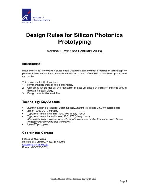
Design Rules for Silicon Photonics Prototyping - Institute of ...
Design Rules for Silicon Photonics Prototyping - Institute of ...
Design Rules for Silicon Photonics Prototyping - Institute of ...

You also want an ePaper? Increase the reach of your titles
YUMPU automatically turns print PDFs into web optimized ePapers that Google loves.
<strong>Design</strong> <strong>Rules</strong> <strong>for</strong> <strong>Silicon</strong> <strong>Photonics</strong><br />
<strong>Prototyping</strong><br />
Version 1 (released February 2008)<br />
Introduction<br />
IME’s <strong>Photonics</strong> <strong>Prototyping</strong> Service <strong>of</strong>fers 248nm lithography based fabrication technology <strong>for</strong><br />
passive <strong>Silicon</strong>-on-insulator photonic circuits at a cost af<strong>for</strong>dable to research groups and<br />
companies.<br />
This document briefly describes:<br />
1) Key fabrication process <strong>of</strong> this technology,<br />
2) Guidelines <strong>for</strong> the design and fabrication <strong>of</strong> passive <strong>Silicon</strong>-on-insulator photonic circuits<br />
through this technology,<br />
3) <strong>Design</strong> rules <strong>for</strong> the mask files.<br />
Technology Key Aspects<br />
• 200 mm <strong>Silicon</strong>-on-Insulator wafer: typically, 220nm top silicon, 2000nm buried oxide<br />
• 248nm deep UV lithography<br />
• Typical/minimum pitch [nm]: 450 / 400 (binary mask)<br />
• Typical/minimum line width [nm]: 220 / 170 (binary mask)<br />
(Phase Shift Mask is optional <strong>for</strong> structures with feature size smaller than above spec., Please<br />
contact coordinator <strong>for</strong> detailed in<strong>for</strong>mation.)<br />
• Use <strong>of</strong> Tip couplers<br />
Coordinator Contact<br />
Patrick Lo Guo Qiang<br />
<strong>Institute</strong> <strong>of</strong> Microelectronics, Singapore<br />
logq@ime.a-star.edu.sg<br />
Phone: +65-6770-5705<br />
Property <strong>of</strong> <strong>Institute</strong> <strong>of</strong> Microelectronics. Copyright © 2008<br />
Page 1
Contents<br />
1. Description <strong>of</strong> Key Fabrication Process<br />
1.1 Fabrication Process flow 3<br />
1.2 Wafer Specification 3<br />
1.3 Lithography 3<br />
1.4 Etching 4<br />
1.5 Mask Technology 4<br />
1.6 Facilitating Measurements 4<br />
2. <strong>Design</strong> <strong>Rules</strong><br />
2.1 Minimum Feature Sizes 5<br />
2.2 Multiple Structure <strong>Design</strong> 5<br />
2.3 Multiple Circuit <strong>Design</strong> 6<br />
2.4 Appendix: Exposure Latitude <strong>for</strong> Some Critical Structures 6<br />
Photonic Crystal Holes 6<br />
Isolated Lines (photonic wires) 7<br />
Gap Width 8<br />
Tip Coupler <strong>Design</strong> 8<br />
3. Mask File<br />
3.1 Mask File Format 9<br />
3.2 Hierarchy 9<br />
3.3 S<strong>of</strong>tware 9<br />
3.4 Dark Field/ Light Field 10<br />
3.5 Layer Structure 10<br />
3.6 General Layout Rule 11<br />
Property <strong>of</strong> <strong>Institute</strong> <strong>of</strong> Microelectronics. Copyright © 2008<br />
Page 2
1. Description <strong>of</strong> Key Fabrication Process<br />
1.1 Fabrication Process Flow<br />
The standard fabrication process flow IME uses <strong>for</strong> photonic passive device and<br />
components are schematically shown as below (here 248nm lithography is used):<br />
(a) Bare Si-substrate wafer<br />
Si<br />
-- Si-substrate<br />
SiO2<br />
-- Buried SiO 2 (2 μm)<br />
-- Top Si Layer (220nm)<br />
Si<br />
(b) Bottom AR coating (BARC)<br />
(c) Photo-resist (PR) coating and s<strong>of</strong>t bake<br />
(d) Exposure<br />
(e) Post-exposure bake<br />
(f) Development<br />
PR<br />
Si<br />
SiO2<br />
Si<br />
Barc<br />
(g) BARC & <strong>Silicon</strong> etch<br />
PR<br />
Si<br />
SiO2<br />
Barc<br />
Si<br />
(h) Photo-resist strip & clean<br />
(i)<br />
Si-surface Treatment<br />
Si<br />
SiO2<br />
Si<br />
1.2 Wafer Specification<br />
The wafers are <strong>Silicon</strong> on Insulator (SOI), typically with 220nm top silicon layer and<br />
2000nm buried oxide.<br />
1.3 Lithography<br />
The standard lithography process used <strong>for</strong> nanophotonic structures makes use <strong>of</strong> 410 nm<br />
thick Shipley UV210 resist with a bottom antireflective coating; exposed with illumination<br />
conditions <strong>of</strong> numerical aperture <strong>of</strong> 0.68 and a spatial coherency factor <strong>of</strong> 0.31.<br />
Property <strong>of</strong> <strong>Institute</strong> <strong>of</strong> Microelectronics. Copyright © 2008<br />
Page 3
1.4 Etching<br />
ICP low pressure/high density etch system with a chemistry based on SF 6 /C 4 F 8 /O 2 is used<br />
to etch only the top <strong>Silicon</strong> layer.<br />
Prior to hardmask and Si etching, BARC etch is per<strong>for</strong>med using plasma etching that also<br />
smoothen the sidewall <strong>of</strong> resist to reduce roughness (refer to process flow). BARC etch can<br />
also be used to compensate <strong>for</strong> a feature size bias between litho and etch.<br />
1.5 Mask Technology<br />
The mask will be a binary Chrome Mask (without Phase Shifting features). The default<br />
polarity <strong>of</strong> the masks are dark-field, which means that all features defined on the mask will<br />
be transparent and there<strong>for</strong>e etched away (refer to 3.4 Dark Field/ Light Field <strong>for</strong> details).<br />
The mask will have a useful area roughly 10 x 13.2 cm 2 , with a reduction factor <strong>of</strong> 4 ×.<br />
Mask shop will be appointed by IME.<br />
(For users who require Phase Shift Mask <strong>for</strong> special design, please contact coordinator <strong>for</strong> more<br />
in<strong>for</strong>mation.)<br />
1.6 Facilitating Measurements<br />
IME provides deep trench etch process using deep reactive ion etch (DRIE) to facilitate<br />
optical measurements, without additional ef<strong>for</strong>t <strong>of</strong> polishing after wafer dicing.<br />
IME also provides wafer dicing and packaging services.<br />
Please contact the technical coordinator <strong>for</strong> more in<strong>for</strong>mation:<br />
Patrick Lo Guo Qiang<br />
<strong>Institute</strong> <strong>of</strong> Microelectronics, Singapore<br />
logq@ime.a-star.edu.sg<br />
Phone: +65-6770-5705<br />
Property <strong>of</strong> <strong>Institute</strong> <strong>of</strong> Microelectronics. Copyright © 2008<br />
Page 4
2. <strong>Design</strong> <strong>Rules</strong><br />
2.1 Minimum Feature Sizes<br />
The minimum feature size that can be fabricated depends on the type <strong>of</strong> structure needed<br />
(i.e., dependent on pattern density, shapes etc). To provide some guidelines <strong>for</strong> design,<br />
the following table lists some <strong>of</strong> the minimum feature sizes that can be fabricated within a<br />
periodic pattern. For users with more complex design requirements, kindly contact the<br />
technical coordinator <strong>for</strong> more in<strong>for</strong>mation.<br />
Periodic structure Feature Minimum Size Typical Size<br />
Pitch > 400nm > 450nm<br />
Lines Width > 170nm > 220nm<br />
Line spacing > 180nm > 220nm<br />
Triangular Holes Diameter > 190nm > 220nm<br />
Triangular Holes Spacing > 200nm > 240nm<br />
For feature sizes smaller than the above listed specifications, resolution enhancement by use<br />
<strong>of</strong> Phase Shift Masking may be used. Kindly contact the coordinator <strong>for</strong> more in<strong>for</strong>mation.<br />
2.2 Multiple Structure <strong>Design</strong><br />
Fabricated feature size varies as a function <strong>of</strong> exposure dose, which is typically expressed<br />
in mJ/cm 2 ; quantifying the amount <strong>of</strong> light projected onto the photo-resist. E.g. holes will<br />
become larger <strong>for</strong> a higher exposure dose, while lines will become smaller. The dose used<br />
to fabricate structures at the desired size is called “best exposure dose”. However, in<br />
general, structures <strong>of</strong> different types (holes vs. lines) and even structures <strong>of</strong> the same type<br />
with different feature/pitch size will have different “best exposure dose”. There<strong>for</strong>e, one<br />
should take special care when incorporating structures <strong>of</strong> different types (e.g. photonic<br />
wires and photonic crystals) on a single mask design.<br />
Usually a sweep <strong>of</strong> the exposure dose is per<strong>for</strong>med to estimate the “best exposure dose” <strong>of</strong><br />
the most critical structure(s). The results are summarized in the Figures <strong>of</strong> 2.4 Appendix.<br />
Some mask design bias may be designed based on the data provided in these figures.<br />
The following example illustrates a possible mask design bias:<br />
Example 1: when incorporating a photonic crystal structure with triangular holes <strong>of</strong> diameter<br />
350nm and pitch <strong>of</strong> 500nm, together with an isolated line (photonic wire) <strong>of</strong> 500nm width on<br />
a single mask design, “best exposure dose” <strong>for</strong> holes is 40 mJ/cm 2 (see Figure 1 in 2.4<br />
Appendix). However, at this dose, the isolated line will print at 410nm width instead <strong>of</strong> the<br />
intended 500nm width, giving <strong>of</strong>f-target results (see Figure 3 in 2.4 Appendix).<br />
While it is most recommended that there should be only one critical structure on each layer,<br />
i.e. <strong>for</strong> instance in example 1, either the hole size <strong>of</strong> the photonic crystal structure or the<br />
width <strong>of</strong> the coupling wire should be critical; a ‘work-around’ solution to get both features to<br />
print on-target in this case would be to adjust one or more structures’ size in order that they<br />
print correctly at the same exposure dose. That is, in this case, the layout <strong>of</strong> the isolated<br />
line on the mask can be increased to 580nm (to give the necessary 80nm design bias), so<br />
that both photonic crystal structures and isolated line (photonic wire) can print correctly at<br />
the same exposure <strong>of</strong> 40 mJ/cm 2 .<br />
Property <strong>of</strong> <strong>Institute</strong> <strong>of</strong> Microelectronics. Copyright © 2008<br />
Page 5
In conclusion <strong>for</strong> this example, it should be noted that while such straight <strong>for</strong>ward design<br />
bias works well <strong>for</strong> simple structures, more complicated designs require more advance<br />
compensation techniques such as placement <strong>of</strong> scattering bars etc <strong>for</strong> design <strong>of</strong> mask<br />
biases. For such jobs, kindly contact the coordinator <strong>for</strong> more in<strong>for</strong>mation.<br />
2.3 Multiple Circuit <strong>Design</strong><br />
When incorporating multiple circuits with different “best exposure dose”, one can have all<br />
circuits on the same wafer, but on different dies if the various “best exposure dose”, are not<br />
too widely spread. Otherwise, different circuits will be fabricated on more than one wafer.<br />
2.4 Appendix<br />
Photonic Crystal Holes<br />
Figure 1 shows the measured diameter <strong>of</strong> holes patterned in a triangular hole array (on<br />
wafer) as a function <strong>of</strong> lithographic exposure dose <strong>for</strong> a variety <strong>of</strong> pitch and diameter (on<br />
mask).<br />
600<br />
Figure 1<br />
Triangular hole diameter vs Exposure dose<br />
Measured Hole Diameter [nm]<br />
500<br />
400<br />
300<br />
200<br />
100<br />
350:450<br />
<strong>Design</strong> diameter:pitch [nm]<br />
350:500<br />
300:500<br />
270:450<br />
240:400<br />
0<br />
20 30 40 50 60 70 8090100<br />
Exposure Dose [mJ/cm 2 ]<br />
Property <strong>of</strong> <strong>Institute</strong> <strong>of</strong> Microelectronics. Copyright © 2008<br />
Page 6
Figure 2 shows the measured diameter <strong>of</strong> holes patterned in square lattice array (on wafer)<br />
as a function <strong>of</strong> lithographic exposure dose <strong>for</strong> a variety <strong>of</strong> pitch and diameter (on mask).<br />
Figure 2<br />
Measured Hole Diameter [nm]<br />
500<br />
400<br />
300<br />
200<br />
100<br />
0<br />
Square hole diameter vs exposure dose<br />
<strong>Design</strong> diameter:pitch [nm]<br />
250:500<br />
226:450<br />
200:400<br />
20 30 40 50 60 70 8090100<br />
Exposure Dose [mJ/cm 2 ]<br />
Isolated Lines (Photonic Wires)<br />
Figure 3 shows the measured line width (on wafer) as a function <strong>of</strong> lithographic exposure<br />
dose <strong>for</strong> a variety <strong>of</strong> designed line widths (on mask)<br />
Figure 3<br />
800<br />
Isolated line width vs exposure dose<br />
Measured line width [nm]<br />
700<br />
600<br />
500<br />
400<br />
300<br />
200<br />
100<br />
200<br />
design iso-line width [nm]<br />
700<br />
600<br />
500<br />
400<br />
300<br />
0<br />
20 30 40 50 60<br />
Exposure dose [mJ/cm 2 ]<br />
Property <strong>of</strong> <strong>Institute</strong> <strong>of</strong> Microelectronics. Copyright © 2008<br />
Page 7
Gap Width<br />
Figure 4 shows the measured gap spacing (on wafer) between two lines with width <strong>of</strong> 0.3<br />
μm as a function <strong>of</strong> lithographic exposure dose <strong>for</strong> a variety <strong>of</strong> designed gap widths (on<br />
mask).<br />
.<br />
Measured Gap Width [nm]<br />
Tip Coupler<br />
900<br />
800<br />
700<br />
600<br />
500<br />
400<br />
300<br />
200<br />
100<br />
0<br />
Figure 4<br />
Gap width vs exposure dose<br />
design gap width [nm]<br />
600 nm<br />
550 nm<br />
500 nm<br />
450 nm<br />
400 nm<br />
350 nm<br />
300 nm<br />
250 nm<br />
200 nm<br />
20 30 40 50 60 70 80 90<br />
Exposure Dose [mJ/cm 2 ]<br />
For tip coupler, the following figure shows an example:<br />
a = 180 nm<br />
b = 200 µm<br />
Si waveguide<br />
a<br />
b<br />
Property <strong>of</strong> <strong>Institute</strong> <strong>of</strong> Microelectronics. Copyright © 2008<br />
Page 8
3. Mask Files<br />
3.1 File Format<br />
For submission <strong>of</strong> design layout to IME, the file <strong>for</strong>mat to be used should be GDSII. As not<br />
all s<strong>of</strong>tware tools support the full GDSII command set, users should limit structure<br />
definitions to the following types:<br />
i. BOUNDARY<br />
Filled, closed polygons; with a maximum <strong>of</strong> 200 nodes.<br />
ii. PATH<br />
Open lines with a physical width.<br />
iii. Simple Reference (SREF)<br />
Singular reference to a previously defined structure. Trans<strong>for</strong>mations on references are<br />
allowed as long as the rotation angle is a multiple <strong>of</strong> 90º.<br />
iv. Array Reference (AREF)<br />
An array <strong>of</strong> references to a previously defined structure. Trans<strong>for</strong>mations on references are<br />
allowed as long as the rotation angle is a multiple <strong>of</strong> 90º.<br />
Here, it is to be noted that the use <strong>of</strong> BOUNDARY type structures are preferred to PATH<br />
type in order to avoid arbitrary grid snapping in PATH type boundaries. Also, the following<br />
structure types are NOT supported:<br />
i. NODE<br />
Such elements are ignored and will not be fabricated on the mask.<br />
ii. LABEL<br />
Such elements are also ignored and will not appear on the mask.<br />
3.2 Hierarchy<br />
The layout should make full use <strong>of</strong> the GDSII hierarchy scheme such that SREFs and<br />
AREFs are used to define repeating structures where possible so as to keep final layout file<br />
size acceptably low. For instance, where a periodic photonic crystal lattice is required, it<br />
should not be composed <strong>of</strong> copying thousands <strong>of</strong> individual polygons, but rather created<br />
through instances call up <strong>of</strong> SREFs or AREFs.<br />
The final layout should comprise <strong>of</strong> only a single top cell in which the other sub-cells <strong>of</strong><br />
SREFs and AREFs lower on the hierarchy are referenced.<br />
3.3 S<strong>of</strong>tware<br />
GDSII layouts may be created on most layout tools such as Cadence, Silvaco Expert, L-edit<br />
etc. For partners without such s<strong>of</strong>tware, layout can be created by IME in-house at a fee.<br />
Alternatively, free layout s<strong>of</strong>tware such as Ruby GDSII Library may be used <strong>for</strong> writing<br />
GDSII data in the Ruby programming language (http://en.wikipedia.org/wiki/Ruby). As this<br />
is a third-party s<strong>of</strong>tware, its correctness and usage is solely the decision <strong>of</strong> the user, <strong>for</strong><br />
which IME cannot be responsible <strong>for</strong>.<br />
For viewing <strong>of</strong> GDSII files without data manipulation, the free s<strong>of</strong>tware CleWin may be used<br />
(http://www.phoenixbv.com ).<br />
Property <strong>of</strong> <strong>Institute</strong> <strong>of</strong> Microelectronics. Copyright © 2008<br />
Page 9
3.4 Dark Field/ Light Field<br />
For ease <strong>of</strong> definition, the default polarity <strong>of</strong> the masks are in dark field, so that structures<br />
defined in the layout mask files become transparent on a chrome background, and are<br />
etched away after processing. On the other hand, to accommodate layers whereby it is<br />
much simpler to define the structures as portions that should not be etched away (<strong>for</strong><br />
example in waveguides layers <strong>for</strong> lines features), light field layer definition may be used<br />
instead <strong>of</strong> laying out two trenches to define the line.<br />
For layers whereby there are to be both light and dark field features, the different fields are<br />
to be laid out on separate GDSII layer numbers so as to enable subsequent logic operation<br />
processing as shown in the next section. In general, it is highly recommended that each<br />
layer consist <strong>of</strong> a single field type (i.e., either light or dark field).<br />
3.5 Layer Structure<br />
To facilitate the processing <strong>of</strong> mask data and also the application <strong>of</strong> proximity corrections <strong>for</strong><br />
mask data optimization. A table <strong>of</strong> the different categories <strong>for</strong> structure types is listed as<br />
follows <strong>for</strong> layout drawing layer assignment:<br />
Layer<br />
Number<br />
Layer Type<br />
1 to 5 Non critical<br />
6 to 10 Typical<br />
11 to 15<br />
16 to 20<br />
21 to 25<br />
26 to 30<br />
31 to 35<br />
36 to 40<br />
Critical<br />
Alternating<br />
phase shifted<br />
Structure<br />
Lines, trenches,<br />
polygons etc<br />
Lines, trenches,<br />
polygons etc<br />
Lines<br />
Trenches<br />
Holes, pillars, polygon<br />
widest dimension<br />
Lines<br />
Trenches<br />
Holes Only<br />
Critical<br />
Dimension (CD)<br />
≥ 1 µm<br />
250 nm ≤ CD < 1 µm<br />
Examples<br />
Alignment marks, text,<br />
logos, fiber grooves etc<br />
Broad lines, ridges,<br />
polygons etc<br />
170 nm ≤ CD < 250 nm Photonic wires, tapers<br />
180 nm ≤ CD < 250 nm Gaps<br />
190 nm ≤ CD < 250 nm Photonic crystal lattice<br />
100 nm ≤ CD < 150 nm Waveguides, gratings<br />
140 nm ≤ CD < 190 nm Gratings, gaps<br />
160 nm ≤ CD < 200 nm Photonic crystal<br />
Here, the density <strong>of</strong> the patterns should also be specified, as a function <strong>of</strong> pitch, which<br />
should not be less than 400nm unless they are <strong>of</strong> the alternating phase shifted type, which<br />
has minimum pitch <strong>of</strong> 280nm <strong>for</strong> line space patterns and 300nm <strong>for</strong> hole-type feature.<br />
Also, <strong>for</strong> layers with more than one type <strong>of</strong> structure, the categorisation <strong>of</strong> layers is<br />
determined by the smallest feature on that mask. For example, <strong>for</strong> a mask having both<br />
photonic crystal structures (with CD <strong>of</strong> 250nm), together with broad line waveguides, the<br />
mask is assigned a layer number ranging from 21 to 25 <strong>for</strong> data processing.<br />
On a final note, further to the description <strong>for</strong> combining <strong>of</strong> clear and dark feature on a same<br />
mask. The following Figure 5 schematically explains the logical ‘OR’ operation <strong>of</strong> a dark<br />
field (photonic crystal layer ‘X’) with a clear field (waveguide layer ‘Y’) layout <strong>for</strong> final layout<br />
patterned structure as given in schematic ‘Z’.<br />
Property <strong>of</strong> <strong>Institute</strong> <strong>of</strong> Microelectronics. Copyright © 2008<br />
Page 10
Dark field -<br />
Photonic<br />
crystal drawn<br />
as squares<br />
Layout<br />
layer<br />
‘X’<br />
OR<br />
Clear field -<br />
Waveguides<br />
drawn as lines<br />
Layout<br />
layer<br />
‘Y’<br />
To obtain this<br />
final patterned<br />
structure<br />
Etched<br />
pattern<br />
on wafer<br />
White area =<br />
resist cleared<br />
Figure 5: Schematic <strong>of</strong> logical operation involving combination <strong>of</strong> both dark and clear field<br />
On a same mask layer.<br />
3.6 General Layout <strong>Rules</strong> <strong>for</strong> Basis Cells<br />
For mask fabrication at IME, all layout contributions will be fitted onto a basis cell size <strong>of</strong><br />
either 25 × 32 mm 2 or 25 × 16 mm 2 . This is to allow <strong>for</strong> standardised processing flow and<br />
optimised utilisation <strong>of</strong> mask area. For every mask layer which requires subsequent<br />
alignment and process quantification, clear-out areas without interference from other<br />
patterns need to be reserved <strong>for</strong> both alignment and metrology structures. In general, ‘N’<br />
such layers would require layout area <strong>of</strong> ‘N × 2500 × 100 μm 2 ’ horizontally and ‘N × 2100 ×<br />
100 μm 2 ’ vertically. Further, <strong>for</strong> every two layers with overlay requirement, clear-out area <strong>of</strong><br />
150 × 80 μm 2 need to be reserved at each corner <strong>of</strong> the basis cell.<br />
Property <strong>of</strong> <strong>Institute</strong> <strong>of</strong> Microelectronics. Copyright © 2008<br />
Page 11