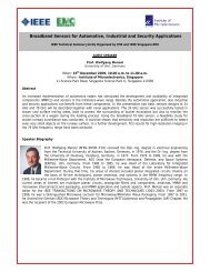
Si Stacked Module - Institute of Microelectronics - A*Star
Si Stacked Module - Institute of Microelectronics - A*Star
Si Stacked Module - Institute of Microelectronics - A*Star

You also want an ePaper? Increase the reach of your titles
YUMPU automatically turns print PDFs into web optimized ePapers that Google loves.
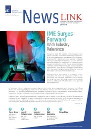
NEWSLINK<br />
A publication <strong>of</strong> the <strong>Institute</strong> <strong>of</strong> <strong>Microelectronics</strong><br />
ISSN 0218-7477<br />
An ISO 9001 certified organisation<br />
April 2004<br />
Contents<br />
2 Copper low-k<br />
interconnects<br />
and Packaging<br />
3 IME helping<br />
<strong>Si</strong>ngapore enterprises<br />
to “Grow, Glow, and<br />
4 to 5<br />
Globalise”<br />
New microlithography<br />
techniques for device<br />
miniaturization<br />
6 8 to<br />
News Bites<br />
<strong>Si</strong> <strong>Stacked</strong> <strong>Module</strong> - a platform technology<br />
for semiconductor integration<br />
and packaging<br />
<strong>Si</strong> stacked module: 11 chips on 3 camiers at 1.2mm total height.<br />
IME has developed a platform technology for silicon (<strong>Si</strong>)<br />
stacked module. The <strong>Si</strong> stacked module aims to combine<br />
different devices and circuit functions within the same<br />
module. The development <strong>of</strong> <strong>Si</strong> stacked module is timely in<br />
meeting the complex performance, cost, and size demands<br />
<strong>of</strong> portable electronic devices, high performance computing<br />
systems, and communication and entertainment systems,<br />
which run on various combinations <strong>of</strong> analog, digital, memory,<br />
signal processing, communications or optical ICs.<br />
4. <strong>Si</strong> micro-channeled liquid-cooled heat sink.<br />
The successful demonstration <strong>of</strong> <strong>Si</strong> stacked module has<br />
attracted 9 companies to join forces with IME on 30th<br />
January 2004 to develop the second generation <strong>of</strong> <strong>Si</strong> stacked<br />
module through IME’s flagship consortium - 7th Electronic<br />
Packaging Research Consortium (EPRC VII). For the first<br />
time, this EPRC VII is championed by IME and three other<br />
Comparing to conventional 2D integration and packaging,<br />
3D integration and packaging <strong>of</strong>fer advantages such as<br />
higher packaging density, lower interconnect loss & delay<br />
due to proximity between chips etc. To realize 3D integration<br />
and packaging, there are three methods <strong>of</strong> stacking, i.e. chip<br />
level, package level and wafer-level stacking.<br />
a<br />
b<br />
Combining the best <strong>of</strong> both chip level and wafer level stacking,<br />
IME <strong>Si</strong> stacked module <strong>of</strong>fers unique features such as<br />
1. Wafer level test strategy;<br />
2. High yield and thus overcoming the Known Good-Die<br />
(KGD) issue in 3D integration and packaging technologies;<br />
3. Low insertion loss <strong>of</strong> less than -0.5dB at 40GHz;<br />
4. Integrated cooling structure fabricated within the <strong>Si</strong><br />
stacked module up to 80W power dissipation.<br />
c<br />
(a) Through wafer solder interconnects, (b) Through wafer copper<br />
interconnects, (c) Ultra thin 8” wafer (d) Ultra thin bumped wafer<br />
d<br />
To make the <strong>Si</strong> stacked module possible, a full range <strong>of</strong> state<strong>of</strong>-the-art<br />
facilities, expertise and competencies are needed,<br />
including<br />
1. <strong>Si</strong> carrier processing;<br />
2. <strong>Si</strong> through wafer interconnect;<br />
3. Wafer thinning and handling solutions for MEMS wafers<br />
& bumped <strong>Si</strong> wafers with the latter’s thickness down to<br />
70 µm;<br />
Integrated<br />
cooling<br />
solution for<br />
<strong>Si</strong> stacked<br />
module.<br />
Continued to page 2 >><br />
A research institute <strong>of</strong> the Agency for Science, Technology and Research (A*STAR)
page 2<br />
Copper low-k interconnects and Packaging<br />
IME developed reliable Pb-free solder flip chip packaging for Cu/ultra low-k devices<br />
IC designers work to improve chip performance with more<br />
complex circuits and packing them even closer on a single<br />
piece <strong>of</strong> silicon. Limits are being reached as closely-packed<br />
circuits start to generate interference - just as crosstalk can<br />
occur between telephone lines. Traditionally, semiconductor<br />
industry has used aluminum as the conductor for “wiring”<br />
within the chip, and silicon-dioxide as dielectric for 30 years.<br />
However, the explosive demand for miniaturized and high<br />
performing electronics created the need for conductor<br />
material with higher electrical conductivity (i.e. copper), and<br />
other dielectric materials with lower k value.<br />
Notwithstanding these requirements, Copper low-k (Cu/lowk)<br />
technology has yet to be widespread in the IC industry<br />
because <strong>of</strong> processing and reliability issues such as delamination<br />
and bond pad failure. IME’s research efforts<br />
in these areas take the form <strong>of</strong> research consortia and<br />
collaborations with its industry partners.<br />
In 2001, COPBOND: Breakthrough in processing and wirebond<br />
packaging <strong>of</strong> Cu/low-k ICs<br />
IME’s Copper Chip Wire Bond Consortium (COPBOND), a<br />
14 member industrial consortium, achieved breakthrough<br />
in processing, packaging and testing ICs with Cu/low-k<br />
(k=2.67). Entering an un-chartered territory, this project<br />
successfully delivered technologies for packaging <strong>of</strong> Cu/<br />
low-k IC in standard Cu wire bonded BGA format. A novel<br />
wire bond fatigue methodology for reliability study was also<br />
established. IME’s expertise with extensive evaluations in<br />
structural modeling and bonding processes resulted in an<br />
innovative bond pad design. This enabled a reliable direct<br />
bonding <strong>of</strong> fine-pitch Cu wires onto the Cu/low-k structures.<br />
In this project different demonstrators <strong>of</strong> Cu/<strong>Si</strong>O2 & Cu/lowk<br />
chips with and without cap metallization were wire-bonded<br />
and packaged. They were all qualified under the industrial<br />
reliability standards.<br />
In 2002, WTC: Next significant milestone<br />
Striving towards addressing the next level <strong>of</strong> challenges,<br />
IME started <strong>Si</strong>ngapore’s first Wafer Technology Consortium<br />
(WTC) with 10 participating member companies in 2002.<br />
The consortium addressed challenges in flip chip packaging<br />
<strong>of</strong> Cu/ultra-low-k (ULK) devices (k=2.4). The team evaluated<br />
different stack structures in Cu/ultra-low-k devices. The<br />
leading research effort delivered new concepts for flip chip<br />
packaging solution which meet all industrial level reliability<br />
tests. For the first time in the world, a Cu-based under bump<br />
metallization which can be integrated into the Cu backend-<strong>of</strong>-line<br />
fabrication was developed for Pb-free solder<br />
bumping. With that, reliable flip-chip packaging for Cu/ultralow-k<br />
devices was established.<br />
Continued from 1 >><br />
sister institutes IMRE (<strong>Institute</strong> <strong>of</strong> Materials<br />
Research and Engineering), IHPC (<strong>Institute</strong> <strong>of</strong><br />
High Performance Computing) and SIMTech<br />
(<strong>Si</strong>ngapore <strong>Institute</strong> <strong>of</strong> Manufacturing<br />
Technology) under the umbrella <strong>of</strong> Micro-<br />
System Packaging (MSP) program (formerly<br />
known as Electronic Packaging or EP).<br />
<strong>Si</strong> stacked module is one <strong>of</strong> the many recent<br />
milestones that IME achieved in its <strong>Si</strong>-based<br />
advanced packaging program, which also<br />
includes<br />
1. Surface mountable 3D wafer level packaging<br />
for MEMS;<br />
2. Wafer level interconnects & packaging<br />
targeting at future ICs <strong>of</strong> 10,000 I/Os at<br />
20 µm pitch. In 2003, wafer level package<br />
(WLP) <strong>of</strong> 600 I/Os @ 400 µm pitch was<br />
delivered to the member companies <strong>of</strong> 6th<br />
Electronic Packaging Research Consortium<br />
(EPRC VI); in 2004, WLP <strong>of</strong> 4,000 I/Os @<br />
100 µm pitch was achieved.<br />
3. Cu/low-K interconnects & packaging<br />
Surface Mountable Wafer<br />
Level Packaging for MEMS<br />
Together with six industry partners, IME developed low cost yet reliable<br />
wafer level packaging that is directly mountable to PCB. This platform<br />
technology is suitable for RF or inertial MEMS (micro-electromechanical<br />
system) found in e.g. industrial and communication electronics. 3D<br />
integration is also possible with other electronic functions.<br />
Highlights <strong>of</strong> the surface<br />
mountable WLP for<br />
MEMS are<br />
• Ultra low insertion loss<br />
page 3<br />
2004 and beyond...<br />
Technology and industrial thrusts propelled IME to spearhead<br />
the third research consortium on Cu/low-k packaging through<br />
WTC 2. This consortium was launched on 12 March 2004<br />
with the participation <strong>of</strong> seven member companies. Having<br />
completed the extensive work in flip chip packaging <strong>of</strong> single<br />
damascene Cu/ultra-low-k structures, the WTC 2 aims to<br />
resolve the challenges <strong>of</strong> wire bond and flip chip packaging<br />
<strong>of</strong> multilayer dual damascene Cu with hybrid <strong>of</strong> CVD and<br />
spin-on deposited low-k. The project emphasizes on:<br />
• Design, modeling & fabrication <strong>of</strong> test vehicles*<br />
• Materials, assembly & process characterization<br />
• Direct Au wire bond on Cu metallization and on IME<br />
alteranate cap metallization**.<br />
• Novel packaging approach enabling low stress on Cu/<br />
low-k stack<br />
* Cu/low-k ICs usually suffer from chipping during<br />
mechanical dicing. IME has developed a low-cost<br />
methodology which prevents mechanical dicing<br />
from causing chipping to ICs.<br />
** The advantages <strong>of</strong> IME alternate cap materials for<br />
Cu metallized devices are<br />
- simpler chemical process;<br />
- no additional masks required;<br />
- good bond quality;<br />
- better longevity to oxidation & corrosion<br />
compared to other capping methods, and<br />
- lesser probe pad damage compared to<br />
conventional aluminum cap.<br />
Alternate<br />
cap<br />
Tantalum<br />
barrier<br />
Au ball<br />
Cu bond pad<br />
Au ball<br />
<strong>Si</strong>licon<br />
Alternate cap metallization on Cu/low-k<br />
The first Wafer Technology Consortium (WTC 1) completed<br />
with excellent physical and electrical performance obtained<br />
from single damascene Cu/ultra-low-k interconnects<br />
(k=2.4) Cu metallization was successfully integrated for BEOL<br />
interconnection. The integrated Cu/dielectric metallization<br />
was also proven to be reliable.<br />
Other important results were obtained:<br />
• No integration issues such as voiding in ULK were<br />
observed;<br />
• Optimized etch and clean recipes produced straight trench<br />
pr<strong>of</strong>iles without carbon depletion;<br />
• Cu CMP recipe was successfully developed with 1.5psi<br />
down force without any peeling between metallization<br />
layer and dielectrics;<br />
• Dielectric liners improved CMP process margin and<br />
reliability performance.<br />
Supporting <strong>Si</strong>ngapore enterprises to<br />
“Grow, Glow, and Globalise”<br />
Growing Enterprises with Technology<br />
Upgrade, or GET-UP, is a pro-active<br />
integrated programme aimed at<br />
boosting the global competitiveness <strong>of</strong><br />
local technology-intensive enterprises<br />
to equip them for the knowledgebased<br />
economy. The programme<br />
harnesses the existing schemes <strong>of</strong><br />
EDB, SPRING <strong>Si</strong>ngapore, IE <strong>Si</strong>ngapore<br />
and the technical capabilities <strong>of</strong><br />
Agency for Science, Technology and<br />
Research (A*STAR) research institutes<br />
to assist these growing enterprises<br />
(GEs) upgrade & globalise.<br />
One <strong>of</strong> the key features <strong>of</strong> the GET-<br />
UP programme is the Technology<br />
for Enterprise Capability Upgrading<br />
“<br />
The researchers<br />
are a big boost to<br />
getting the new chip<br />
to market faster<br />
as the researchers<br />
have both commercial<br />
and technical<br />
expertise.<br />
Pang Tuck Wing ”<br />
CFO, WinEdge & Wireless<br />
(T-UP) scheme, in which highly skilled<br />
research engineers or scientists from<br />
the A*STAR research institutes are<br />
seconded to work full time in the<br />
participating local enterprise. The aim<br />
<strong>of</strong> the T-UP scheme is to upgrade the<br />
technology and competencies <strong>of</strong> local<br />
enterprises.<br />
IME is one <strong>of</strong> the seven research<br />
institutes participating in this scheme.<br />
To date, IME has seconded its research<br />
staff to FTD Technologies, WinEdge &<br />
Wireless, Intelligent Micro Devices<br />
(IMD), Inscope Labs, and AdvanPack<br />
Solutions.<br />
Continued to page 3 >>
page 4<br />
Continued from 3 >><br />
In the case <strong>of</strong> FTD Technologies, an<br />
IC design company, IME’s Dr Rajinder<br />
<strong>Si</strong>ngh is serving his attachment to<br />
FTD as its Chief Technology Officer.<br />
According to FTD Technologies: “Dr<br />
Rajinder is a role model to FTD’s<br />
technical team by his immense<br />
contribution to process and quality<br />
aspects. He is an important guide<br />
and benchmark who has helped FTD<br />
with new technology initiatives and<br />
is helping FTD to set new standards<br />
internally as well as make us more<br />
competitive in the technology world.<br />
... We do not know how we can<br />
operate without Rajinder in the future.<br />
In a quick time, he has become one <strong>of</strong><br />
the most valuable asset and value to<br />
the FTD group <strong>of</strong> companies and its’<br />
businesses.”<br />
For WinEdge & Wireless, IME’s<br />
seconded researchers M. K. Raja, Dr<br />
Yadav Ram Chandra, and Technical<br />
Advisor D. Pinjala enabled the<br />
company research into innovative<br />
ideas that were previously not<br />
possible. Mr Pang Tuck Wing, CFO<br />
<strong>of</strong> WinEdge & Wireless, said: “With<br />
this new improved R&D environment<br />
where there is a more vibrant R&D<br />
effort and projects, we could now<br />
have a more holistic approach to the<br />
development <strong>of</strong> the final products.<br />
This new R&D atmosphere has already<br />
generated some positive results in<br />
our UltraSST chipset solutions where<br />
the holistic approach has made the<br />
solutions more robust.<br />
From the results <strong>of</strong> our first T-Up<br />
project, which is the development <strong>of</strong><br />
the UltraSST phone application, our<br />
company has proceeded with the<br />
Project Jupiter where we have aimed<br />
to innovate a whole new radio system<br />
that is truly low-cost, good powerefficiency,<br />
and provides a robust<br />
wireless communication solution.”<br />
New microlithography<br />
techniques for device<br />
miniaturization<br />
New enabling technology for making 15nm FinFET device,<br />
100nm trenches and 140 nm vias for back-end-<strong>of</strong>-line<br />
(BEOL) Cu interconnects, and mass producible photonic<br />
crystal devices.<br />
In a bid to satisfy industry demands for smaller, more complex, and cost-efficient<br />
devices, IME researchers are working on new microlithography techniques to<br />
stretch their process technologies to capabilities beyond their limitations.<br />
Novel microlithography techniques for processing silicon wafers were developed<br />
using 248nm scanner. These techniques include Chromeless phase lithography<br />
(CPL), Alternating Phase Shift Mask (PSM), Attenuated PSM technology, and IME’s<br />
very own Dual Exposure With Shift (DEWS) method. These techniques are being<br />
implemented for patterning geometries for sub 130nm technology. Patterning is<br />
being developed for CMOS transistor gates, interconnect trenches and vias, and<br />
photonic crystals.<br />
In microlithography, either optical lithography or E-Beam is used. Optical<br />
lithography is the preferred process because it is faster, has a shorter printing time,<br />
and enables large-scale processing <strong>of</strong> large wafers.<br />
IME’s capabilities in microlithography<br />
Synergized capabilities to develop patterning technology for 90 nm node using<br />
Phase Shift Mask<br />
Together with Hoya Corporation, Japan, IME developed patterning technology<br />
for 90 nm and smaller technology node. The joint development program (JDP) is<br />
geared towards stretching the limits <strong>of</strong> the 248 nm exposure tool to pattern 90nm<br />
geometries for production. This JDP also aims at patterning geometries below 90<br />
nm for research purposes.<br />
The designs <strong>of</strong> phase shift masks are being<br />
done at IME using their in-house expertise.<br />
Valuable learning cycles are being used to<br />
identify the limits <strong>of</strong> different phase shift<br />
technologies, understand the positive and<br />
negative points <strong>of</strong> each technique, the<br />
limitations <strong>of</strong> mask making processes and<br />
improvements <strong>of</strong> the same.<br />
One <strong>of</strong> IME’s missions is to support<br />
the electronics industry in <strong>Si</strong>ngapore.<br />
We expect more <strong>of</strong> our researchers<br />
would be seconded to the industry in<br />
the coming months, thereby fulfilling<br />
our mission.<br />
Some examples <strong>of</strong> different techniques<br />
that are being used to pattern different<br />
structures will be discussed in the<br />
subsequent sections.<br />
15nm fin after patterning using<br />
CPL followed by resist trim
page 5<br />
Chromeless phase lithography<br />
Chromeless phase lithography (CPL) has enabled the<br />
patterning <strong>of</strong> 40nm fins for FinFET devices, which are 3D<br />
MOS transistors. The Fin Field Effect Transistor (FinFET) is<br />
a promising future CMOS device to control short channel<br />
effects and enhance drive current. The superior leakage<br />
control characteristics make FinFET transistors an attractive<br />
candidate for future nano-scale CMOS generations, which<br />
are expected to be in manufacturing within the next decade.<br />
With proper reticle design and adjustment <strong>of</strong> exposure dose<br />
conditions, the chromeless phase-shift technology leads 248<br />
nm scanner well below the resolution limit to pattern the 40<br />
nm thin fins for FinFET devices. After an effective resist trim<br />
process this size can be further reduced to 15 nm.<br />
IME’s fin patterning process provides inherent widening <strong>of</strong><br />
the Source/Drain (S/D) extension region, which is crucial in<br />
reducing the parasitic S/D resistance.<br />
CPL techniques have also been used for patterning<br />
conventional transistor structures. Promise is seen at<br />
patterning down to 90 nm gate structures.<br />
Alternating phase technology<br />
IME researchers have also developed technologies that use<br />
the conventional alternating phase method to pattern lines,<br />
trenches and holes for BEOL Cu interconnects. Both isolated<br />
and dense patterns for lines, trenches and holes have been<br />
realized in practice. Various optical techniques including<br />
the use <strong>of</strong> scatter bars have been used to pattern isolated<br />
trenches down to 100 nm and below.<br />
70 nm line 120 nm trench 88 nm trench<br />
Via size 140, 1:1 Pitch,<br />
Alternating Mask<br />
Via size 144 nm,<br />
1:5 Pitch<br />
140nm via at (a) higher density <strong>of</strong> 1:1 pitch and (b) lesser<br />
density <strong>of</strong> 1:4 pitch using alternating phase shift mask.<br />
88.3nm<br />
Via<br />
<strong>Si</strong>de<br />
lobe<br />
With side lobes<br />
Attenuated PSM Technology<br />
An effective method with anti side lobe structures have been<br />
put in place by IME to eliminate the appearance <strong>of</strong> sidelobes<br />
on an attenuated PSM.<br />
<strong>Si</strong>delobes are undesired patterns printed on wafers when<br />
attenuated (leaky chrome) masks are used for patterning.<br />
These are caused by negative field amplitude that is large<br />
with attenuated phase shift masks.<br />
A corrective lithography technology, attenuated PSM<br />
improves the edge contrast <strong>of</strong> features on advanced<br />
integrated circuits (ICs). This method can be used for<br />
structures <strong>of</strong> any size and shape, and replaces the more<br />
conventional method <strong>of</strong> using tri-tone masks (much higher<br />
cost), or manipulating undesirable design rules.<br />
DEWS technique for patterning sub-100nm lines<br />
What can normally be achieved by using only the most<br />
advanced and expensive Resolution Enhancement<br />
Techniques, high numerical apertures (NA>
NEWS BITES<br />
page 6<br />
Continued from 5>><br />
Volume production <strong>of</strong> ‘high<br />
fill factor’ photonic crystal<br />
devices a reality with 248 nm<br />
Lithography<br />
The use <strong>of</strong> photonic crystal to<br />
manipulate light in sub micrometer<br />
dimensions is a new approach. The<br />
abilities to manipulate lights such<br />
as guiding and trapping have many<br />
potential applications in optical<br />
communications and optical quantum<br />
computing. In this case, the optical<br />
lithography process (248nm scanner)<br />
is used to realize photonic crystals on<br />
silicon devices.<br />
IME and Toppan Electronics<br />
<strong>Si</strong>ngapore develop RFID chip<br />
IME, I 2 R, and Toppan join hands in the development <strong>of</strong> the RFID system<br />
IME has jointly developed an original 2.45GHz radio frequency identification (RFID)<br />
chip, TesStar (trademark pending) with Toppan Electronics <strong>Si</strong>ngapore (TES).<br />
Optical splitter on photonics crystals<br />
(100nm spacing between holes)<br />
Almost all research efforts in photonics<br />
crystals are currently at university<br />
labs, and E-beam lithography is<br />
widely used to pattern the photonic<br />
crystals. Due to inherently long<br />
writing times associated with e-bean<br />
lithography, optical lithography<br />
is preferred, if only the desired<br />
pattern dimensions can be achieved.<br />
IME’s efforts in using the 248 nm<br />
lithography for making photonic<br />
crystal structures is aimed to achieve<br />
this. Research efforts at IME focus<br />
on issues such as patterning square<br />
and triangular lattice arrangement<br />
<strong>of</strong> photonic crystals, proximity effect,<br />
and patterning line/space and hole<br />
together. As the pursuit includes<br />
patterning smaller periodicity <strong>of</strong><br />
structures, photonic crystals can be<br />
made for visible spectrum rather than<br />
the more common infrared.<br />
This small and complex CMOS-based chip consists <strong>of</strong> radio frequency, analog,<br />
and digital circuits together with efficient power generation circuits, has been<br />
optimized for maximum communication distance. Through this collaboration,<br />
new integrated circuit design<br />
intellectual properties were<br />
TesStar<br />
Antenna<br />
created.<br />
This development was announced<br />
in a joint press conference by<br />
Toppan, IME, and the <strong>Institute</strong><br />
<strong>of</strong> Infocomm Research (I 2 R), who<br />
Pr<strong>of</strong> Er and Dr Tan sealing the<br />
collaborative research effort between<br />
NTU and IME.<br />
RFID tags<br />
RFID<br />
tag<br />
Forging closer ties with university<br />
through Joint <strong>Microelectronics</strong><br />
Laboratory (JML)<br />
IME and the Nanyang Technological University<br />
(NTU) signed a memorandum <strong>of</strong> understanding<br />
to synergize their capabilities in the area<br />
<strong>of</strong> microelectronics. Three programs were<br />
identified for collaboration: <strong>Si</strong> micro-photonics;<br />
Micro and nano devices and technologies; and<br />
very high speed integrated circuit for optical<br />
and wireless communication. IME and National<br />
University <strong>of</strong> <strong>Si</strong>ngapore (NUS) also have a JML<br />
which is operational since 2003.<br />
This MOU will further enhance IME’s and NTU’s<br />
research efforts in microelectronics in the<br />
future.
page 7<br />
International recognitions<br />
Prized images in failure analysis<br />
wins international recognition<br />
IME’s Scanning Capacitance Micro-scopy<br />
(SCM) imaging <strong>of</strong> a 0.8µm n-channel transistor<br />
won the first prize in the 2003 International<br />
Symposium for Testing and Failure Analysis<br />
(ISTFA) conference. This image later went on<br />
to grace the cover <strong>of</strong> the Electronic Device<br />
Failure Analysis Society (EDFAS) Newsletter in<br />
February 2004.<br />
Different colors represent different material types: purple/pink N, red P, green/<br />
black oxide and heavily doped material.<br />
This is not the first time that IME’s<br />
research work has won an award. In<br />
2002, the SEM micrograph <strong>of</strong> our 8 layer<br />
metal interconnect structure <strong>of</strong> Cu dual<br />
damascene garnered the third prize at<br />
the ISTFA Photocontest, and was selected<br />
as the hero picture in the ISTFA 2003<br />
proceedings (right).<br />
IME researcher authored Ultra Large Scale Integration<br />
(ULSI) atlas<br />
Led by two IME staff, Chih-Hang Tung and George T.T. Sheng (retired from IME<br />
in 2000), this atlas was written by three renowned pioneers in their field. This<br />
is the first book available on the subject using fully TEM (Transmission Electron<br />
Microscopy) images. ULSI Semiconductor Technology Atlas uses examples and<br />
TEM micrographs to explain ULSI process technologies and their associated<br />
problems. More than 1,100 TEM images illustrate the science <strong>of</strong> ULSI.<br />
Dr Lim Thiam Beng, Deputy Director for Industry,<br />
received the IEEE CMPT Outstanding Sustained<br />
Technical Contributions Award<br />
For leading edge research in advanced packaging technologies and<br />
for managing and transferring that research and development to the<br />
microelectronics industry and research organisations worldwide.
NEWS BITES<br />
page 8<br />
Science Outreach program and Graduate<br />
Student Training<br />
Bringing microelectronics closer to<br />
<strong>Si</strong>ngapore youths<br />
In staging a series <strong>of</strong> events in conjunction with Science<br />
‘03 orangised by A*STAR, IME played an important role<br />
in educating <strong>Si</strong>ngapore’s youth by lending its expertise<br />
in microelectronics to the public event. The Science ‘03<br />
aimed to create greater awareness <strong>of</strong> science, technology<br />
and biomedicine, and to inspire and inculcate an interest in<br />
<strong>Si</strong>ngapore youths to pursue science as a career.<br />
Setting a precedent in the Science Outreach program<br />
history, a group <strong>of</strong> students from three secondary schools:<br />
River Valley High School, ShuQun Secondary School, and<br />
Clementi Town Secondary School learnt the basic knowledge<br />
<strong>of</strong> microelectronics from IME researchers and went ahead to<br />
build three creative science exhibits explaining some <strong>of</strong> the<br />
scientific and technical principles that go into the making<br />
<strong>of</strong> silicon chips. The students went further to explain the<br />
concepts <strong>of</strong> the exhibits in a public exhibition, and to their<br />
peers during an IME open house to students.<br />
Symposium <strong>of</strong> <strong>Microelectronics</strong> (SOM<br />
2003) enables young microelectronics<br />
aspirants to share research ideas<br />
As part <strong>of</strong> IME’s graduate student training program, this<br />
inaugural one day symposium created a new platform for<br />
research students attached to IME to present their research<br />
activities in microelectronics and to network with their<br />
peers.<br />
Students explaining the principles & concepts <strong>of</strong> their projects to<br />
their peers at the IME open house, another IME initiative to spark<br />
interest in microelectronics among youths.<br />
Owing to the overwhelming response and interest from the<br />
research students and university pr<strong>of</strong>essors, the symposium<br />
will now be an annual event. The SOM 2004 is scheduled for<br />
4th June 2004 and is currently calling for papers. For more<br />
information, visit www.ime.a-star.edu.sg<br />
IME innovations commercialized by<br />
local enterprise<br />
<strong>Si</strong>MEMS, a local company, signed a licensing agreement to utilize a special silicon-based<br />
micro-PCR and DNA micro extraction chip technologies. These two technologies were<br />
jointly developed by IME and the National University <strong>of</strong> <strong>Si</strong>ngapore through the Biosensor<br />
Focused Interest Group (BFIG).<br />
These two technologies will give <strong>Si</strong>MEMS a head-start in bringing their products closer to<br />
the market.<br />
Editorial Board<br />
Advisor: Lim Thiam Beng<br />
Editors: Janet Chang, Teo Keng Hwa<br />
Contributors: Mukherjee-Roy Moitreyee, V. Kripesh, Tsang Chi Fo, Mohandass <strong>Si</strong>vakumar