Untitled - IAP/TU Wien - Technische Universität Wien
Untitled - IAP/TU Wien - Technische Universität Wien
Untitled - IAP/TU Wien - Technische Universität Wien

You also want an ePaper? Increase the reach of your titles
YUMPU automatically turns print PDFs into web optimized ePapers that Google loves.
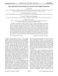
Nanostructure Characterisation by Electron Beam Techniques<br />
Experimental Effective Attenuation Length for applications in Hard X-ray<br />
photoelectron spectroscopy<br />
Juan Rubio-Zuazo, 1,2 and Germán R. Castro, 1,2,*<br />
1 SpLine Spanish CRG BM25 Beamline at the ESRF ESRF-BP 220-38043 Grenoble Cedex, France<br />
2 Instituto de Ciencia de Materiales de Madrid-ICMM/CSIC ; Cantoblanco, E-28049 Madrid, Spain<br />
*castro@esrf.fr<br />
Nowadays, the great challenge in materials science is the incorporation of complex systems in the<br />
area of the nano-technologies. Material composites, which combine different materials mostly multilayer thin<br />
films, with specific and defined properties, are a promising way to create products with specific properties.<br />
The photoemission and the Auger electron spectroscopies play a preponderant role in the study of the<br />
electronic properties of matter. Third generation synchrotron radiation sources enables the extension of XPS<br />
to higher electron kinetic energies (HAXPES, Hard X-ray PhotoElectron Spectroscopy) compensating the<br />
decrease of the photoionization cross-section for excitation energies in the hard X-ray region. HAXPES<br />
allows the accessibility to buried interfaces and bulk materials due to the dramatic increase of the effective<br />
attenuation length (EAL). Electronic, compositional and chemical depth profiles can be then performed in a<br />
non-destructive way over the tens-of nanometers scale with nanometer depth resolution. Such an important<br />
application of HAXPES is crucial for many condensed matter experiments and requires reliable EALs for<br />
high kinetic energy. EALs are well established for electrons with kinetic energies up to 2 keV. Even if EALs<br />
can be obtained by extrapolating well-known formulae, there is a lack of experimental data in the energy<br />
range between 1 and 15 keV, necessary to validate (or not) the proposed formulae. In the present study we<br />
have determined the EAL dependency on kinetic energy for titanium nitride (TiN), hafnium oxide (HfO 2 ),<br />
silicon (Si), silicon dioxide (SiO 2 ), lanthanum lutetium oxide (LaLuO 3 ), lanthanum calcium manganite<br />
(La 0.66 Ca 0.33 MnO 3 ), and gold (Au) from 1 keV up to 15 keV. A correlation between the EAL energy<br />
dependence and the material density is established. The EALs has been obtained by following either core<br />
level peak intensity dependence for a fixed kinetic energy as a function of the overlayer thickness or the core<br />
level peak intensity dependence with the photoelectron kinetic energy (i.e. photon energy) for a fixed<br />
overlayer thickness. The experimental set-up used is devoted to the combination of X-ray Diffraction (XRD)<br />
and HAXPES. Hence, we are able to determine the exact thickness and roughness of the layer from a fit of<br />
the X-ray reflectivity (Kiessig fringes) and simultaneously to obtain the EALs from the HAXPES signal<br />
evolution. It is important to stress that due to the simultaneous detection of the diffracted and photoemitted<br />
signal, the EALs, thickness and roughness determination correspond exactly to the same sample region.<br />
52