Untitled - IAP/TU Wien - Technische Universität Wien
Untitled - IAP/TU Wien - Technische Universität Wien
Untitled - IAP/TU Wien - Technische Universität Wien

You also want an ePaper? Increase the reach of your titles
YUMPU automatically turns print PDFs into web optimized ePapers that Google loves.
71st IUVSTA Workshop<br />
Mapping the surface structural and electronic properties of individual<br />
nanoparticles with the tiny beam of a Scanning Transmission Electron<br />
Microscope (STEM)<br />
Christian Colliex<br />
Laboratoire de Physique des Solides (UMR CNRS 8502)<br />
Bldg. 510, Université Paris-Sud 11, 91405 Orsay, France<br />
christian.colliex@u-psud.fr<br />
Aberration-corrected scanning transmission electron microscopes deliver Angström-sized<br />
electron probes of typically 40 to 200 kV kinetic energy, on individual nanoparticles, outside of them,<br />
on the apex of one of their external surfaces or through them. They constitute very powerful tools to<br />
investigate both the structural and electronic properties of the selected targets at the finest spatial<br />
resolution. As a result of the strong interactions between probe and matter, many different signals can<br />
be picked simultaneously (see figure below). Electrons scattered at large angles are collected by<br />
annular detectors and they deliver signals which are of use for reconstructing, atom by atom, the 3D<br />
structure of individual nanocrystals. In parallel, electron energy-loss spectroscopy (EELS) records the<br />
electronic excitation spectrum of the specimen over a very broad domain, typically from 1 to 1000 eV,<br />
with a high level of spatial and energy resolution. When using the core-loss signals, single atom<br />
sensitivity has been demonstrated and elemental maps, atomic column by atomic column, of<br />
crystallized nanoparticles or across interfaces, are now routinely available. In some cases, taking<br />
benefit of the fine structures appearing on the characteristic edges, the bonding state of the atoms<br />
across nanostructures and at their surfaces is also accessible. In the 1 to 5 eV range encompassing the<br />
visible spectral domain, one maps the distribution in energy and in intensity of the surface plasmon<br />
modes at metal surfaces with a spatial resolution typically down to 1 nm and an energy resolution of<br />
100 meV. It thus constitutes a very efficient technique to explore the sub-wavelength spatial variation<br />
of the electro-magnetic fields associated to surface plasmons. This is therefore a powerful alternative<br />
to near-field optical microscopy, with much increased spatial resolution, for investigating a broad<br />
range of photonic modes in very diversified geometries. Quite recently, spectrum-imaging of the<br />
emitted photons under the primary electron beam and the spectacular introduction of time-resolved<br />
techniques down to the fs-time domain, have constituted innovative keys for the development and use<br />
of a brand new multi-dimensional and multi-signal electron microscopy.<br />
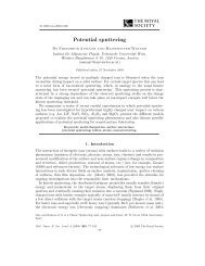
Illustration of the multisignal strategy in a<br />
modern STEM instrument, displaying two<br />
channels of parallel information : ADF, EELS<br />
and EDX elemental mapping of the atomic<br />
structure and composition in SrTiO3 (left) ;<br />
ADF, EELS plasmon map and cathodeluminescence<br />
(CL = photon emission<br />
spectroscopy) on a single Ag nanoplatelet<br />
(right)<br />
47