Untitled - IAP/TU Wien - Technische Universität Wien
Untitled - IAP/TU Wien - Technische Universität Wien
Untitled - IAP/TU Wien - Technische Universität Wien

Create successful ePaper yourself
Turn your PDF publications into a flip-book with our unique Google optimized e-Paper software.
71st IUVSTA Workshop<br />
Modeling Scanning Electron Microscope Measurements with Charging<br />
J. S. Villarrubia *<br />
National Institute of Standards and Technology, Gaithersburg, MD 20899, USA<br />
* John.Villarrubia@nist.gov<br />
Nanostructured samples that are relevant in semiconductor electronics manufacturing or in nanotechnology<br />
are often comprised of mixed materials, some of which are insulators. Accumulated charges in insulating<br />
regions exposed to the electron beam or to scattered electrons generate electric fields that alter the contrast<br />
and positions of features in acquired images. To interpret the images it is necessary to account for these effects.<br />
For this purpose, the existing<br />
JMONSEL [1,2] simulator has been<br />
augmented with charging-related modeling<br />
capabilities. JMONSEL already<br />
performed Monte Carlo scattering simulations<br />
that included elastic scattering<br />
via the Mott cross sections, inelastic<br />
scattering via the dielectric function<br />
theory approach (when the requisite<br />
material data are available), phonon<br />
scattering, and electron refraction at<br />
material boundary crossings. For simulations<br />
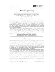
in which charging is important, the sample is represented as a tetrahedral mesh with variable mesh size:<br />
fine in the region of interest and increasingly coarse with distance (Fig. 1). The net charge due to trapped electrons<br />
or holes in each mesh element is tracked. Simulation proceeds iteratively in a cycle that includes finite<br />
element solution of the electric fields followed by a scattering phase with electron transport modified by the<br />
electric field.<br />
The new capabilities have been used to simulate imaging of unfilled contact holes with radius 35 nm to<br />
70 nm through SiO 2 (Fig. 1) with a view to determining the dependence of visibility of the hole bottom upon<br />
hole size and imaging conditions. Results indicate that under appropriate conditions, the SiO 2 develops a beneficial<br />
positive surface potential that saturates at a scan-size dependent amount. This potential helps to extract<br />
electrons from the hole bottom.<br />
Fig. 1. Cutaway of meshed contact hole and surrounding volume. Tetrahedra<br />
that intersect a plane through the axis of the hole are rendered as solids.<br />
Oxide is blue, the vacuum above the hole is green, and (inset) the vacuum in<br />
the hole itself is purple.<br />
References<br />
[1]J. S. Villarrubia, N. W. M. Ritchie, and J. R. Lowney, Proc. SPIE 6518 (2007) 65180K.<br />
[2]J. S. Villarrubia and Z. J. Ding, J. Micro/Nanolith. MEMS MOEMS 8 (2009) 033003.<br />
25