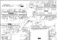
PC BOARD (Component side view)
PC BOARD (Component side view)
PC BOARD (Component side view)

Create successful ePaper yourself
Turn your PDF publications into a flip-book with our unique Google optimized e-Paper software.
RXD-V525/V626/V727/V828<br />
10<br />
CD player adjustment<br />
NO. ITEM<br />
INPUT<br />
SETTINGS<br />
ADJUSTMENT<br />
OUTPUT<br />
SETTINGS<br />
CD PLAYER<br />
SETTINGS<br />
ALIGNMENT ALIGN FOR FIG.<br />
NO. [1] :Choose either LASER POWER or LASER CURRENT CHECK. ( Confirm to be satisfied either LASER POWER or LASER<br />
CURRENT CHECK.)<br />
TEST MODE : While pressing the PLAY/PAUSE key ,plug the power code into the AC power wall output.<br />
Insert TEST DISC.<br />
[1]<br />
[1]<br />
[2]<br />
LASER<br />
POWER<br />
LASER CURRENT<br />
CHECK<br />
-<br />
Test disc<br />
type4<br />
Set the sensor<br />
section of the<br />
optical power meter<br />
on the pickup lens.<br />
Set the tester<br />
between both the<br />
check land of R8 (10<br />
‰) on the <strong>PC</strong>B(X32)<br />
of the set upper.<br />
Press the<br />
PLAY/PAUSE key to<br />
check that the display<br />
is "03".<br />
Press the<br />
PLAY/PAUSE key to<br />
check that the display<br />
is "03" or "05".<br />
(Caution) Connect and remove to the tester for the laser current check at POWER OFF condition.<br />
FOCUS ERROR<br />
BIAS<br />
Test disc<br />
type4<br />
Connect an<br />
oscilloscope as<br />
follows.<br />
CH1:RF(CN1:1pin)<br />
GND:VC(CN1:4pin)<br />
(Note) Type 4 disc: SONY YEDS-18 test disc or equivalent. (KTD-02)<br />
Press the<br />
PLAY/PAUSE key .<br />
Confirm that the<br />
display is "05".<br />
(a) Laser Power (b) Test point<br />
(d)<br />
Pickup<br />
RF signal: AC coupled<br />
0.05~0.15 mW<br />
Optical power meter<br />
• RF signal in test mode (PLAY).<br />
• Perform the tangential and focusing offset are<br />
focused into one point on the display. The crossing<br />
points above and below the center shall also be<br />
looked clearly.<br />
CN2<br />
NC<br />
TE1<br />
TE2<br />
VC CN1<br />
FE2<br />
FE1<br />
RF<br />
VR1<br />
Q1<br />
R8<br />
-<br />
On the power from 0.05<br />
to 0.15mW.When the<br />
diffraction grating is<br />
correctly aligned with<br />
the RF level of 0.8Vp-p<br />
or more.<br />
- 500–200mV<br />
FE BIAS<br />
VR1<br />
FRONT<br />
(a)<br />
Optimum eye pattern (b) (d)<br />
X32<br />
(<strong>Component</strong> <strong>side</strong>)