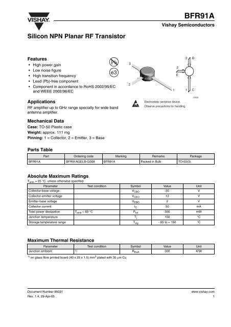
BFR91A
BFR91A
BFR91A

You also want an ePaper? Increase the reach of your titles
YUMPU automatically turns print PDFs into web optimized ePapers that Google loves.
<strong>BFR91A</strong><br />
Vishay Semiconductors<br />
Silicon NPN Planar RF Transistor<br />
Features<br />
• High power gain<br />
• Low noise figure<br />
• High transition frequency<br />
• Lead (Pb)-free component<br />
• Component in accordance to RoHS 2002/95/EC<br />
and WEEE 2002/96/EC<br />
e3<br />
3<br />
2<br />
1<br />
2<br />
E<br />
3<br />
1<br />
B<br />
C<br />
Applications<br />
RF amplifier up to GHz range specially for wide band<br />
antenna amplifier.<br />
Electrostatic sensitive device.<br />
Observe precautions for handling.<br />
19039<br />
Mechanical Data<br />
Case: TO-50 Plastic case<br />
Weight: approx. 111 mg<br />
Pinning: 1 = Collector, 2 = Emitter, 3 = Base<br />
Parts Table<br />
Part Ordering code Marking Remarks Package<br />
<strong>BFR91A</strong> <strong>BFR91A</strong>GELB-GS08 <strong>BFR91A</strong> Packed in Bulk TO-50(3)<br />
Absolute Maximum Ratings<br />
T amb = 25 °C, unless otherwise specified<br />
Parameter Test condition Symbol Value Unit<br />
Collector-base voltage V CBO 20 V<br />
Collector-emitter voltage V CEO 12 V<br />
Emitter-base voltage V EBO 2 V<br />
Collector current I C 50 mA<br />
Total power dissipation T amb 60 °C P tot 300 mW<br />
Junction temperature T j 150 °C<br />
Storage temperature range T stg - 65 to + 150 °C<br />
Maximum Thermal Resistance<br />
Parameter Test condition Symbol Value Unit<br />
Junction ambient 1) R thJA 300 K/W<br />
1) on glass fibre printed board (40 x 25 x 1.5) mm 3 plated with 35 m Cu<br />
Document Number 85031<br />
Rev. 1.4, 29-Apr-05<br />
www.vishay.com<br />
1
<strong>BFR91A</strong><br />
Vishay Semiconductors<br />
Electrical DC Characteristics<br />
T amb = 25 °C, unless otherwise specified<br />
Parameter Test condition Symbol Min Typ. Max Unit<br />
Collector-emitter cut-off current V CE = 20 V, V BE = 0 I CES 100 A<br />
Collector-base cut-off current V CB = 20 V, I E = 0 I CBO 100 nA<br />
Emitter-base cut-off current V EB = 2 V, I C = 0 I EBO 10 A<br />
Collector-emitter breakdown<br />
voltage<br />
Collector-emitter saturation<br />
voltage<br />
I C = 1 mA, I B = 0 V (BR)CEO 12 V<br />
I C = 50 mA, I B = 5 mA V CEsat 0.1 0.4 V<br />
DC forward current transfer ratio V CE = 5 V, I C = 30 mA h FE 40 90 150<br />
Electrical AC Characteristics<br />
T amb = 25 °C, unless otherwise specified<br />
Transition frequency<br />
Parameter Test condition Symbol Min Typ. Max Unit<br />
V CE = 5 V, I C = 30 mA,<br />
f = 500 MHz<br />
f T 6 GHz<br />
Collector-base capacitance V CB = 10 V, f = 1 MHz C cb 0.4 pF<br />
Collector-emitter capacitance V CB = 5 V, f = 1 MHz C ce 0.3 pF<br />
Emitter-base capacitance V EB = 0.5 V, f = 1 MHz C eb 1.5 pF<br />
Noise figure V CE = 8 V, Z S = 50 ,<br />
f = 800 MHz, I C = 5 mA<br />
Power gain<br />
Linear output voltage - two tone<br />
intermodulation test<br />
Third order intercept point<br />
V CE = 8 V, Z S = 50 ,<br />
f = 800 MHz, I C = 30 mA<br />
V CE = 8 V, I C = 30 mA,<br />
Z S = 50 , Z L = Z Lopt ,<br />
f = 800 MHz<br />
V CE = 8 V, I C = 30 mA,<br />
d IM = 60 dB, f 1 = 806 MHz,<br />
f 2 = 810 MH, Z S = Z L = 50 <br />
V CE = 8 V, I C = 30 mA,<br />
f = 800 MHz<br />
F 1.6 dB<br />
F 2.3 dB<br />
G pe 14 dB<br />
V 1 = V 2 280 mV<br />
IP 3 32 dBm<br />
Common Emitter S-Parameters<br />
Z 0 = 50 , T amb = 25 °C, unless otherwise specified<br />
V CE /V I C /mA f/MHz S11 S21 S12 S22<br />
LIN<br />
MAG<br />
ANG<br />
LIN<br />
MAG<br />
ANG<br />
LIN<br />
MAG<br />
ANG<br />
LIN<br />
MAG<br />
ANG<br />
deg deg deg deg<br />
8 2 100 0.92 -22.1 6.38 162.8 0.02 78.4 0.9 -8.1<br />
300 0.78 -61.3 5.42 134.7 0.05 61.5 0.88 -20.8<br />
500 0.64 -92.7 4.38 114.3 0.07 52.8 0.79 -28.2<br />
800 0.51 -128.0 3.19 92.9 0.09 49.3 0.73 -35.9<br />
1000 0.45 -146.3 2.65 82.3 0.10 50.4 0.71 -40.6<br />
1200 0.41 -161.4 2.27 73.8 0.11 53.1 0.70 -45.1<br />
1500 0.37 177.9 1.85 63.0 0.12 57.8 0.71 -52.3<br />
1800 0.34 159.7 1.58 53.4 0.14 61.8 0.73 -60.0<br />
2000 0.32 149.7 1.44 48.5 0.16 63.8 0.74 -64.9<br />
8 5 100 0.79 -31.8 13.51 153.5 0.02 75.1 0.92 -13.4<br />
www.vishay.com<br />
2<br />
Document Number 85031<br />
Rev. 1.4, 29-Apr-05
<strong>BFR91A</strong><br />
Vishay Semiconductors<br />
V CE /V I C /mA f/MHz S11 S21 S12 S22<br />
LIN<br />
MAG<br />
ANG<br />
LIN<br />
MAG<br />
300 0.54 -78.6 9.24 119.9 0.04 61.9 0.73 -26.4<br />
500 0.40 -107.8 6.44 101.9 0.06 61.0 0.64 -31.1<br />
800 0.30 -138.4 4.30 85.7 0.09 63.7 0.59 -36.3<br />
1000 0.27 -153.8 3.50 77.8 0.10 65.0 0.58 -41.3<br />
1200 0.25 -167.2 2.98 71.1 0.12 65.7 0.58 -45.8<br />
1500 0.22 175.1 2.41 62.4 0.14 66.0 0.59 -53.2<br />
1800 0.21 157.8 2.06 54.2 0.18 65.3 0.61 -60.6<br />
2000 0.20 149.4 1.88 49.7 0.19 64.5 0.62 -65.5<br />
8 10 100 0.63 -43.0 21.15 143.4 0.02 72.5 0.85 -18.5<br />
300 0.35 -91.7 11.55 109.2 0.04 67.2 0.62 -28.0<br />
500 0.25 -117.7 7.47 95.1 0.06 69.5 0.55 -30.6<br />
800 0.20 -145.2 4.85 82.1 0.09 71.1 0.53 -36.4<br />
1000 0.18 -160.0 3.93 75.5 0.11 71.1 0.52 -41.3<br />
1200 0.17 -171.7 3.32 69.8 0.13 70.4 0.52 -45.9<br />
1500 0.16 173.5 2.70 62.0 0.16 68.7 0.53 -53.7<br />
1800 0.15 153.9 2.30 54.6 0.19 66.4 0.54 -61.4<br />
2000 0.15 148.4 2.09 50.3 0.21 64.8 0.55 -66.5<br />
8 20 100 0.44 -55.8 28.24 132.6 0.02 72.8 0.76 -22.3<br />
300 0.22 -103.9 12.79 102.0 0.04 74.1 0.54 -26.5<br />
500 0.16 -127.5 8.00 90.7 0.06 75.8 0.50 -28.6<br />
800 0.14 -153.3 5.13 79.8 0.09 75.4 0.49 -35.2<br />
1000 0.13 -165.9 4.15 73.9 0.11 74.2 0.48 -40.4<br />
1200 0.12 -177.3 3.51 68.7 0.13 72.9 0.49 -45.5<br />
1500 0.12 170.1 2.84 61.5 0.17 70.0 0.50 -53.6<br />
1800 0.12 152.3 2.42 54.4 0.20 67.1 0.51 -61.6<br />
2000 0.11 147.1 2.21 50.6 0.22 65.0 0.52 -66.7<br />
8 30 100 0.34 -64.0 31.01 127.3 0.02 73.3 0.71 -23.3<br />
ANG<br />
LIN<br />
MAG<br />
300 0.17 -112.9 13.08 99.1 0.04 77.2 0.52 -24.9<br />
500 0.14 -136.2 8.10 88.9 0.06 77.8 0.49 -27.3<br />
800 0.13 -159.4 5.17 78.7 0.09 76.8 0.48 -34.3<br />
1000 0.12 -171.4 4.18 73.0 0.11 75.3 0.48 -39.6<br />
1200 0.12 178.6 3.53 68.0 0.13 73.6 0.48 -45.0<br />
1500 0.12 165.7 2.87 61.1 0.17 70.5 0.49 -53.3<br />
1800 0.11 147.8 2.44 54.2 0.20 67.4 0.50 -61.3<br />
2000 0.11 143.7 2.23 50.3 0.22 65.4 0.51 -66.6<br />
ANG<br />
LIN<br />
MAG<br />
ANG<br />
deg deg deg deg<br />
Document Number 85031<br />
Rev. 1.4, 29-Apr-05<br />
www.vishay.com<br />
3
<strong>BFR91A</strong><br />
Vishay Semiconductors<br />
Typical Characteristics (Tamb = 25 C unless otherwise specified)<br />
Ptot<br />
- Total Power Dissipation ( mW )<br />
12845<br />
400<br />
350<br />
300<br />
250<br />
200<br />
150<br />
100<br />
50<br />
0<br />
0 20 40 60 80 100 120 140 160<br />
T amb -AmbientTemperature(°C )<br />
Figure 1. Total Power Dissipation vs. Ambient Temperature<br />
F - Noise Figure ( dB )<br />
12897<br />
3.5<br />
3.0<br />
2.5<br />
2.0<br />
1.5<br />
1.0<br />
V CE =8V<br />
0.5<br />
f = 800 MHz<br />
Z S = 50<br />
0<br />
0 5 10 15 20 25 30<br />
I C -CollectorCurrent(mA)<br />
Figure 4. Noise Figure vs. Collector Current<br />
f - Transition Frequency ( MHz )<br />
T<br />
12895<br />
7000<br />
6000<br />
5000<br />
4000<br />
3000<br />
2000<br />
1000<br />
V CE =5V<br />
f = 500 MHz<br />
0<br />
0 10 20 30 40 50<br />
I C -CollectorCurrent(mA)<br />
Figure 2. Transition Frequency vs. Collector Current<br />
Ccb<br />
- Collector Base Capacitance ( pF )<br />
12896<br />
1.0<br />
0.8<br />
0.6<br />
0.4<br />
0.2<br />
f = 1 MHz<br />
0<br />
0 4 8 12 16 20<br />
V CB -CollectorBaseVoltage(V)<br />
Figure 3. Collector Base Capacitance vs. Collector Base Voltage<br />
www.vishay.com<br />
4<br />
Document Number 85031<br />
Rev. 1.4, 29-Apr-05
<strong>BFR91A</strong><br />
Vishay Semiconductors<br />
V CE = 10 V, I C = 10 mA, Z 0 = 50 <br />
S 11<br />
S 12<br />
j<br />
j0.5<br />
j2<br />
j0.2<br />
j5<br />
2.0 GHz<br />
0 0.2 1.0 1 2 5 <br />
0.3<br />
-j0.2<br />
0.1<br />
-j5<br />
13 518 -j0.5<br />
-j2<br />
-j<br />
Figure 5. Input Reflection Coefficient<br />
S 22<br />
90° 2.0 GHz<br />
120°<br />
1.5<br />
60 °<br />
150°<br />
1.0<br />
30 °<br />
0.5<br />
180°<br />
0.1<br />
0.08 0.16 0°<br />
-150°<br />
-30°<br />
13 519 -120° -60°<br />
-90°<br />
Figure 7. Reverse Transmission Coefficient<br />
120°<br />
90°<br />
60°<br />
j0.5<br />
j<br />
j2<br />
150°<br />
0.1<br />
0.3<br />
30°<br />
j0.2<br />
j5<br />
180°<br />
-150°<br />
2.0 GHz<br />
20 40<br />
-30°<br />
0°<br />
0<br />
-j0.2<br />
0.2 0.5 1 2 5<br />
0.3<br />
1.0<br />
0.1<br />
2.0 GHz<br />
-j5<br />
<br />
13 520 -120° -60°<br />
-90°<br />
Figure 6. Forward Transmission Coefficient<br />
-j0.5<br />
-j2<br />
13 521<br />
-j<br />
Figure 8. Output Reflection Coefficient<br />
Document Number 85031<br />
Rev. 1.4, 29-Apr-05<br />
www.vishay.com<br />
5
<strong>BFR91A</strong><br />
Vishay Semiconductors<br />
Package Dimensions in mm<br />
96 12244<br />
www.vishay.com<br />
6<br />
Document Number 85031<br />
Rev. 1.4, 29-Apr-05
<strong>BFR91A</strong><br />
Vishay Semiconductors<br />
Ozone Depleting Substances Policy Statement<br />
It is the policy of Vishay Semiconductor GmbH to<br />
1. Meet all present and future national and international statutory requirements.<br />
2. Regularly and continuously improve the performance of our products, processes, distribution and operating<br />
systems with respect to their impact on the health and safety of our employees and the public, as well as<br />
their impact on the environment.<br />
It is particular concern to control or eliminate releases of those substances into the atmosphere which are<br />
known as ozone depleting substances (ODSs).<br />
The Montreal Protocol (1987) and its London Amendments (1990) intend to severely restrict the use of ODSs<br />
and forbid their use within the next ten years. Various national and international initiatives are pressing for an<br />
earlier ban on these substances.<br />
Vishay Semiconductor GmbH has been able to use its policy of continuous improvements to eliminate the use<br />
of ODSs listed in the following documents.<br />
1. Annex A, B and list of transitional substances of the Montreal Protocol and the London Amendments<br />
respectively<br />
2. Class I and II ozone depleting substances in the Clean Air Act Amendments of 1990 by the Environmental<br />
Protection Agency (EPA) in the USA<br />
3. Council Decision 88/540/EEC and 91/690/EEC Annex A, B and C (transitional substances) respectively.<br />
Vishay Semiconductor GmbH can certify that our semiconductors are not manufactured with ozone depleting<br />
substances and do not contain such substances.<br />
We reserve the right to make changes to improve technical design<br />
and may do so without further notice.<br />
Parameters can vary in different applications. All operating parameters must be validated for each<br />
customer application by the customer. Should the buyer use Vishay Semiconductors products for any<br />
unintended or unauthorized application, the buyer shall indemnify Vishay Semiconductors against all<br />
claims, costs, damages, and expenses, arising out of, directly or indirectly, any claim of personal<br />
damage, injury or death associated with such unintended or unauthorized use.<br />
Vishay Semiconductor GmbH, P.O.B. 3535, D-74025 Heilbronn, Germany<br />
Document Number 85031<br />
Rev. 1.4, 29-Apr-05<br />
www.vishay.com<br />
7
Notice<br />
Legal Disclaimer Notice<br />
Vishay<br />
Specifications of the products displayed herein are subject to change without notice. Vishay Intertechnology, Inc.,<br />
or anyone on its behalf, assumes no responsibility or liability for any errors or inaccuracies.<br />
Information contained herein is intended to provide a product description only. No license, express or implied, by<br />
estoppel or otherwise, to any intellectual property rights is granted by this document. Except as provided in Vishay's<br />
terms and conditions of sale for such products, Vishay assumes no liability whatsoever, and disclaims any express<br />
or implied warranty, relating to sale and/or use of Vishay products including liability or warranties relating to fitness<br />
for a particular purpose, merchantability, or infringement of any patent, copyright, or other intellectual property right.<br />
The products shown herein are not designed for use in medical, life-saving, or life-sustaining applications.<br />
Customers using or selling these products for use in such applications do so at their own risk and agree to fully<br />
indemnify Vishay for any damages resulting from such improper use or sale.<br />
Document Number: 91000<br />
www.vishay.com<br />
Revision: 08-Apr-05 1