

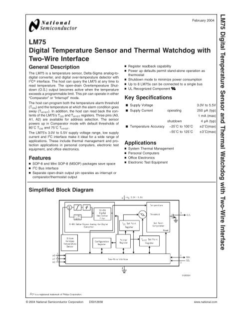
LM75 Digital Temperature Sensor and Thermal ... - HEStore.hu
LM75 Digital Temperature Sensor and Thermal ... - HEStore.hu
LM75 Digital Temperature Sensor and Thermal ... - HEStore.hu

You also want an ePaper? Increase the reach of your titles
YUMPU automatically turns print PDFs into web optimized ePapers that Google loves.
<strong>LM75</strong><br />
<strong>Digital</strong> <strong>Temperature</strong> <strong>Sensor</strong> <strong>and</strong> <strong>Thermal</strong> Watchdog with<br />
Two-Wire Interface<br />
General Description<br />
The <strong>LM75</strong> is a temperature sensor, Delta-Sigma analog-todigital<br />
converter, <strong>and</strong> digital over-temperature detector with<br />
I 2 C ® interface. The host can query the <strong>LM75</strong> at any time to<br />
read temperature. The open-drain Overtemperature S<strong>hu</strong>tdown<br />
(O.S.) output becomes active when the temperature<br />
exceeds a programmable limit. This pin can operate in either<br />
“Comparator” or “Interrupt” mode.<br />
The host can program both the temperature alarm threshold<br />
(T OS ) <strong>and</strong> the temperature at which the alarm condition goes<br />
away (T HYST ). In addition, the host can read back the contents<br />
of the <strong>LM75</strong>’s T OS <strong>and</strong> T HYST registers. Three pins (A0,<br />
A1, A2) are available for address selection. The sensor<br />
powers up in Comparator mode with default thresholds of<br />
80˚C T OS <strong>and</strong> 75˚C T HYST .<br />
The <strong>LM75</strong>’s 3.0V to 5.5V supply voltage range, low supply<br />
current <strong>and</strong> I 2 C interface make it ideal for a wide range of<br />
applications. These include thermal management <strong>and</strong> protection<br />
applications in personal computers, electronic test<br />
equipment, <strong>and</strong> office electronics.<br />
Features<br />
n SOP-8 <strong>and</strong> Mini SOP-8 (MSOP) packages save space<br />
n I 2 C Bus interface<br />
n Separate open-drain output pin operates as interrupt or<br />
comparator/thermostat output<br />
Simplified Block Diagram<br />
n Register readback capability<br />
n Power up defaults permit st<strong>and</strong>-alone operation as<br />
thermostat<br />
n S<strong>hu</strong>tdown mode to minimize power consumption<br />
n Up to 8 <strong>LM75</strong>s can be connected to a single bus<br />
n UL Recognized Component<br />
Key Specifications<br />
j Supply Voltage 3.0V to 5.5V<br />
j Supply Current operating 250 µA (typ)<br />
1 mA (max)<br />
s<strong>hu</strong>tdown<br />
4 µA (typ)<br />
j <strong>Temperature</strong> Accuracy −25˚C to 100˚C ±2˚C(max)<br />
−55˚C to 125˚C ±3˚C(max)<br />
Applications<br />
n System <strong>Thermal</strong> Management<br />
n Personal Computers<br />
n Office Electronics<br />
n Electronic Test Equipment<br />
February 2004<br />
<strong>LM75</strong> <strong>Digital</strong> <strong>Temperature</strong> <strong>Sensor</strong> <strong>and</strong> <strong>Thermal</strong> Watchdog with Two-Wire Interface<br />
01265801<br />
I 2 C ® is a registered trademark of Philips Corporation.<br />
© 2004 National Semiconductor Corporation DS012658 www.national.com
<strong>LM75</strong><br />
Connection Diagram<br />
SOP-8 <strong>and</strong> Mini SOP-8<br />
01265802<br />
Ordering Information<br />
Order Number<br />
Package<br />
Marking<br />
NS Package<br />
Number<br />
Supply<br />
Voltage<br />
Transport Media<br />
Noise Filter<br />
on SDA <strong>and</strong><br />
SCL<br />
<strong>LM75</strong>BIM-3 <strong>LM75</strong>BIM-3 M08A (SOP-8) 3.3V 95 Units in Rail Yes<br />
<strong>LM75</strong>BIMX-3 <strong>LM75</strong>BIM-3 M08A (SOP-8) 3.3V 2500 Units on Tape <strong>and</strong> Reel Yes<br />
<strong>LM75</strong>BIMM-3 T01B MUA08A (MSOP-8) 3.3V 1000 Units on Tape <strong>and</strong> Reel Yes<br />
<strong>LM75</strong>BIMMX-3 T01B MUA08A (MSOP-8) 3.3V 3500 Units on Tape <strong>and</strong> Reel Yes<br />
<strong>LM75</strong>BIM-5 <strong>LM75</strong>BIM-5 M08A (SOP-8) 5V 95 Units in Rail Yes<br />
<strong>LM75</strong>BIMX-5 <strong>LM75</strong>BIM-5 M08A (SOP-8) 5V 2500 Units on Tape <strong>and</strong> Reel Yes<br />
<strong>LM75</strong>BIMM-5 T00B MUA08A (MSOP-8) 5V 1000 Units on Tape <strong>and</strong> Reel Yes<br />
<strong>LM75</strong>BIMMX-5 T00B MUA08A (MSOP-8) 5V 3500 Units on Tape <strong>and</strong> Reel Yes<br />
<strong>LM75</strong>CIM-3 <strong>LM75</strong>CIM-3 M08A (SOP-8) 3.3V 95 Units in Rail Not Available<br />
<strong>LM75</strong>CIMX-3 <strong>LM75</strong>CIM-3 M08A (SOP-8) 3.3V 2500 Units on Tape <strong>and</strong> Reel Not Available<br />
<strong>LM75</strong>CIMM-3 T01C MUA08A (MSOP-8) 3.3V 1000 Units on Tape <strong>and</strong> Reel Not Available<br />
<strong>LM75</strong>CIMMX-3 T01C MUA08A (MSOP-8) 3.3V 3500 Units on Tape <strong>and</strong> Reel Not Available<br />
<strong>LM75</strong>CIM-5 <strong>LM75</strong>CIM-5 M08A (SOP-8) 5V 95 Units in Rail Not Available<br />
<strong>LM75</strong>CIMX-5 <strong>LM75</strong>CIM-5 M08A (SOP-8) 5V 2500 Units on Tape <strong>and</strong> Reel Not Available<br />
<strong>LM75</strong>CIMM-5 T00C MUA08A (MSOP-8) 5V 1000 Units on Tape <strong>and</strong> Reel Not Available<br />
<strong>LM75</strong>CIMMX-5 T00C MUA08A (MSOP-8) 5V 3500 Units on Tape <strong>and</strong> Reel Not Available<br />
Pin Description<br />
Label Pin # Function Typical Connection<br />
SDA 1 I 2 C Serial Bi-Directional Data Line. Open Drain. From Controller, tied to a pull-up<br />
SCL 2 I 2 C Clock Input From Controller<br />
O.S. 3 Overtemperature S<strong>hu</strong>tdown Open Drain Output Pull–up Resistor, Controller Interrupt Line<br />
GND 4 Power Supply Ground Ground<br />
+V S 8 Positive Supply Voltage Input DC Voltage from 3V to 5.5V; 0.1µF bypass<br />
capacitor with 10µF bulk capacitance in the<br />
near vicinity<br />
A0–A2 7,6,5 User-Set I 2 C Address Inputs Ground (Low, “0”) or +V S (High, “1”)<br />
www.national.com 2
Pin Description (Continued)<br />
<strong>LM75</strong><br />
01265803<br />
FIGURE 1. Typical Application<br />
3<br />
www.national.com
<strong>LM75</strong><br />
Absolute Maximum Ratings (Note 1)<br />
Supply Voltage −0.3V to 6.5V<br />
Voltage at any Pin −0.3V to +V S + 0.3V<br />
Input Current at any Pin (Note 2)<br />
5 mA<br />
Package Input Current (Note 2)<br />
20 mA<br />
O.S. Output Sink Current<br />
10 mA<br />
O.S. Output Voltage 6.5V<br />
Storage <strong>Temperature</strong><br />
−65˚C to +150˚C<br />
Soldering Information, Lead <strong>Temperature</strong><br />
SOP <strong>and</strong> MSOP Package (Note 3)<br />
Vapor Phase (60 seconds)<br />
Infrared (15 seconds)<br />
215˚C<br />
220˚C<br />
ESD Susceptibility (Note 4) <strong>LM75</strong>B <strong>LM75</strong>C<br />
Human Body Model 2500V 1500V<br />
Machine Model 250V 100V<br />
Operating Ratings<br />
Specified <strong>Temperature</strong> Range<br />
T MIN to T MAX<br />
(Note 5)<br />
−55˚C to +125˚C<br />
Supply Voltage Range (+V S )<br />
+3.0V to +5.5V<br />
<strong>Temperature</strong>-to-<strong>Digital</strong> Converter Characteristics<br />
Unless otherwise noted, these specifications apply for +V S = +5 Vdc for <strong>LM75</strong>BIM-5, <strong>LM75</strong>BIMM-5, <strong>LM75</strong>CIM-5, <strong>and</strong><br />
<strong>LM75</strong>CIMM-5 <strong>and</strong> +V S = +3.3 Vdc for <strong>LM75</strong>BIM-3, <strong>LM75</strong>BIMM-3, <strong>LM75</strong>CIM-3, <strong>and</strong> <strong>LM75</strong>CIMM-3 (Note 6). Boldface limits<br />
apply for T A =T J =T MIN to T MAX ; all other limits T A =T J = +25˚C, unless otherwise noted.<br />
Parameter<br />
Conditions<br />
Typical<br />
(Note 12)<br />
Limits<br />
(Note 7)<br />
Units<br />
(Limit)<br />
Accuracy T A = −25˚C to +100˚C ±2.0 ˚C (max)<br />
T A = −55˚C to +125˚C ±3.0 ˚C (max)<br />
Resolution 9 Bits<br />
<strong>Temperature</strong> Conversion Time (Note 8) 100 ms<br />
Quiescent Current <strong>LM75</strong>B I 2 C Inactive 0.25 0.5 mA (max)<br />
S<strong>hu</strong>tdown Mode, +V S =3V 4 µA<br />
S<strong>hu</strong>tdown Mode, +V S =5V 6 µA<br />
<strong>LM75</strong>C I 2 C Inactive 0.25 1.0 mA (max)<br />
S<strong>hu</strong>tdown Mode, +V S =3V 4 µA<br />
S<strong>hu</strong>tdown Mode, +V S =5V 6 µA<br />
O.S. Output Saturation Voltage I OUT = 4.0 mA 0.8 V (max)<br />
(Note 9)<br />
O.S. Delay (Note 10) 1 Conversions (min)<br />
6 Conversions (max)<br />
T OS Default <strong>Temperature</strong> (Note 11) 80 ˚C<br />
T HYST Default <strong>Temperature</strong> (Note 11) 75 ˚C<br />
Logic Electrical Characteristics<br />
DIGITAL DC CHARACTERISTICS Unless otherwise noted, these specifications apply for +V S = +5 Vdc for <strong>LM75</strong>BIM-5,<br />
<strong>LM75</strong>BIMM-5, <strong>LM75</strong>CIM-5, <strong>and</strong> <strong>LM75</strong>CIMM-5 <strong>and</strong> +V S = +3.3 Vdc for <strong>LM75</strong>BIM-3, <strong>LM75</strong>BIMM-3, <strong>LM75</strong>CIM-3, <strong>and</strong><br />
<strong>LM75</strong>CIMM-3 (Note 6). Boldface limits apply for T A =T J =T MIN to T MAX ; all other limits T A =T J = +25˚C, unless otherwise<br />
noted.<br />
Symbol Parameter Conditions<br />
Typical<br />
(Note 12)<br />
Limits<br />
(Note 7)<br />
Units<br />
(Limit)<br />
V IN(1) Logical “1” Input Voltage +V S x 0.7 V (min)<br />
+V S + 0.5 V (max)<br />
V IN(0) Logical “0” Input Voltage −0.3 V (min)<br />
+V S x 0.3 V (max)<br />
I IN(1) Logical “1” Input Current V IN = 5V 0.005 1.0 µA (max)<br />
I IN(0) Logical “0” Input Current V IN = 0V −0.005 −1.0 µA (max)<br />
C IN All <strong>Digital</strong> Inputs 20 pF<br />
I OH High Level Output Current V OH =5V 100 µA (max)<br />
V OL Low Level Output Voltage I OL =3mA 0.4 V (max)<br />
t OF Output Fall Time C L = 400 pF 250 ns (max)<br />
www.national.com 4
Logic Electrical Characteristics (Continued)<br />
DIGITAL DC CHARACTERISTICS Unless otherwise noted, these specifications apply for +V S = +5 Vdc for <strong>LM75</strong>BIM-5,<br />
<strong>LM75</strong>BIMM-5, <strong>LM75</strong>CIM-5, <strong>and</strong> <strong>LM75</strong>CIMM-5 <strong>and</strong> +V S = +3.3 Vdc for <strong>LM75</strong>BIM-3, <strong>LM75</strong>BIMM-3, <strong>LM75</strong>CIM-3, <strong>and</strong><br />
<strong>LM75</strong>CIMM-3 (Note 6). Boldface limits apply for T A =T J =T MIN to T MAX ; all other limits T A =T J = +25˚C, unless otherwise<br />
noted.<br />
<strong>LM75</strong><br />
Symbol Parameter Conditions<br />
Typical<br />
(Note 12)<br />
Limits<br />
(Note 7)<br />
Units<br />
(Limit)<br />
I O =3mA<br />
I 2 C DIGITAL SWITCHING CHARACTERISTICS Unless otherwise noted, these specifications apply for +V S = +5 Vdc for<br />
<strong>LM75</strong>BIM-5, <strong>LM75</strong>BIMM-5, <strong>LM75</strong>CIM-5, <strong>and</strong> <strong>LM75</strong>CIMM-5 <strong>and</strong> +V S = +3.3 Vdc for <strong>LM75</strong>BIM-3, <strong>LM75</strong>BIMM-3, <strong>LM75</strong>CIM-3,<br />
<strong>and</strong> <strong>LM75</strong>CIMM-3. C L (load capacitance) on output lines = 80 pF unless otherwise specified. Boldface limits apply for T A =<br />
T J =T MIN to T MAX ; all other limits T A =T J = +25˚C, unless otherwise noted. The switching characteristics of the <strong>LM75</strong> fully<br />
meet or exceed the published specifications of the I 2 C bus. The following parameters are the timing relationships between SCL<br />
<strong>and</strong> SDA signals related to the <strong>LM75</strong>. They are not the I 2 C bus specifications.<br />
Symbol Parameter Conditions<br />
Typical<br />
(Note 12)<br />
Limits<br />
(Note 7)<br />
Units<br />
(Limit)<br />
t 1 SCL (Clock) Period 2.5 µs (min)<br />
t 2 Data in Set-Up Time to SCL High 100 ns (min)<br />
t 3 Data Out Stable after SCL Low 0 ns (min)<br />
t 4 SDA Low Set-Up Time to SCL Low (Start Condition) 100 ns (min)<br />
t 5 SDA High Hold Time after SCL High (Stop Condition) 100 ns (min)<br />
t TIMEOUT SDA Time Low for Reset of Serial Interface (Note 13) <strong>LM75</strong>B 75<br />
325<br />
<strong>LM75</strong>C<br />
Not<br />
Applicable<br />
ms (min)<br />
ms (max)<br />
01265804<br />
Note 1: Absolute Maximum Ratings indicate limits beyond which damage to the device may occur. DC <strong>and</strong> AC electrical specifications do not apply when operating<br />
the device beyond its rated operating conditions.<br />
Note 2: When the input voltage (V I ) at any pin exceeds the power supplies (V I < GND or V I > +V S ) the current at that pin should be limited to 5 mA. The 20 mA<br />
maximum package input current rating limits the number of pins that can safely exceedthe power supplies with an input current of 5 mA to four.<br />
Note 3: See AN-450 “Surface Mounting Methods <strong>and</strong> Their Effect on Product Reliability” or the section titled “Surface Mount” found in a current National<br />
Semiconductor Linear Data Book for other methods of soldering surface mount devices.<br />
Note 4: Human body model, 100 pF discharged through a 1.5 kΩ resistor. Machine model, 200 pF discharged directly into each pin.<br />
5<br />
www.national.com
<strong>LM75</strong><br />
Note 5: <strong>LM75</strong> θ JA (thermal resistance, junction-to-ambient) when attached to a printed circuit board with 2 oz. foil similar to the one shown in Figure 3 is summarized<br />
in the table below:<br />
Device Number<br />
NS Package<br />
Number<br />
<strong>Thermal</strong><br />
Resistance (θ JA )<br />
<strong>LM75</strong>BIM-3, <strong>LM75</strong>BIM-5, <strong>LM75</strong>CIM-3, <strong>LM75</strong>CIM-5 M08A 200˚C/W<br />
<strong>LM75</strong>BIMM-3, <strong>LM75</strong>BIMM-5, <strong>LM75</strong>CIMM-3, <strong>LM75</strong>CIMM-5 MUA08A 250˚C/W<br />
Note 6: All part numbers of the <strong>LM75</strong> will operate properly over the +V S supply voltage range of 3V to 5.5V. The devices are tested <strong>and</strong> specified for rated accuracy<br />
at their nominal supply voltage. Accuracy will typically degrade 1˚C/V of variation in +V S as it varies from the nominal value.<br />
Note 7: Limits are guaranteed to National’s AOQL (Average Outgoing Quality Level).<br />
Note 8: This specification is provided only to indicate how often temperature data is updated. The <strong>LM75</strong> can be read at any time without regard to conversion state<br />
(<strong>and</strong> will yield last conversion result). If a conversion is in process it will be interrupted <strong>and</strong> restarted after the end of the read.<br />
Note 9: For best accuracy, minimize output loading. Higher sink currents can affect sensor accuracy with internal heating. This can cause an error of 0.64˚C at full<br />
rated sink current <strong>and</strong> saturation voltage based on junction-to-ambient thermal resistance.<br />
Note 10: O.S. Delay is user programmable up to 6 “over limit” conversions before O.S. is set to minimize false tripping in noisy environments.<br />
Note 11: Default values set at power up.<br />
Note 12: Typicals are at T A = 25˚C <strong>and</strong> represent most likely parametric norm.<br />
Note 13: Holding the SDA line low for a time greater than t TIMEOUT will cause the <strong>LM75</strong>B to reset SDA to the IDLE state of the serial bus communication (SDA set<br />
High).<br />
01265805<br />
FIGURE 2. <strong>Temperature</strong>-to-<strong>Digital</strong> Transfer Function (Non-linear scale for clarity)<br />
www.national.com 6
<strong>LM75</strong><br />
01265806<br />
FIGURE 3. Printed Circuit Board Used for <strong>Thermal</strong> Resistance Specifications<br />
Typical Performance Characteristics<br />
Static Quiescent Current vs<br />
<strong>Temperature</strong><br />
Dynamic Quiescent Current vs<br />
<strong>Temperature</strong><br />
Accuracy vs <strong>Temperature</strong><br />
01265816 01265817 01265818<br />
1.0 Functional Description<br />
The <strong>LM75</strong> temperature sensor incorporates a b<strong>and</strong>-gap type<br />
temperature sensor <strong>and</strong> 9-bit ADC (Delta-Sigma Analog-to-<br />
<strong>Digital</strong> Converter). The temperature data output of the <strong>LM75</strong><br />
is available at all times via the I 2 C bus. If a conversion is in<br />
progress, it will be stopped <strong>and</strong> restarted after the read. A<br />
digital comparator is also incorporated that compares a series<br />
of readings, the number of which is user-selectable, to<br />
user-programmable setpoint <strong>and</strong> hysteresis values. The<br />
comparator trips the O.S. output line, which is programmable<br />
for mode <strong>and</strong> polarity.<br />
The <strong>LM75</strong>B contains all the functionality of the <strong>LM75</strong>C, plus<br />
two additional features:<br />
1. The <strong>LM75</strong>B has an integrated low-pass filter on both the<br />
SDA <strong>and</strong> the SCL line. These filters increase communications<br />
reliability in noisy environments.<br />
2. The <strong>LM75</strong>B also has a bus fault timeout feature. If the<br />
SDA line is held low for longer than t TIMEOUT (75 ms<br />
minimum to 325 ms maximum) the <strong>LM75</strong>B will reset to<br />
the IDLE state (SDA set to high impedance) <strong>and</strong> wait for<br />
a new start condition.<br />
1.1 O.S. OUTPUT, T OS AND T HYST LIMITS<br />
In Comparator mode the O.S. Output behaves like a thermostat.<br />
The output becomes active when temperature exceeds<br />
the T OS limit, <strong>and</strong> leaves the active state when the<br />
temperature drops below the T HYST limit. In this mode the<br />
O.S. output can be used to turn a cooling fan on, initiate an<br />
emergency system s<strong>hu</strong>tdown, or reduce system clock<br />
speed. S<strong>hu</strong>tdown mode does not reset O.S. state in a comparator<br />
mode.<br />
In Interrupt mode exceeding T OS also makes O.S. active but<br />
O.S. will remain active indefinitely until reset by reading any<br />
register via the I 2 C interface. Once O.S. has been activated<br />
7<br />
www.national.com
<strong>LM75</strong><br />
1.0 Functional Description (Continued)<br />
by crossing T OS , then reset, it can be activated again only by<br />
<strong>Temperature</strong> going below T HYST . Again, it will remain active<br />
indefinitely until being reset by a read. Placing the <strong>LM75</strong> in<br />
s<strong>hu</strong>tdown mode also resets the O.S. Output.<br />
1.2 POWER UP AND POWER DOWN<br />
The <strong>LM75</strong> always powers up in a known state. The power up<br />
default conditions are:<br />
1. Comparator mode<br />
2. T OS = 80˚C<br />
3. T HYST = 75˚C<br />
4. O.S. active low<br />
5. Pointer = “00”<br />
If the <strong>LM75</strong> is not connected to the I 2 C bus on power up, it<br />
will act as a st<strong>and</strong>-alone thermostat with the above temperature<br />
settings.<br />
When the supply voltage is less than about 1.7V, the <strong>LM75</strong> is<br />
considered powered down. As the supply voltage rises<br />
above the nominal 1.7V power up threshold, the internal<br />
registers are reset to the power up default values listed<br />
above.<br />
1.3 I 2 C BUS INTERFACE<br />
The <strong>LM75</strong> operates as a slave on the I 2 C bus, so the SCL<br />
line is an input (no clock is generated by the <strong>LM75</strong>) <strong>and</strong> the<br />
SDA line is a bi-directional serial data path. According to I 2 C<br />
bus specifications, the <strong>LM75</strong> has a 7-bit slave address. The<br />
four most significant bits of the slave address are hard wired<br />
inside the <strong>LM75</strong> <strong>and</strong> are “1001”. The three least significant<br />
bits of the address are assigned to pins A2–A0, <strong>and</strong> are set<br />
by connecting these pins to ground for a low, (0); or to +V S<br />
for a high, (1).<br />
Therefore, the complete slave address is:<br />
1 0 0 1 A2 A1 A0<br />
MSB<br />
LSB<br />
01265807<br />
Note 14: These interrupt mode resets of O.S. occur only when <strong>LM75</strong> is read or placed in s<strong>hu</strong>tdown. Otherwise, O.S. would remain active indefinitely for any event.<br />
FIGURE 4. O.S. Output <strong>Temperature</strong> Response Diagram<br />
www.national.com 8
1.0 Functional Description (Continued)<br />
1.4 TEMPERATURE DATA FORMAT<br />
<strong>Temperature</strong> data can be read from the <strong>Temperature</strong>, T OS<br />
Set Point, <strong>and</strong> T HYST Set Point registers; <strong>and</strong> written to the<br />
T OS Set Point, <strong>and</strong> T HYST Set Point registers. <strong>Temperature</strong><br />
data is represented by a 9-bit, two’s complement word with<br />
an LSB (Least Significant Bit) equal to 0.5˚C:<br />
<strong>Temperature</strong><br />
<strong>Digital</strong> Output<br />
Binary<br />
Hex<br />
+125˚C 0 1111 1010 0FAh<br />
+25˚C 0 0011 0010 032h<br />
+0.5˚C 0 0000 0001 001h<br />
0˚C 0 0000 0000 000h<br />
−0.5˚C 1 1111 1111 1FFh<br />
−25˚C 1 1100 1110 1CEh<br />
−55˚C 1 1001 0010 192h<br />
1.5 SHUTDOWN MODE<br />
S<strong>hu</strong>tdown mode is enabled by setting the s<strong>hu</strong>tdown bit in the<br />
Configuration register via the I 2 C bus. S<strong>hu</strong>tdown mode reduces<br />
power supply current to 4 µA typical. In Interrupt mode<br />
O.S. is reset if previously set <strong>and</strong> is undefined in Comparator<br />
mode during s<strong>hu</strong>tdown. The I 2 C interface remains active.<br />
Activity on the clock <strong>and</strong> data lines of the I 2 C bus may<br />
slightly increase s<strong>hu</strong>tdown mode quiescent current. T OS ,<br />
T HYST , <strong>and</strong> Configuration registers can be read from <strong>and</strong><br />
written to in s<strong>hu</strong>tdown mode.<br />
1.6 FAULT QUEUE<br />
A fault queue of up to 6 faults is provided to prevent false<br />
tripping of O.S. when the <strong>LM75</strong> is used in noisy environments.<br />
The number of faults set in the queue must occur<br />
consecutively to set the O.S. output.<br />
1.7 COMPARATOR/INTERRUPT MODE<br />
As indicated in the O.S. Output <strong>Temperature</strong> Response Diagram,<br />
Figure 4, the events that trigger O.S. are identical for<br />
either Comparator or Interrupt mode. The most important<br />
difference is that in Interrupt mode the O.S. will remain set<br />
indefinitely once it has been set. To reset O.S. while in<br />
Interrupt mode, perform a read from any register in the<br />
<strong>LM75</strong>.<br />
1.8 O.S. OUTPUT<br />
The O.S. output is an open-drain output <strong>and</strong> does not have<br />
an internal pull-up. A “high” level will not be observed on this<br />
pin until pull-up current is provided from some external<br />
source, typically a pull-up resistor. Choice of resistor value<br />
depends on many system factors but, in general, the pull-up<br />
resistor should be as large as possible. This will minimize<br />
any errors due to internal heating of the <strong>LM75</strong>. The maximum<br />
resistance of the pull up, based on <strong>LM75</strong> specification<br />
for High Level Output Current, to provide a 2V high level, is<br />
30 kΩ.<br />
1.9 O.S. POLARITY<br />
The O.S. output can be programmed via the configuration<br />
register to be either active low (default mode), or active high.<br />
In active low mode the O.S. output goes low when triggered<br />
exactly as shown on the O.S. Output <strong>Temperature</strong> Response<br />
Diagram, Figure 4. Active high simply inverts the polarity of<br />
the O.S. output.<br />
<strong>LM75</strong><br />
9<br />
www.national.com
<strong>LM75</strong><br />
1.0 Functional Description (Continued)<br />
1.10 INTERNAL REGISTER STRUCTURE<br />
01265808<br />
There are four data registers in the <strong>LM75</strong>, selected by the<br />
Pointer register. At power-up the Pointer is set to “00”; the<br />
location for the <strong>Temperature</strong> Register. The Pointer register<br />
latches whatever the last location it was set to. In Interrupt<br />
Mode, a read from the <strong>LM75</strong>, or placing the device in s<strong>hu</strong>tdown<br />
mode, resets the O.S. output. All registers are read<br />
<strong>and</strong> write, except the <strong>Temperature</strong> register which is read<br />
only.<br />
A write to the <strong>LM75</strong> will always include the address byte <strong>and</strong><br />
the Pointer byte. A write to the Configuration register requires<br />
one data byte, <strong>and</strong> the T OS <strong>and</strong> T HYST registers<br />
require two data bytes.<br />
Reading the <strong>LM75</strong> can take place either of two ways: If the<br />
location latched in the Pointer is correct (most of the time it is<br />
expected that the Pointer will point to the <strong>Temperature</strong> register<br />
because it will be the data most frequently read from the<br />
<strong>LM75</strong>), then the read can simply consist of an address byte,<br />
followed by retrieving the corresponding number of data<br />
bytes. If the Pointer needs to be set, then an address byte,<br />
pointer byte, repeat start, <strong>and</strong> another address byte will<br />
accomplish a read.<br />
The first data byte is the most significant byte with most<br />
significant bit first, permitting only as much data as necessary<br />
to be read to determine temperature condition. For<br />
instance, if the first four bits of the temperature data indicates<br />
an overtemperature condition, the host processor<br />
could immediately take action to remedy the excessive temperatures.<br />
At the end of a read, the <strong>LM75</strong> can accept either<br />
Acknowledge or No Acknowledge from the Master (No Acknowledge<br />
is typically used as a signal for the slave that the<br />
Master has read its last byte).<br />
An inadvertent 8-bit read from a 16-bit register, with the D7<br />
bit low, can cause the <strong>LM75</strong> to stop in a state where the SDA<br />
line is held low as shown in Figure 5. This can prevent any<br />
further bus communication until at least 9 additional clock<br />
cycles have occurred. Alternatively, the master can issue<br />
clock cycles until SDA goes high, at which time issuing a<br />
“Stop” condition will reset the <strong>LM75</strong>.<br />
01265809<br />
FIGURE 5. Inadvertent 8-Bit Read from 16-Bit Register where D7 is Zero (“0”)<br />
www.national.com 10
1.0 Functional Description (Continued)<br />
1.11 POINTER REGISTER<br />
(Selects which registers will be read from or written to):<br />
<strong>LM75</strong><br />
P7 P6 P5 P4 P3 P2 P1 P0<br />
0 0 0 0 0 0 Register<br />
Select<br />
P0-P1: Register Select:<br />
P1 P0 Register<br />
0 0 <strong>Temperature</strong> (Read only) (Power-up default)<br />
0 1 Configuration (Read/Write)<br />
1 0 T HYST (Read/Write)<br />
1 1 T OS (Read/Write)<br />
P2–P7: Must be kept zero.<br />
1.12 TEMPERATURE REGISTER<br />
(Read Only):<br />
D15 D14 D13 D12 D11 D10 D9 D8 D7 D6 D5 D4 D3 D2 D1 D0<br />
MSB Bit 7 Bit 6 Bit 5 Bit 4 Bit 3 Bit 2 Bit 1 LSB X X X X X X X<br />
D0–D6: Undefined<br />
D7–D15: <strong>Temperature</strong> Data. One LSB = 0.5˚C. Two’s<br />
complement format.<br />
1.13 CONFIGURATION REGISTER<br />
(Read/Write):<br />
D7 D6 D5 D4 D3 D2 D1 D0<br />
0 0 0 Fault Queue O.S. Cmp/Int S<strong>hu</strong>tdown<br />
Polarity<br />
Power up default is with all bits “0” (zero).<br />
D0: S<strong>hu</strong>tdown: When set to 1 the <strong>LM75</strong> goes to low power<br />
s<strong>hu</strong>tdown mode.<br />
D1: Comparator/Interrupt mode: 0 is Comparator mode, 1 is<br />
Interrupt mode.<br />
D2: O.S. Polarity: 0 is active low, 1 is active high. O.S. is an<br />
open-drain output under all conditions.<br />
D3–D4: Fault Queue: Number of faults necessary to detect<br />
before setting O.S. output to avoid false tripping due to<br />
noise. Faults are determind at the end of a conversion.<br />
Conversions take about 100 ms, typically, to complete.<br />
D4 D3 Number of Faults<br />
0 0 1 (Power-up default)<br />
0 1 2<br />
1 0 4<br />
1 1 6<br />
D5–D7: These bits are used for production testing <strong>and</strong> must<br />
be kept zero for normal operation.<br />
1.14 T HYST AND T OS REGISTER<br />
(Read/Write):<br />
D15 D14 D13 D12 D11 D10 D9 D8 D7 D6 D5 D4 D3 D2 D1 D0<br />
MSB Bit 7 Bit 6 Bit 5 Bit 4 Bit 3 Bit 2 Bit 1 LSB X X X X X X X<br />
D0–D6: Undefined<br />
D7–D15: T HYST Or T OS Trip <strong>Temperature</strong> Data. Power up<br />
default is T OS = 80˚C, T HYST = 75˚C.<br />
11<br />
www.national.com
2.0 I 2 C Timing Diagrams<br />
01265810<br />
FIGURE 6. Timing Diagram<br />
<strong>LM75</strong><br />
www.national.com 12
<strong>LM75</strong><br />
2.0 I 2 C Timing Diagrams (Continued)<br />
01265811<br />
FIGURE 7. Timing Diagrams (Continued)<br />
13<br />
www.national.com
<strong>LM75</strong><br />
3.0 Application Hints<br />
To get the expected results when measuring temperature<br />
with an integrated circuit temperature sensor like the <strong>LM75</strong>,<br />
it is important to underst<strong>and</strong> that the sensor measures its<br />
own die temperature. For the <strong>LM75</strong>, the best thermal path<br />
between the die <strong>and</strong> the outside world is through the <strong>LM75</strong>’s<br />
pins. In the MSOP-8 package, the GND pin is directly connected<br />
to the die, so the GND pin provides the best thermal<br />
path. If the other pins are at different temperatures (unlikely,<br />
but possible), they will affect the die temperature, but not as<br />
strongly as the GND pin. In the SO-8 package, none of the<br />
pins is directly connected to the die, so they will all contribute<br />
similarly to the die temperature. Because the pins represent<br />
a good thermal path to the <strong>LM75</strong> die, the <strong>LM75</strong> will provide<br />
an accurate measurement of the temperature of the printed<br />
circuit board on which it is mounted. There is a less efficient<br />
thermal path between the plastic package <strong>and</strong> the <strong>LM75</strong> die.<br />
If the ambient air temperature is significantly different from<br />
the printed circuit board temperature, it will have a small<br />
effect on the measured temperature.<br />
In probe-type applications, the <strong>LM75</strong> can be mounted inside<br />
a sealed-end metal tube, <strong>and</strong> can then be dipped into a bath<br />
or screwed into a threaded hole in a tank. As with any IC, the<br />
<strong>LM75</strong> <strong>and</strong> accompanying wiring <strong>and</strong> circuits must be kept<br />
insulated <strong>and</strong> dry, to avoid leakage <strong>and</strong> corrosion. This is<br />
especially true if the circuit may operate at cold temperatures<br />
where condensation can occur. Printed-circuit coatings <strong>and</strong><br />
varnishes such as Humiseal <strong>and</strong> epoxy paints or dips are<br />
often used to insure that moisture cannot corrode the <strong>LM75</strong><br />
or its connections.<br />
4.0 Typical Applications<br />
DIGITAL NOISE ISSUES<br />
The <strong>LM75</strong>B features an integrated low-pass filter on both the<br />
SCL <strong>and</strong> the SDA digital lines to mitigate the effects of bus<br />
noise. Although this filtering makes the <strong>LM75</strong>B communication<br />
robust in noisy environments, good layout practices are<br />
always recommended. Minimize noise coupling by keeping<br />
digital traces away from switching power supplies. Also,<br />
ensure that digital lines containing high-speed data communications<br />
cross at right angles to the SDA <strong>and</strong> SCL lines.<br />
Excessive noise coupling into the SDA <strong>and</strong> SCL lines on the<br />
<strong>LM75</strong>C — specifically noise with amplitude greater than 400<br />
mV pp (the <strong>LM75</strong>’s typical hysteresis), overshoot greater than<br />
300 mV above +V s , <strong>and</strong> undershoot more than 300 mV<br />
below GND — may prevent successful serial communication<br />
with the <strong>LM75</strong>C. Serial bus no-acknowledge is the most<br />
common symptom, causing unnecessary traffic on the bus.<br />
The layout procedures mentioned above apply also to the<br />
<strong>LM75</strong>C. Although the serial bus maximum frequency of communication<br />
is only 100 kHz, care must be taken to ensure<br />
proper termination within a system with long printed circuit<br />
board traces or multiple parts on the bus. Resistance can be<br />
added in series with the SDA <strong>and</strong> SCL lines to further help<br />
filter noise <strong>and</strong> ringing. A 5 kΩ resistor should be placed in<br />
series with the SCL line, placed as close as possible to the<br />
SCL pin on the <strong>LM75</strong>C. This 5 kΩ resistor, with the 5 pF to 10<br />
pF stray capacitance of the <strong>LM75</strong> provides a 6 MHz to 12<br />
MHz low pass filter, which is sufficient filtering in most cases.<br />
01265812<br />
When using the two-wire interface: program O.S. for active high <strong>and</strong> connect O.S. directly to Q2’s gate.<br />
FIGURE 8. Simple Fan Controller, Interface Optional<br />
www.national.com 14
4.0 Typical Applications (Continued)<br />
<strong>LM75</strong><br />
01265813<br />
FIGURE 9. Data Acquisition System with <strong>Temperature</strong> Input via I 2 C Bus<br />
01265814<br />
FIGURE 10. Simple Thermostat, Interface Optional<br />
15<br />
www.national.com
<strong>LM75</strong><br />
4.0 Typical Applications (Continued)<br />
01265815<br />
FIGURE 11. <strong>Temperature</strong> <strong>Sensor</strong> with Loudmouth Alarm (Barking Watchdog)<br />
www.national.com 16
Physical Dimensions inches (millimeters) unless otherwise noted<br />
<strong>LM75</strong><br />
8-Lead (0.150" Wide) Molded Small Outline Package (SOP), JEDEC<br />
Order Number <strong>LM75</strong>CIM-3, <strong>LM75</strong>CIMX-3, <strong>LM75</strong>CIM-5, <strong>LM75</strong>CIMX-5,<br />
<strong>LM75</strong>BIM-3, <strong>LM75</strong>BIMX-3, <strong>LM75</strong>BIM-5, or <strong>LM75</strong>BIMX-5<br />
NS Package Number M08A<br />
17<br />
www.national.com
<strong>LM75</strong> <strong>Digital</strong> <strong>Temperature</strong> <strong>Sensor</strong> <strong>and</strong> <strong>Thermal</strong> Watchdog with Two-Wire Interface<br />
Physical Dimensions inches (millimeters) unless otherwise noted (Continued)<br />
LIFE SUPPORT POLICY<br />
8-Lead Molded Mini Small Outline Package (MSOP)<br />
(JEDEC REGISTRATION NUMBER M0-187)<br />
Order Number <strong>LM75</strong>CIMM-3, <strong>LM75</strong>CIMMX-3,<br />
<strong>LM75</strong>CIMM-5, <strong>LM75</strong>CIMMX-5,<br />
<strong>LM75</strong>BIMM-3, <strong>LM75</strong>BIMMX-3,<br />
<strong>LM75</strong>BIMM-5, or <strong>LM75</strong>BIMMX-5<br />
NS Package Number MUA08A<br />
NATIONAL’S PRODUCTS ARE NOT AUTHORIZED FOR USE AS CRITICAL COMPONENTS IN LIFE SUPPORT<br />
DEVICES OR SYSTEMS WITHOUT THE EXPRESS WRITTEN APPROVAL OF THE PRESIDENT AND GENERAL<br />
COUNSEL OF NATIONAL SEMICONDUCTOR CORPORATION. As used herein:<br />
1. Life support devices or systems are devices or<br />
systems which, (a) are intended for surgical implant<br />
into the body, or (b) support or sustain life, <strong>and</strong><br />
whose failure to perform when properly used in<br />
accordance with instructions for use provided in the<br />
labeling, can be reasonably expected to result in a<br />
significant injury to the user.<br />
BANNED SUBSTANCE COMPLIANCE<br />
2. A critical component is any component of a life<br />
support device or system whose failure to perform<br />
can be reasonably expected to cause the failure of<br />
the life support device or system, or to affect its<br />
safety or effectiveness.<br />
National Semiconductor certifies that the products <strong>and</strong> packing materials meet the provisions of the Customer Products<br />
Stewardship Specification (CSP-9-111C2) <strong>and</strong> the Banned Substances <strong>and</strong> Materials of Interest Specification<br />
(CSP-9-111S2) <strong>and</strong> contain no ‘‘Banned Substances’’ as defined in CSP-9-111S2.<br />
National Semiconductor<br />
Americas Customer<br />
Support Center<br />
Email: new.feedback@nsc.com<br />
Tel: 1-800-272-9959<br />
www.national.com<br />
National Semiconductor<br />
Europe Customer Support Center<br />
Fax: +49 (0) 180-530 85 86<br />
Email: europe.support@nsc.com<br />
Deutsch Tel: +49 (0) 69 9508 6208<br />
English Tel: +44 (0) 870 24 0 2171<br />
Français Tel: +33 (0) 1 41 91 8790<br />
National Semiconductor<br />
Asia Pacific Customer<br />
Support Center<br />
Email: ap.support@nsc.com<br />
National Semiconductor<br />
Japan Customer Support Center<br />
Fax: 81-3-5639-7507<br />
Email: jpn.feedback@nsc.com<br />
Tel: 81-3-5639-7560<br />
National does not assume any responsibility for use of any circuitry described, no circuit patent licenses are implied <strong>and</strong> National reserves the right at any time without notice to change said circuitry <strong>and</strong> specifications.


