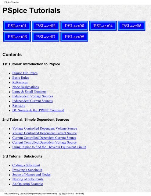
PSpice Tutorials
PSpice Tutorials
PSpice Tutorials

You also want an ePaper? Increase the reach of your titles
YUMPU automatically turns print PDFs into web optimized ePapers that Google loves.
<strong>PSpice</strong> <strong>Tutorials</strong><br />
<strong>PSpice</strong> <strong>Tutorials</strong><br />
Contents<br />
1st Tutorial: Introduction to <strong>PSpice</strong><br />
●<br />
●<br />
●<br />
●<br />
●<br />
●<br />
●<br />
●<br />
●<br />
<strong>PSpice</strong> File Types<br />
Basic Rules<br />
References<br />
Node Designations<br />
Large & Small Numbers<br />
Independent Voltage Sources<br />
Independent Current Sources<br />
Resistors<br />
DC Sweeps & the .PRINT Command<br />
2nd Tutorial: Simple Dependent Sources<br />
●<br />
●<br />
●<br />
●<br />
●<br />
Voltage Controlled Dependent Voltage Source<br />
Voltage Controlled Dependent Current Source<br />
Current Controlled Dependent Current Source<br />
Current Controlled Dependent Voltage Source<br />
Using <strong>PSpice</strong> to find the Thévenin Equivalent Circuit<br />
3rd Tutorial: Subcircuits<br />
●<br />
●<br />
●<br />
●<br />
●<br />
Coding a Subcircuit<br />
Invoking a Subcircuit<br />
Scope of Names and Nodes<br />
Nesting of Subcircuits<br />
An Op-Amp Example<br />
http://www-eng.uta.edu/evergreen/pspice/index.html (1 èç 3) [25.04.02 14:45:04]
<strong>PSpice</strong> <strong>Tutorials</strong><br />
4th Tutorial: Transient Analysis<br />
●<br />
●<br />
●<br />
●<br />
●<br />
Linear Inductors<br />
Linear Capacitors<br />
Transient Analysis<br />
Use of the .PROBE Command<br />
Example of Transient Analysis<br />
5th Tutorial: Steady State AC Analysis<br />
●<br />
●<br />
●<br />
●<br />
AC Voltage & Current Sources<br />
Use of the .PRINT AC Command<br />
Examples of AC Circuit Analysis<br />
Summary of Phasor Analysis<br />
6th Tutorial: Mutual Inductances<br />
●<br />
●<br />
●<br />
●<br />
●<br />
Basic Linear Coupled Inductors<br />
Multiple Couplings with Different Values<br />
Multiple Couplings with Same Values<br />
Nonlinear Core Model<br />
Uncoupled Nonlinear Inductors<br />
7th Tutorial: Frequency Response<br />
●<br />
●<br />
●<br />
●<br />
Frequency Range Types<br />
Using Probe for Frequency Response<br />
Examples<br />
Modifying Probe Display<br />
8th Tutorial: Special Sources<br />
●<br />
●<br />
●<br />
●<br />
●<br />
PULSE Sources<br />
SIN Sources<br />
PWL Sources<br />
LAPLACE Sources<br />
TABLE Sources<br />
http://www-eng.uta.edu/evergreen/pspice/index.html (2 èç 3) [25.04.02 14:45:04]
<strong>PSpice</strong> <strong>Tutorials</strong><br />
This site is maintained by William E. Dillon, Ph.D., P.E. To send comments, queries or suggestions click<br />
here.<br />
Last Modified: undefined<br />
http://www-eng.uta.edu/evergreen/pspice/index.html (3 èç 3) [25.04.02 14:45:04]
1st Tutorial on <strong>PSpice</strong><br />
1st Tutorial on <strong>PSpice</strong><br />
Introduction<br />
The following information concerns the text-edited version of MicroSim <strong>PSpice</strong>, version 8. It is offered<br />
here solely for the purpose of helping undergraduate students complete their classroom assignments in<br />
computer-aided circuit analysis at the University of Texas at Arlington. No other use of these notes is<br />
supported by the University of Texas at Arlington.<br />
File Types Used and Created by <strong>PSpice</strong><br />
The basic input file for <strong>PSpice</strong> is a text (ASCII) file that has the file type "CIR." In the beginning, this<br />
will be created by hand as the primary method of getting the circuit we want modeled into the <strong>PSpice</strong><br />
program. Later, when we use the schematic capture program, it will create the *.CIR file for us, along<br />
with several auxiliary file types. Do not use a word processor to create these *.CIR files unless you<br />
"Save as" text or as ASCII. You can use Notepad to edit these files, but the best editor for this purpose is<br />
the one that is provided by MicroSim, called "TextEdit."<br />
The output file always generated by <strong>PSpice</strong> is a text (ASCII) file that has the file type "OUT." I.e., if you<br />
submit a data file to <strong>PSpice</strong> named "MYCIRKUT.CIR," it will create an output file named<br />
"MYCIRKUT.OUT." This output file is created even if your run is unsuccessful due to input errors.<br />
The cause for failure is reported in the *.OUT file, so this is a good place to start looking when you need<br />
to debug your simulation model. You examine the *.OUT file with the TextEdit or Notepad programs.<br />
When everything works properly, you will find the output results in this file if you are running a DC<br />
analysis. If you are running a transient analysis or a frequency sweep analysis, there will be too much<br />
data for the *.OUT file. In these cases, we add a command to the *.CIR file that tells <strong>PSpice</strong> to save the<br />
numerical data in a *.DAT file.<br />
The aforementioned *.DAT file is by default a binary (i.e., non-ASCII) file that requires a MicroSim<br />
application called PROBE for you to see the data. PROBE is installed with <strong>PSpice</strong> from the CD-ROM.<br />
If you want, you can change the default storage format to ASCII. This is not recommended because it<br />
requires more disk space to store the data in ASCII code. Later, we will describe the procedure for<br />
invoking PROBE and creating the *.DAT file. A companion file to the *.DAT file is the *.PRB file<br />
which holds initializing information for the PROBE program.<br />
Another common method used by experienced <strong>PSpice</strong> users is the use of *.INC (include) files. These<br />
enable us to store frequently used subcircuits that have not yet been added to a library. Then we access<br />
these *.INC files with a single command line in the *.CIR file. Very convenient.<br />
Other files used with <strong>PSpice</strong> are *.LIB files where the details of complex parts are saved; we may discuss<br />
this later, but it is unlikely that we will engage in LIB file alterations until you are taking advanced<br />
http://www-eng.uta.edu/evergreen/pspice/pspice01.htm (1 èç 10) [25.04.02 14:45:30]
1st Tutorial on <strong>PSpice</strong><br />
courses.<br />
When we begin using the schematic capture program that is bundled with <strong>PSpice</strong>, we will encounter<br />
some additional file types. These are the *.SCH (the schematic data, itself), *.ALS (alias files) and<br />
*.NET (network connection files).<br />
Some Facts and Rules about <strong>PSpice</strong><br />
●<br />
●<br />
●<br />
●<br />
●<br />
●<br />
●<br />
●<br />
●<br />
<strong>PSpice</strong> is not case sensitive. This means that names such as Vbus, VBUS, vbus and even vBuS are<br />
equivalent in the program.<br />
All element names must be unique. Therefore, you can't have two resistors that are both named<br />
"Rbias," for example.<br />
The first line in the data file is used as a title. It is printed at the top of each page of output. You<br />
should use this line to store your name, the assignment, the class and any other information<br />
appropriate for a title page. <strong>PSpice</strong> will ignore this line as circuit data. Do not place any actual<br />
circuit information in the first line.<br />
There must be a node designated "0." (Zero) This is the reference node against which all voltages<br />
are calculated.<br />
Each node must have at least two elements attached to it.<br />
The last line in any data file must be ".END" (a period followed by the word "end.")<br />
All lines that are not blank (except for the title line) must have a character in column 1, the<br />
leftmost position on the line.<br />
❍ Use "*" (an asterisk) in column 1 in order to create a comment line.<br />
❍ Use "+" (plus sign) in column 1 in order to continue the previous line (for better readability<br />
of very long lines).<br />
❍ Use "." (period) in column 1 followed by the rest of the "dot command" to pass special<br />
instructions to the program.<br />
❍ Use the designated letter for a part in column 1 followed by the rest of the name for that<br />
part (no spaces in the part name).<br />
Use "whitespace" (spaces or tabs) to separate data fields on a line.<br />
Use ";" (semicolon) to terminate data on a line if you wish to add commentary information on that<br />
same line.<br />
The above basic information is essential to using <strong>PSpice</strong>. Learn and understand these issues now to<br />
facilitate your use of the program.<br />
References<br />
1. Spice: A Guide to Circuit Simulation and Analysis Using <strong>PSpice</strong>; Tuinenga, Paul W.; © 1992,<br />
1988 by Prentice-Hall, Inc.; ISBN: 0-13-747270; (my favorite)<br />
2. Computer-Aided Analysis Using SPICE; Banzhaf, Walter; © 1989 by Prentice-Hall, Inc.; ISBN: 0-<br />
13-162579-9; (another good reference)<br />
http://www-eng.uta.edu/evergreen/pspice/pspice01.htm (2 èç 10) [25.04.02 14:45:30]
1st Tutorial on <strong>PSpice</strong><br />
3. SPICE for Circuits and Electronics Using <strong>PSpice</strong>; Rashid, Muhammad H.; © 1990 by Prentice-<br />
Hall, Inc.; ISBN: 0-13-834672; (supports electronics well)<br />
4. SPICE for Power Electronics and Electric Power; Rashid, Muhammad H.; © 1993 by Prentice-<br />
Hall, Inc.; ISBN: 0-13-030420; (best for power electronics)<br />
Node Designations in <strong>PSpice</strong><br />
The original SPICE program developed decades ago at U. C. Berkeley, accepted data only on BCD punch<br />
cards. That's why it was not case sensitive; developers have preserved this lack of case sensitivity for<br />
backward compatibility. In the original SPICE program, users were expected to designate nodes by<br />
number. Most users used small integers, and the numbers did not have to be contiguous. Today, most<br />
spice programs accept ordinary text for node designations. If you want to declare a node as "Pbus," you<br />
can. The only restriction seems to be that you can't embed spaces in a node name. Use the underscore<br />
("_") character to simulate spaces.<br />
Out of habit, most users of <strong>PSpice</strong> still use small integers as node designations. This often improves the<br />
readability of a <strong>PSpice</strong> source file or output file. In general, you should avoid extremely long textual<br />
names for node designations. Naming a node "Arlington_Junior_Chamber_of_Commerce" makes your<br />
files look choppy and hard to read. Also, you will sometimes have to type that long cumbersome name<br />
when you are performing analysis on the output data file. My suggestion is to use small integers as node<br />
designators for most cases. However, use short descriptive names for nodes whenever clarity is<br />
improved. "T1_col," when used to designate the collector node of transistor, T1, carries a lot more<br />
meaning than "37."<br />
Large and Small Numbers in <strong>PSpice</strong><br />
<strong>PSpice</strong> is a computer program used mostly by engineers and scientists. Accordingly, it was created with<br />
the ability to recognize the typical metric units for numbers. Unfortunately, <strong>PSpice</strong> cannot recognize<br />
Greek fonts or even upper vs. lower case. Thus our usual understanding and use of the standard metric<br />
prefixes has to be modified. For example, in everyday usage, "M" indicates "mega" (10 6 ) and "m" stands<br />
for milli (10 -3 ). Clearly, this would be ambiguous in <strong>PSpice</strong>, since it is not case sensitive. Thus, in<br />
<strong>PSpice</strong>, a factor of 10 6 is indicated by "MEG" or "meg." "M" or "m" is reserved for 10 -3 . Another quirk<br />
of <strong>PSpice</strong> is the designation for 10 -6 . In most publications, the Greek letter, µ, is used for this multiple.<br />
Since there can be no Greek fonts (or any other special font designations) in <strong>PSpice</strong>, the early developers<br />
of <strong>PSpice</strong> borrowed a trick from those who used typewriters. Before the IBM Selectric typewriter was<br />
introduced, most writers of technical papers had to improvise for Greek letters. Since the Latin letter "u"<br />
(at least in lower case) sort of resembled the lower case Greek µ, it was widely used as a substitute for µ.<br />
Hence, either "U" or "u" stands for 10 -6 in <strong>PSpice</strong>. Without further background explanations, these are<br />
the metric prefix designations used in <strong>PSpice</strong>:<br />
● Number Prefix Common Name<br />
● 10 12 - "T" or "t" tera<br />
http://www-eng.uta.edu/evergreen/pspice/pspice01.htm (3 èç 10) [25.04.02 14:45:30]
1st Tutorial on <strong>PSpice</strong><br />
● 10 9 - "G" or "g" giga<br />
● 10 6 - "MEG" or "meg" mega<br />
● 10 3 - "K" or "k" kilo<br />
● 10 -3 - "M" or "m" milli<br />
● 10 -6 - "U" or "u" micro<br />
● 10 -9 - "N" or "n" nano<br />
● 10 -12 - "P" or "p" pico<br />
● 10 -15 - "F" or "f" femto<br />
An alternative to this type of notation, which is in fact, the default for <strong>PSpice</strong> output data, is "textual<br />
scientific notation." This notation is written by typing an "E" followed by a signed or unsigned integer<br />
indicating the power of ten. Some examples of this notation are shown below:<br />
● 656,000 = 6.56E5<br />
● -0.0000135 = -1.35E-5<br />
● 8,460,000 = 8.46E6<br />
The Most Basic Parts<br />
Here, we present the simplest circuit elements. Knowing how to model these ideal, linear circuit<br />
elements is an essential start to modeling more complex circuits. In each case, we will only present the<br />
most fundamental version of the part at this time. Later we will show you more sophisticated uses of the<br />
part models.<br />
Ideal Independent Voltage Sources<br />
We begin with the DC version of the ideal independent voltage source. This is the default form of this<br />
class of part. The beginning letter of the part name for all versions of the ideal independent voltage<br />
source is "V." This is the character that must be placed in column 1 of the line in the text file that is used<br />
to enter this part. The name is followed by the positive node designation, then the negative node<br />
designation, then an optional tag: "DC" followed by the value of the voltage. The tag "DC" (or "dc" if<br />
you prefer) is optional because it is the default. Later, when we begin modeling AC circuits and voltage<br />
sources that produce pulses and other interesting waveforms, we will be required to designate the type of<br />
source or it will default back to DC.<br />
One of the interesting uses of ideal independent voltage sources is that of an ammeter. We can take<br />
advantage of the fact that <strong>PSpice</strong> saves and reports the value of current entering the positive terminal of<br />
an independent voltage source. If we do not actually require a voltage source to be in the branch where<br />
we want to measure the current, we simply set the voltage source to a zero value. It still calculates the<br />
current in the branch. In fact, we require an independent voltage source in a branch where that branch's<br />
current is the controlling current for a current-controlled dependent source.<br />
http://www-eng.uta.edu/evergreen/pspice/pspice01.htm (4 èç 10) [25.04.02 14:45:30]
1st Tutorial on <strong>PSpice</strong><br />
Examples:<br />
*name +node -node type value comment<br />
Va 4 2 DC 16.0V; "V" after "16.0" is optional<br />
vs qe qc dc 24m ; "QE" is +node & "qc" is -node<br />
VWX 23 14 18k ; "dc" not really needed<br />
vwx 14 23 DC -1.8E4 ; same as above<br />
Vdep 15 27 DC 0V ; V-source used as ammeter<br />
Resistors<br />
Although <strong>PSpice</strong> allows for sophisticated temperature-dependent resistor models, we will begin with the<br />
simple, constant-value resistor. The first letter of the name for a resistor must be "R." The name is<br />
followed by the positive node, then the negative node and then the value in ohms or some multiple of<br />
ohms. The value of resistance will normally be positive. Negative values are allowed in order to permit<br />
an alternative model of an energy source. A value of zero, however, will produce an error. Later, we will<br />
introduce special resistor models that will permit additional analysis methods to be used.<br />
The resistor is not an active device, so the polarity of its connection has no effect on the values of the<br />
voltages and currents reported in the solution. However, the current through a resistor is reported as that<br />
which flows from the node on the left to the node on the right in the source code line in which the resistor<br />
is entered. Thus .PRINT statements and PROBE queries that report resistor current may show negative<br />
values of current depending on the order in which you list the resistor's two nodes in the *.CIR file. If<br />
you want to see the resistor's current as a positive value, reverse the order of the nodes on the resistor's<br />
line in the *.CIR file and re-run the analysis. Nothing else will be affected and both solutions can be<br />
correct.<br />
Examples:<br />
*name +node -node value comment<br />
Rabc 31 0 14k ; reported current from 31 to 0<br />
Rabc 0 31 14k ; reported current changes sign<br />
rshnt 12 15 99m ; 0.099 ohm resistor<br />
Rbig 19 41 10MEG ; 10 meg-ohm resistor<br />
Ideal Independent Current Sources<br />
The name of an ideal independent current source begins with the letter "I" in column 1 of the data file.<br />
As with the independent voltage source, we begin by introducing only the DC form of this part, but<br />
several other forms exist. Since the current source, is an active element, it matters greatly how it is<br />
connected. Designated current flows into the node written on the left, through the current source, out the<br />
node written on the right. As with the independent voltage source, the default type is DC. Remember<br />
http://www-eng.uta.edu/evergreen/pspice/pspice01.htm (5 èç 10) [25.04.02 14:45:30]
1st Tutorial on <strong>PSpice</strong><br />
that the so-called +node on a current source may have a negative voltage with respect to the so-called -<br />
node. This is due to the fact that the circuit external to the current source determines its voltage.<br />
Examples:<br />
*name +node -node type value comment<br />
Icap 11 0 DC 35m ; 35mA flows from node 11 to 0<br />
ix 79 24 1.7 ; "DC" not needed<br />
I12 43 29 DC 1.5E-4 ;<br />
I12 29 43 dc -150uA ; same as above<br />
Circuit Example 1<br />
Example_1 EXMPL01.CIR<br />
Vs 1 0 DC 20.0V ; note the node placements<br />
Ra 1 2 5.0k<br />
Rb 2 0 4.0k<br />
Rc 3 0 1.0k<br />
Is 3 2 DC 2.0mA ; note the node placements<br />
.END<br />
The output file EXMPL01.OUT is below. This has been edited to remove extra lines.<br />
Example_1 EXMPL01.CIR<br />
Vs 1 0 20.0V ; note the node placements<br />
Ra 1 2 5.0k<br />
Rb 2 0 4.0k<br />
Rc 3 0 1.0k<br />
Is 3 2 2.0mA ; note the node placements<br />
1st Tutorial on <strong>PSpice</strong><br />
Example_1 EXMPL01.CIR<br />
1st Tutorial on <strong>PSpice</strong><br />
.DC Vs 20.0 20.0 1.0<br />
Since the starting value equals the stopping value, the analysis will only run for one case, i.e., for Vs at 20<br />
volts. Remember that the only reason we are running the DC sweep statement is to enable the .PRINT<br />
command. The .PRINT command will not work unless there is a sweep going on. Note: What you enter<br />
in the .DC statement overrides any voltage value you may have placed in the part listing for the source.<br />
Printing DC Voltages<br />
In addition to printing the node voltages in which you type the letter "V" with the node number in<br />
parentheses, you can print the voltage between any pair of nodes; ergo, V(m,n) prints the voltage from<br />
node "m" to node "n."<br />
.PRINT DC V(1) V(2) V(3) ; prints the node voltages<br />
.PRINT DC V(1,2)<br />
; prints the voltage across Ra<br />
.PRINT DC V(3,2)<br />
; prints the voltage across Is<br />
Printing DC Currents<br />
To print currents, you type the letter "I" with the element name in parentheses. Note that the reported<br />
current is that which flows into the element from the node listed on the left in the *.CIR file, through the<br />
element, and out the node listed on the right in the *.CIR file. If you want to change the sign of the<br />
reported current in a resistor, then swap the two nodes for that resistor.<br />
.PRINT DC I(Ra)<br />
.PRINT DC I(Rb) I(Rc)<br />
; prints the currents from + to - of Ra<br />
; prints the currents through Rb and Rc<br />
Print Commands can be Combined<br />
.PRINT DC V(1,2) I(Ra)<br />
.PRINT DC V(2,0) I(Rb)<br />
.PRINT DC V(3,0) I(Rc)<br />
; voltage and current for Ra<br />
; V(2,0) same as V(2)<br />
; V(3,0) same as V(3)<br />
Use .PRINT with Previous Example<br />
http://www-eng.uta.edu/evergreen/pspice/pspice01.htm (8 èç 10) [25.04.02 14:45:30]
1st Tutorial on <strong>PSpice</strong><br />
Example_2 EXMPL02.CIR<br />
Vs 1 0 DC 20.0V ; note the node placements<br />
Ra 1 2 5.0k<br />
Rb 2 0 4.0k<br />
Rc 3 0 1.0k<br />
Is 3 2 DC 2.0mA ; note the node placements<br />
.DC Vs 20 20 1<br />
; this enables the .print commands<br />
.PRINT DC V(1,2) I(Ra)<br />
.PRINT DC V(2) I(Rb)<br />
.PRINT DC V(3) I(Rc)<br />
.END<br />
The output file EXMPL02.OUT is below. This has been edited to remove extra lines.<br />
Example_2 EXMPL02.CIR<br />
Vs 1 0 20.0V ; note the node placements<br />
Ra 1 2 5.0k<br />
Rb 2 0 4.0k<br />
Rc 3 0 1.0k<br />
Is 3 2 2.0mA ; note the node placements<br />
.DC Vs 20 20 1 ; this enables the Print commands<br />
.PRINT DC V(1,2) I(Ra)<br />
.PRINT DC V(2) I(Rb)<br />
.PRINT DC V(3) I(Rc)<br />
Example_2 EXMPL02.CIR<br />
**** DC TRANSFER CURVES TEMPERATURE = 27.000 DEG C<br />
http://www-eng.uta.edu/evergreen/pspice/pspice01.htm (9 èç 10) [25.04.02 14:45:30]
1st Tutorial on <strong>PSpice</strong><br />
Vs V(1,2) I(Ra)<br />
2.000E+01 6.667E+00 1.333E-03
2nd Tutorial on <strong>PSpice</strong><br />
2nd Tutorial on <strong>PSpice</strong><br />
Simple Dependent Sources<br />
We now extend our circuit parts list by adding the most basic dependent sources. The four dependent<br />
sources we now encounter are simple multiples of the controlling voltage or current. It is possible to<br />
model dependent sources that are complex nonlinear functions of several controlling voltages and/or<br />
currents. However, we will now concentrate on the basic linear dependent sources.<br />
Voltage Controlled Dependent Voltage Source<br />
In the above figure, we find the dependent source whose positive terminal is designated as "n+" and<br />
whose negative terminal is designated as "n-." The controlling voltage is a branch voltage at some other<br />
circuit location. In this case, the positive terminal of the controlling branch is designated as "nc+" while<br />
the negative terminal is designated as "NC" The "gain" of the dependent voltage source is α, a<br />
dimensionless quantity. For example, if v x happened to be 16.0 volts while α = 4, then node "n+" would<br />
be at 64.0 volts higher potential than node "n-."<br />
The first letter of the part name for the voltage-controlled dependent voltage source is "E." This is the<br />
letter that must appear in column 1 of the *.CIR file describing the circuit. Some examples of the voltagecontrolled<br />
dependent voltage source <strong>PSpice</strong> entries follow.<br />
*Name n+ n- NC+ NC gain<br />
Ebar 17 8 42 18 24.0; gain is 24<br />
efix 3 1 11 0 20.0<br />
efix 3 1 0 11 -20.0; same as above<br />
efix 1 3 11 0 -20.0; same as above<br />
efix 1 3 0 11 20.0; same as above<br />
Ellen 12 0 20 41 16.0<br />
http://www-eng.uta.edu/evergreen/pspice/pspice02.htm (1 èç 7) [25.04.02 14:47:07]
2nd Tutorial on <strong>PSpice</strong><br />
Voltage Controlled Dependent Current Source<br />
In the above voltage-controlled dependent current source a current equal to γ times v x flows from node<br />
"n+" through the source and out node "n-." γ is called the transconductance and has the dimensions of<br />
siemens (inverse ohms). For example, if the controlling branch voltage, v x , equals 6.0 volts and the<br />
transconductance, γ, is 0.25 siemens, the current produced by the dependent source is 1.5 amps.<br />
The first letter of the part name for the voltage-controlled dependent current source is "G." Some<br />
examples of how this part is coded into the *.CIR file are shown below.<br />
*Name n+ n- NC+ NC transconductance<br />
Glab 23 17 8 3 2.5<br />
G1 12 9 1 0 4E-2<br />
Grad 19 40 6 99 0.65<br />
Grad 19 40 99 6 -0.65 ; same as above<br />
Grad 40 19 99 6 0.65 ; etc.<br />
Current Controlled Dependent Voltage Source<br />
The current-controlled dependent voltage source as shown above, produces a voltage proportional to the<br />
http://www-eng.uta.edu/evergreen/pspice/pspice02.htm (2 èç 7) [25.04.02 14:47:07]
2nd Tutorial on <strong>PSpice</strong><br />
current, i x , in a different branch of the network. The transresistance, ρ, in ohms is multiplied by i x in<br />
amps to produce the dependent source voltage in volts. Unlike the two previous examples, we cannot<br />
simply designate the controlling branch by its nodes. Since there could be multiple branches carrying<br />
very different currents between any pair of nodes, we must explicitly identify the branch of the controlling<br />
current. Eventually, we will be able to do this with any type of element. However, the only reliable<br />
method of doing this at present is to use an independent voltage source as an ammeter to report the current<br />
of the controlling branch to the dependent source. Usually, this means you must insert a zero-valued<br />
independent voltage source in series with the branch containing the controlling current so that the<br />
controlling current enters the positive terminal of the independent voltage source. However, if there<br />
happens to be an independent voltage source that monitors the controlling current you can use it. If<br />
necessary, use a minus sign to get the right polarity.<br />
The first letter of the part name for the current-controlled dependent voltage source is "H." Some<br />
examples follow for this device.<br />
*Name n+ n- Vmonitor transresistance<br />
Hvx 20 12 Vhx 50.0<br />
Vhx 80 76 DC 0V ; controls Hvx<br />
Hab 10 0 V20 75.0<br />
V20 15 5 DC 0V ; controls Hab<br />
HAL 20 99 Vuse 10.0<br />
Vuse 3 5 DC 20V ; actual voltage source<br />
Current Controlled Dependent Current Source<br />
The current-controlled dependent current source produces a current proportional to the controlling<br />
current, i x , flowing in a different branch. The current gain, β, is dimensionless. Designating the control<br />
scheme is similar to setting up the current-controlled dependent voltage source previously discussed. We<br />
must use a voltage source connected in series with the controlling element so that the controlling current<br />
http://www-eng.uta.edu/evergreen/pspice/pspice02.htm (3 èç 7) [25.04.02 14:47:07]
2nd Tutorial on <strong>PSpice</strong><br />
enters the positive terminal of the independent voltage source used as an ammeter. If no voltage source is<br />
needed for its voltage, we use a zero-valued voltage source as shown in the figure.<br />
The first letter in the part name for this dependent source is "F." The syntax for entering this part in<br />
*.CIR files is shown in several examples below.<br />
*Name n- n+ Vmonitor Gain<br />
Ftrn 81 19 Vctl 50.0<br />
Vclt 23 12 DC 0V ; controls Ftrn<br />
Fcur 63 48 Vx 20.0<br />
Vx 33 71 DC 0V ; controls Fcur<br />
F3 2 0 V1 15.0<br />
V1 3 1 DC 0V ; controls F3<br />
Using <strong>PSpice</strong> to find Thévenin Equivalent Circuit<br />
In addition to performing general purpose circuit analysis, <strong>PSpice</strong> can be used to determine the Thévenin<br />
resistance and open circuit voltage of a circuit. This can be of great advantage if the circuit is complex,<br />
with several dependent sources, or if the circuit cannot be reduced by successive source transformations.<br />
The <strong>PSpice</strong> "dot command" that makes this easy, is ".TF," where "TF" indicates "transfer function." The<br />
transfer function is intended to find the ratio between a source voltage or current, and a resulting voltage<br />
difference or branch current. This is useful in characterizing circuits. In addition to reporting the<br />
calculated transfer function ratio and input resistance at the source, <strong>PSpice</strong> reports the output resistance at<br />
the terminal pair of interest. The voltage across the terminal pair of interest is the Thévenin voltage and<br />
the output resistance is the Thévenin resistance. At this point we will ignore the transfer function ratio<br />
and the input resistance at the source. In fact, we do not care which source is chosen as long as we only<br />
want the Thévenin equivalent circuit parameters. An example of the syntax for the .TF command is<br />
shown below.<br />
*command output_variable input_source<br />
.TF V(4) Vs<br />
The above command will report the ratio between source Vs and node voltage V(4). If we wanted the<br />
Thévenin circuit from nodes 4 to 0, the output resistance reported would be our Thévenin resistance, and<br />
the voltage V(4) would be the Thévenin (open circuit) voltage. The input source can be a voltage or a<br />
current source, and the output variable can be a node voltage, branch voltage or a device current. Now we<br />
examine a specific example.<br />
http://www-eng.uta.edu/evergreen/pspice/pspice02.htm (4 èç 7) [25.04.02 14:47:07]
2nd Tutorial on <strong>PSpice</strong><br />
In this example, we want the Thévenin equivalent circuit from nodes 1 to 0. The 1 Megohm resistor is<br />
placed in the circuit because <strong>PSpice</strong> requires at least two connections to each node. This resistor is large<br />
enough that it will not have an effect on the calculations. Note the use of voltage source Vc which has the<br />
purpose of monitoring the control current, i x , used for the current-controlled dependent current source,<br />
Fx. The input lines in the *.CIR file are shown below.<br />
Thevenin Example No. 1<br />
Vs 2 5 DC 100V<br />
Vc 2 3 DC 0V; controls Fx<br />
Fx 6 7 Vc 4.0; gain = 4<br />
* n+ n- NC+ NC gain<br />
Ex 2 1 5 4 3.0; gain = 3<br />
R1 3 4 5.0<br />
R2 4 7 5.0<br />
R3 5 4 4.0<br />
R4 7 0 4.8<br />
http://www-eng.uta.edu/evergreen/pspice/pspice02.htm (5 èç 7) [25.04.02 14:47:07]
2nd Tutorial on <strong>PSpice</strong><br />
R5 5 6 1.0<br />
R10 1 0 1MEG; satisfies <strong>PSpice</strong><br />
* out_var input_source<br />
.TF V(1,0) Vs<br />
.END<br />
Portions of the output file produced by this case will now be listed.<br />
Thevenin Example No. 1<br />
**** CIRCUIT DESCRIPTION<br />
Vs 2 5 DC 100V<br />
Vc 2 3 DC 0V; controls Fx<br />
Fx 6 7 Vc 4.0; gain = 4.0<br />
Ex 2 1 5 4 3.0; gain = 3.0<br />
R1 3 4 5.0<br />
R2 4 7 5.0<br />
R3 5 4 4.0<br />
R4 7 0 4.8<br />
R5 5 6 1.0<br />
Rab 1 0 1MEG<br />
.TF V(1,0) Vs<br />
Thevenin Example No. 1<br />
**** SMALL SIGNAL BIAS SOLUTION TEMPERATURE = 27.000 DEG C<br />
NODE VOLTAGE NODE VOLTAGE NODE VOLTAGE NODE VOLTAGE<br />
( 1) 180.0000 ( 2) -60.0010 ( 3) -60.0010 ( 4) -80.0010<br />
( 5) -160.0000 ( 6) -176.0000 ( 7)-864.0E-06<br />
VOLTAGE SOURCE CURRENTS<br />
NAME CURRENT<br />
Vs -4.000E+00<br />
Vc 4.000E+00<br />
TOTAL POWER DISSIPATION 4.00E+02 WATTS<br />
http://www-eng.uta.edu/evergreen/pspice/pspice02.htm (6 èç 7) [25.04.02 14:47:07]
2nd Tutorial on <strong>PSpice</strong><br />
**** SMALL-SIGNAL CHARACTERISTICS<br />
V(1,0)/Vs = 1.800E+00
3rd Tutorial on <strong>PSpice</strong><br />
3rd Tutorial on <strong>PSpice</strong><br />
Simple Subcircuits in <strong>PSpice</strong><br />
One of the more useful concepts in <strong>PSpice</strong> is the use of subcircuits to group elements into clusters in<br />
order to replicate the clusters without having to re-enter all the elements each time. This is very useful<br />
for several reasons. First is the labor savings of replacing many lines of circuit data with a single<br />
subcircuit call. Second, the use of a subcircuit usually improves clarity by removing confusing clutter.<br />
The user can suppress printing unwanted details internal to a subcircuit, thus making the output easier to<br />
understand. If desired, the user can place often-used subcircuits into an include file so that the main<br />
source file for the problem is kept simple. Then the definition of the subcircuit is out of sight entirely.<br />
Coding a Subcircuit<br />
Each subcircuit used in a study must have a unique name. This is true of any other circuit element. Also,<br />
there must be a list of at least two nodes that can be connected to elements external to the subcircuit. A<br />
subcircuit can have many external node connections, if needed. Later, we will find that parameters can<br />
be passed to a subcircuit in order to allow unique behavior and responses from an instance of a<br />
subcircuit.<br />
The initial line of a subcircuit section must begin with ".SUBCKT," followed by the name and then the<br />
external node list. After that, optional features (not to be discussed yet) can be added. The best method<br />
of understanding the use of a subcircuit is by example. Below, we find a cluster of components that can<br />
be combined into a subcircuit.<br />
http://www-eng.uta.edu/evergreen/pspice/pspice03.htm (1 èç 7) [25.04.02 14:47:52]
3rd Tutorial on <strong>PSpice</strong><br />
Note that nodes 5, 12 and 18 have external connections. Therefore, they must be included in the node list<br />
in the subcircuit definition. Nodes 10 and 13 do not have external connections and need not be (indeed<br />
should not be) included in this node list. They are internal nodes and will be used to help define the<br />
subcircuit. Now, we can code the above subcircuit as follows. Note that the code could be embedded<br />
into the rest of the code for the main circuit or could be placed in a separate include file.<br />
* name nodelist<br />
.SUBCKT Example_1 5 12 18<br />
Iw 10 12 DC 10A<br />
Ra 5 12 2.0<br />
Rb 5 13 5.0<br />
Rc 12 13 2.0<br />
Rd 5 18 8.0<br />
Re 13 18 3.0<br />
Rf 10 13 1.0<br />
Rg 10 18 6.0<br />
.ENDS<br />
Note that the subcircuit section must be terminated with a ".ENDS" command.<br />
Invoking a Subcircuit<br />
http://www-eng.uta.edu/evergreen/pspice/pspice03.htm (2 èç 7) [25.04.02 14:47:52]
3rd Tutorial on <strong>PSpice</strong><br />
All subcircuit calls are made by declaring a part with a unique name beginning with "X," followed by the<br />
node list and then the subcircuit name. The node list in the calling statement must have the same number<br />
of nodes as the node list in the subcircuit definition. To demonstrate the use of the calling statement, we<br />
present the following main circuit which contains two instances of the above subcircuit. X1 and X2 are<br />
the two instances of the subcircuit "Example_1." For added clarity, the subcircuit's defined external<br />
nodes are shown in parentheses. Note that these nodes are mapped into the main circuit by different<br />
names.<br />
The code for the above circuit with the subcircuit included follows:<br />
Subcircuit Example No. 1<br />
* name nodelist<br />
.SUBCKT Example_1 5 12 18<br />
Iw 10 12 DC 10A<br />
Ra 5 12 2.0<br />
Rb 5 13 5.0<br />
Rc 12 13 2.0<br />
Rd 5 18 8.0<br />
Re 13 18 3.0<br />
Rf 10 13 1.0<br />
Rg 10 18 6.0<br />
.ENDS<br />
Vs 1 0 DC 50V<br />
Ra 1 2 1.0 ; different from Ra above<br />
Rb 3 4 3.0 ; different from Rb above<br />
Rc 7 0 25.0 ; different from Rc above<br />
Rd 6 0 45.0 ; different from Rd above<br />
http://www-eng.uta.edu/evergreen/pspice/pspice03.htm (3 èç 7) [25.04.02 14:47:52]
3rd Tutorial on <strong>PSpice</strong><br />
* nodelist name<br />
X1 2 7 3 Example_1<br />
X2 4 6 5 Example_1<br />
.END<br />
Scope of Element Names and Nodes in a Subcircuit<br />
Scope of names and nodes is local to a subcircuit. In the main circuit of which the above subcircuit is a<br />
part, there is a node 5 and there are resistors with the names of "Ra," "Rb," "Rc," and "Rd," and <strong>PSpice</strong><br />
can keep these apparent duplications separated. If the subcircuit were invoked as "X1," for example,<br />
<strong>PSpice</strong> would consider the subcircuit parts as "X1.Ra," "X1.Rb" and so on. Additionally, the internal<br />
node numbers would be treated as "X1.5," "X2.5," "X2.13" and so forth. Thus <strong>PSpice</strong> maintains<br />
uniqueness of element names and node numbers.<br />
Nesting of Subcircuits<br />
Subcircuit calls may be nested as long as they are not circular. In other words, you can have a part name<br />
starting with "X" within a .SUBCKT/.ENDS block provided that the "X" part definition does not call on<br />
that block for its own definition.<br />
However, subcircuit definitions may not be nested. I.e., you can't have one .SUBCKT/.ENDS block<br />
nested within another.<br />
An Op-Amp Example<br />
At this stage of knowledge about <strong>PSpice</strong>, we can model a simple op-amp as a subcircuit. Alas, we will<br />
not be able to show its saturation characteristics until we explain the use of the "TABLE" feature of<br />
<strong>PSpice</strong>. However, we can do a credible job of modeling an op-amp as long as it isn't allowed to saturate.<br />
The figure below illustrates this simple model of an op-amp.<br />
http://www-eng.uta.edu/evergreen/pspice/pspice03.htm (4 èç 7) [25.04.02 14:47:52]
3rd Tutorial on <strong>PSpice</strong><br />
In an ideal op-amp, Ri, the input resistance, and A, the open-loop gain, are infinite. Also, Ro, the output<br />
resistance, is zero. Here, we will use "typical" values of a practical op-amp. Let A = 100,000, Ri = 500<br />
kΩ, and Ro = 50 Ω. After all, <strong>PSpice</strong> doesn't accept infinity as a number and resistors cannot be set to<br />
zero. We will also use text for node designations here. Also, note the internal node "int" that is not<br />
included in the node list. The key part to the op-amp is the voltage-controlled dependent voltage source<br />
designated as part "Ex" in the listing. For a more complete description of this part, see Tutorial No. 2,<br />
where dependent sources are introduced. Code to define the subcircuit follows.<br />
.SUBCKT OpAmp p_in n_in com out<br />
Ex int com p_in n_in 1e5<br />
Ri p_in n_in 500k<br />
Ro int out 50.0<br />
.ENDS<br />
The main circuit with which we will test this op-amp subcircuit follows. We will use a simple inverting<br />
amplifier circuit for which we can verify the results by inspection.<br />
http://www-eng.uta.edu/evergreen/pspice/pspice03.htm (5 èç 7) [25.04.02 14:47:52]
3rd Tutorial on <strong>PSpice</strong><br />
Subcircuit Example No. 2 - Inverting OpAmp<br />
.SUBCKT OpAmp p_in n_in com out<br />
Ex int com p_in n_in 1e5<br />
Ri p_in n_in 500k<br />
Ro int out 50.0<br />
.ENDS<br />
Vg 1 0 DC 50mV<br />
Rg 1 2 5k<br />
Rf 2 3 50k<br />
RL 3 0 20k<br />
X1 0 2 0 3 OpAmp<br />
.END<br />
The output file (edited to remove excess lines, etc.,) is as follows:<br />
Subcircuit Example No. 2 - Inverting OpAmp<br />
**** CIRCUIT DESCRIPTION<br />
.SUBCKT OpAmp p_in n_in com out<br />
Ex int com p_in n_in 1e5<br />
RI p_in n_in 500k<br />
Ro int out 50.0<br />
.ENDS<br />
Vg 1 0 DC 50mV<br />
Rg 1 2 5k<br />
Rf 2 3 50k<br />
http://www-eng.uta.edu/evergreen/pspice/pspice03.htm (6 èç 7) [25.04.02 14:47:52]
3rd Tutorial on <strong>PSpice</strong><br />
RL 3 0 20k<br />
X1 0 2 0 3 OpAmp<br />
Subcircuit Example No. 2 - Inverting OpAmp<br />
**** SMALL SIGNAL BIAS SOLUTION TEMPERATURE = 27.000 DEG C<br />
NODE VOLTAGE NODE VOLTAGE NODE VOLTAGE NODE VOLTAGE<br />
( 1) .0500 ( 2) 5.017E-06 ( 3) -.4999 (X1.int) -.5017<br />
VOLTAGE SOURCE CURRENTS<br />
NAME CURRENT<br />
Vg -9.999E-06<br />
TOTAL POWER DISSIPATION 5.00E-07 WATTS<br />
JOB CONCLUDED<br />
TOTAL JOB TIME .19<br />
Discussion of Results<br />
Had this op-amp been ideal, the closed loop gain would have been -10 -(Rf / Rg). Then the output<br />
voltage would have been -0.5V. Instead, we calculated -0.4999V. Also, an ideal op-amp would have<br />
produced a voltage of zero at the negative input. Instead, we see about 5 microvolts. These<br />
discrepancies are due to the more realistic model of the op-amp. Yet the difference is small. It seems<br />
that the concept of using the ideal op-amp model does not lead to excessive error in this case.<br />
The advantage of using the subcircuit in <strong>PSpice</strong> is now apparent. We could have replicated the<br />
subcircuit many times, using only one line of code per replication. Later, we will add to our knowledge<br />
of the features of subcircuits.<br />
Back to Main Page<br />
Last Modified: undefined<br />
http://www-eng.uta.edu/evergreen/pspice/pspice03.htm (7 èç 7) [25.04.02 14:47:52]
4th Tutorial on <strong>PSpice</strong><br />
4th Tutorial on <strong>PSpice</strong><br />
Linear Inductors in <strong>PSpice</strong><br />
The next passive element we add to our parts list is the linear inductor. This part name begins with the<br />
letter, L, in column 1 of the source listing. Be aware that <strong>PSpice</strong> enables this part to access a nonlinear<br />
model description. That will be explained in a later tutorial. For now, our inductor model is a linear<br />
device incapable of saturation.<br />
The inductor stores energy in its magnetic field. This makes it necessary to be able to specify its initial<br />
current in a simulation. Although we can include inductors in DC circuit simulations, there is usually<br />
little advantage in doing so because the inductor behaves as a short circuit under steady-state DC<br />
excitation. In steady-state AC simulations the inductor behaves as an imaginary impedance. We do not<br />
specify initial current in an inductor in either of those steady-state conditions. However, when<br />
simulating transient operations, we often need to specify this initial current.<br />
The figure shown above shows the circuit symbol for an inductor with node designations of "1" and "2,"<br />
an initial current of 2.5 A, and a value of 50 mH. An appropriate code listing for entering this element<br />
into a <strong>PSpice</strong> circuit file is:<br />
*name nodelist L_val<br />
Lag 1 2 50m IC=2.5<br />
Note that the initial current is assumed to flow from the first node in the node list through the inductor<br />
towards the second node in the node list. If there is a need to change the direction of this initial current,<br />
either reverse the order of the nodes in the node list or place a minus sign in front of the value of the<br />
initial current. For better readability, the above line could be written as:<br />
Lag 1 2 50mH IC=2.5A<br />
The "H" for henrys and the "A" for amps will be ignored by <strong>PSpice</strong>.<br />
Linear Capacitors in <strong>PSpice</strong><br />
http://www-eng.uta.edu/evergreen/pspice/pspice04.htm (1 èç 7) [25.04.02 14:49:46]
4th Tutorial on <strong>PSpice</strong><br />
The capacitor is the second energy storing circuit component we add to our parts list. We will assume<br />
that the capacitor is ideal in the sense of being linear and lossless. Since it can store energy, <strong>PSpice</strong><br />
provides a method for specifying the initial voltage across the capacitor. This is useful for simulations of<br />
transient behavior of circuits with capacitors. The figure shown below illustrates a capacitor with node<br />
designations and an initial voltage of 20 from node 4 to node 5. The part name for a capacitor must start<br />
with the letter, C.<br />
An appropriate code listing to represent this capacitor in a <strong>PSpice</strong> listing is:<br />
*name nodelist C_val<br />
Cfb 4 5 50u IC=20<br />
The capacitance of the above element is 50µF. This can be represented as "50u" in <strong>PSpice</strong>. (See <strong>PSpice</strong><br />
Tutorial No. 1 for a description of the system for metric prefixes in <strong>PSpice</strong>.) Note that the polarity of the<br />
initial voltage (as shown) is such that the positive side is the first node in the list with the negative side<br />
on the second node in the list. To reverse the polarity of the initial voltage for the simulation, either<br />
reverse the order of the nodes in the node list or place a minus sign in front of the value in the "IC="<br />
phrase. For better clarity, the above capacitor could be coded as:<br />
Cfb 4 5 50uF IC=20V<br />
<strong>PSpice</strong> would ignore the "F" for farads and the "V" for volts.<br />
Transient Analysis Using <strong>PSpice</strong><br />
One of the most interesting aspects of circuit analysis is the study of natural and step responses of circuits<br />
and the responses of circuits to time-varying sources. To perform these analyses we introduce another<br />
group of "dot" commands.<br />
Use of the .TRAN command<br />
This is the command that passes the user's parameters for performing the transient analysis on a circuit to<br />
the <strong>PSpice</strong> program. There are four time parameters and an instruction to use the initial condition rather<br />
http://www-eng.uta.edu/evergreen/pspice/pspice04.htm (2 èç 7) [25.04.02 14:49:46]
4th Tutorial on <strong>PSpice</strong><br />
than calculated bias point values for starting conditions. First, we show a sample .TRAN statement and<br />
then we will describe its parameters.<br />
* prt_stp t_max prt_dly max_stp<br />
.TRAN 20us 20ms 8ms 10us UIC<br />
In the above statement, the "20us" value labeled "prt_stp" (print step) is the frequency with which data is<br />
saved. In this case, the system variables are stored each 20µs of simulation time. The actual time steps<br />
used by <strong>PSpice</strong> may be different from this. The second parameter, "20ms," labeled as "t_max" (final<br />
time) is the value of time at which the simulation will be ended. Since <strong>PSpice</strong> starts at t = 0, there will<br />
be a total of 20ms time span of simulation for the circuit. The third parameter, "8ms," labeled as<br />
"prt_dly" (print delay) is the print delay time. In some cases, we do not want to store the data for the<br />
entire time span of the simulation. In our sample statement shown above, we ignore the data from the<br />
first 8ms of simulation and then store the data for the last 12ms. Most of the time, this parameter is set to<br />
zero or not used. The fourth parameter, "10us," labeled as "max_stp" (max step) is the maximum time<br />
step size <strong>PSpice</strong> is allowed to take during the simulation. Since <strong>PSpice</strong> automatically adjusts its time<br />
step size during the simulation, it may increase the step size to a value greater than desirable for<br />
displaying the data. When the variables are changing rapidly, <strong>PSpice</strong> shortens the step size, and when<br />
the variables change more slowly, it increases the step size. Use of this parameter is optional. The last<br />
parameter in our list is "UIC." It is an acronym for "Use Initial Conditions." Unless you include this<br />
parameter, <strong>PSpice</strong> will ignore the initial conditions you set for your inductors and capacitors and will use<br />
its own calculated bias point information instead. Note that the use of the letter "s" after the numbers in<br />
the .TRAN statement is optional. <strong>PSpice</strong> assumes these values are seconds and actually ignores the "s."<br />
However, it is recommended that you use units until you are extremely familiar with all of these<br />
commands and definitions.<br />
Now, we will examine some more .TRAN examples.<br />
.TRAN 10ns 500us<br />
In the above example, <strong>PSpice</strong> will save data at each 10ns interval of the simulation starting at t = 0 until<br />
the final time of 500µs. I.e., there is no print delay and the user has given full control of the calculation<br />
step size to <strong>PSpice</strong>. In addition, <strong>PSpice</strong> will calculate its own initial conditions for any inductors and<br />
capacitors, ignoring any initial conditions set by the user.<br />
.TRAN 50m 2.5 0 10m UIC<br />
In the above statement, <strong>PSpice</strong> collects the data at each 50ms time interval starting from zero up to 2.5s.<br />
A zero was required as as a placeholder for the print delay parameter since the maximum step size of<br />
10ms was specified. <strong>PSpice</strong> will use the designated initial conditions of capacitor voltage and inductor<br />
current. Notice that the units were left off the numbers in this statement. Only the prefixes which size<br />
the values are needed.<br />
http://www-eng.uta.edu/evergreen/pspice/pspice04.htm (3 èç 7) [25.04.02 14:49:46]
4th Tutorial on <strong>PSpice</strong><br />
Use of the .PROBE command<br />
In addition to specifying the time parameters for a transient solution of a circuit problem, we need to<br />
specify how the data is to be saved. In most cases, this simply means that we include a line in the *.CIR<br />
file consisting of ".PROBE." This instructs <strong>PSpice</strong> to create a data file and store the data it calculates.<br />
If we create a circuit listing named "CIRCUIT1.CIR" containing a ".TRAN" statement and a ".PROBE"<br />
statement, <strong>PSpice</strong> will create a file named "CIRCUIT1.DAT" holding the data as well as the usual<br />
"CIRCUIT1.OUT" file with basic information about the circuit. By default, the data file created by<br />
<strong>PSpice</strong> is a binary data file; i.e., you can't read it with a text editor. This is the most efficient way of<br />
saving the data. However, there is an optional parameter (/CSDF) for the .PROBE statement that causes<br />
<strong>PSpice</strong> to save the data in a Common Simulation Data Format that is a text format that allows you to<br />
look at the raw data with a text editor. However, it will take up more space and PROBE doesn't load it<br />
for graphing. You will need to make a second run without the /CSDF parameter if you want to plot the<br />
data.<br />
Also by default, .PROBE causes all the circuit variables to be saved, including all the variables inside<br />
each instance of each subcircuit. In some cases, this can amount to a lot of data. If you simulate a large<br />
complex circuit with many parts and need to save data at short time intervals over a very long time span,<br />
you can easily create gigabyte-size "DAT" files. To avoid this, you can specify the values you want to<br />
save. If the ".PROBE" command is issued without any parameters, everything is saved. If you specify<br />
the quantities you want saved, only those quantities will be saved. We will now examine some .PROBE<br />
statements.<br />
.PROBE<br />
All the above statement does is the enable <strong>PSpice</strong> to save everything in a binary DAT file.<br />
.PROBE/CSDF<br />
The above statement enables <strong>PSpice</strong> to save everything in a CSDF file that can be opened (and edited)<br />
with a text editor. You can also read and understand the values. Unfortunately, PROBE cannot make<br />
plots from the data in this form.<br />
.PROBE V(5,23) I(Rx) I(L4)<br />
The above statement tells <strong>PSpice</strong> to save only the voltage drop between nodes 5 and 23, the current<br />
through resistor, Rx, and the current through inductor, L4, all in binary format. No other data will be<br />
saved.<br />
Example of Transient Circuit Analysis<br />
http://www-eng.uta.edu/evergreen/pspice/pspice04.htm (4 èç 7) [25.04.02 14:49:46]
4th Tutorial on <strong>PSpice</strong><br />
The complete listing for the "RLCNAT01.CIR" file is as follows:<br />
Natural Response of a parallel RLC circuit<br />
Rp 0 1 1.0<br />
Lp 1 0 8mH IC=20A<br />
Cp 1 0 10mF IC=0V<br />
.TRAN 500us 100ms 0s 500us UIC<br />
.PROBE<br />
.END<br />
In the above example, the eight millihenry inductor, Lp, has an initial current of 20 amps flowing from<br />
node 1 through the inductor to node 0. The 10 millifarad capacitor, Cp, has an initial voltage of 0 volts.<br />
Both the print step size and the maximum step size are set to 500µs and the final time is 100ms. There<br />
is no print delay, and <strong>PSpice</strong> is instructed to use the initial conditions provided. The "RLCNAT01.OUT"<br />
file is listed below. There is little information in it because the text file can show very little of the<br />
transient behavior of the circuit.<br />
**** 07/17/98 18:47:40 ******* NT <strong>PSpice</strong> 8.0 (July 1997)<br />
Natural response of a parallel RLC circuit<br />
RP 0 1 1.0<br />
LP 1 0 8mH IC=20A<br />
Cp 1 0 10mF IC=0V<br />
.TRAN 500us 100ms 0s 500us UIC<br />
.PROBE<br />
JOB CONCLUDED<br />
TOTAL JOB TIME .16<br />
http://www-eng.uta.edu/evergreen/pspice/pspice04.htm (5 èç 7) [25.04.02 14:49:46]
4th Tutorial on <strong>PSpice</strong><br />
For meaningful information about the transient response we need to use another program that is bundled<br />
with <strong>PSpice</strong>. This program is named PROBE. The Probe program graphs the data that was saved in the<br />
"RLCNAT01.DAT" file. To invoke this program you left-click on "Run Probe" in the <strong>PSpice</strong> File menu.<br />
Probe will automatically open the DAT file you have just created. You can also launch Probe from the<br />
Start menu of Windows, but you will then need to go to Probe's File menu and open the DAT file you<br />
want to see. After you have Probe running with the proper DAT file open, choose "Add" in the Probe<br />
Trace menu. You will see a list of circuit variables that can be displayed. Choose V(1), the voltage at<br />
node 1, and then click "OK." You should see the following trace in Probe.<br />
In Probe, click on the V(1) at the lower left corner (not here, you need to be running Probe) and then hit<br />
the "Delete" key. Then go back to the Trace menu in Probe and choose "Add" again. This time choose<br />
I(LP) and click "OK." You should see the following trace of the inductor current:<br />
http://www-eng.uta.edu/evergreen/pspice/pspice04.htm (6 èç 7) [25.04.02 14:49:46]
4th Tutorial on <strong>PSpice</strong><br />
Actually, you will see a negative of the above traces. In order to get the white background as you see<br />
above, you will need to modify the "INI" file for <strong>PSpice</strong>. That will be the topic of another tutorial.<br />
Back to Main Page<br />
Last Modified: undefined<br />
http://www-eng.uta.edu/evergreen/pspice/pspice04.htm (7 èç 7) [25.04.02 14:49:46]
5th Tutorial on <strong>PSpice</strong><br />
5th Tutorial on <strong>PSpice</strong><br />
Steady-State AC Analysis in <strong>PSpice</strong><br />
In addition to DC circuit analysis and transient analysis, <strong>PSpice</strong> can be used to work steady-state phasor<br />
problems. To see the results of this analysis in the .OUT file, we will want to use a new form of the<br />
.PRINT command. In the first tutorial, we learned that the .PRINT DC command would not work unless<br />
we enabled it with the .DC command. This was the DC sweep command although we only allowed it to<br />
sweep a single value of voltage. We have a somewhat similar situation when we need to print AC<br />
values; i.e., we will use the .AC command to enable the .PRINT AC command to print our phasor<br />
voltages and currents.<br />
AC Voltage and Current Sources`<br />
Up to now, all our voltage and current sources were DC. We learned the syntax of the DC source in the<br />
first tutorial. The syntax for an AC source is very similar. The AC source is assumed to be a cosine<br />
waveform at a specified phase angle. Its frequency must be defined in a separate ".AC" command that<br />
defines the frequency for all the sources in the circuit. The unique information for the individual source<br />
is: the name, which must start with "V" or "I," the node numbers, the magnitude of the source, and its<br />
phase angle. Some examples follow.<br />
*name nodelist type value phase(deg)<br />
Vac 4 1 AC 120V 30<br />
Vba 2 5 AC 240 ; phase angle 0 degrees<br />
Ix 3 6 AC 10.0A -45 ; phase angle -45 degrees<br />
Isv 12 9 AC 25mA ; 25 milliamps @ 0 degrees<br />
Notice that the type, AC, must be specified, because the default is DC. If the phase angle is not specified<br />
it will be assumed as zero degrees. The units of the phase angle will be in degrees. As before, the "V"<br />
after the voltage value is optional, as is the "A" after the current value in a current source. The polarity<br />
of the AC voltage source is determined as if the voltage were a cosine function of ωt at t = 0. Then the<br />
node on the left is the positive node and the node on the right is the negative node. Similarly, the polarity<br />
of the AC current source is determined as if the current were a cosine function of ωt at t = 0. Then<br />
positive current flows into the source from the node on the left, passes through the source, and leaves the<br />
source from the node on the right.<br />
A note of caution is needed here. By now, some of you may have discovered the "SIN" type of source by<br />
reading some of the supplementary material. The SIN is one of several useful source types (also EXP,<br />
PULSE, PWL & SFFM to name a few) that are used for transient analysis. Do not attempt to use SIN for<br />
steady-state (phasor) AC analysis nor for frequency sweeps. The SIN type is a time-based function for<br />
time-based analysis, whereas the AC type is used in frequency-based modeling. Since phasor analysis<br />
http://www-eng.uta.edu/evergreen/pspice/pspice05.htm (1 èç 5) [25.04.02 14:50:09]
5th Tutorial on <strong>PSpice</strong><br />
uses frequency-based models of circuit elements, always use the AC type as described in this tutorial for<br />
phasor analysis of circuits.<br />
Use of the .PRINT AC Command<br />
Before the .PRINT command will work, it must be enabled by the .AC command. The .AC command<br />
was designed to make a sweep of many frequencies for a given circuit. This is called a frequency<br />
response and will be discussed in a later tutorial. Three types of ranges are possible for the frequency<br />
sweep: LIN, DEC and OCT. At this time we only want a single frequency to be used so it does not<br />
matter which one we choose. We will pick the LIN (linear) range to designate our single frequency.<br />
Some examples of the .AC statement follow.<br />
* type #points start stop<br />
.AC LIN 1 60Hz 60Hz;
5th Tutorial on <strong>PSpice</strong><br />
60 Hz AC Circuit<br />
Vs 1 0 AC 120V 0<br />
Rg 1 2 0.5<br />
Lg 2 3 3.183mH<br />
Rm 3 4 16.0<br />
Lm 4 0 31.83mH<br />
Cx 3 0 132.8uF<br />
.AC LIN 1 60 60<br />
.PRINT AC VM(3) VP(3) IM(Rm) IP(Rm) IM(Cx) IP(Cx)<br />
.END<br />
In the above listing, the .AC command sets up the analysis for a single solution at 60 Hz. The .PRINT<br />
AC command tells <strong>PSpice</strong> to report on the voltage magnitude and phase angle at node 3, and the current<br />
magnitude and phase angle for the current through resistor Rm and the current magnitude and phase<br />
angle through capacitor Cx. The resulting output file (edited to delete clutter) follows:<br />
60 Hz AC Circuit<br />
**** CIRCUIT DESCRIPTION<br />
Vs 1 0 AC 120 0<br />
Rg 1 2 0.5<br />
Lg 2 3 3.183mH<br />
Rm 3 4 16.0<br />
http://www-eng.uta.edu/evergreen/pspice/pspice05.htm (3 èç 5) [25.04.02 14:50:09]
5th Tutorial on <strong>PSpice</strong><br />
Lm 4 0 31.83mH<br />
Cx 3 0 132.6uF<br />
.AC LIN 1 60 60<br />
.PRINT AC VM(3) VP(3) IM(Rm) IP(Rm) IM(Cx) IP(Cx)<br />
60 Hz AC Circuit<br />
**** SMALL SIGNAL BIAS SOLUTION<br />
TEMPERATURE = 27.000 DEG C<br />
NODE VOLTAGE NODE VOLTAGE NODE VOLTAGE<br />
( 1) 0.0000 ( 2) 0.0000 ( 3) 0.0000<br />
NODE VOLTAGE ( 4) 0.0000<br />
VOLTAGE SOURCE CURRENTS<br />
NAME CURRENT<br />
Vs 0.000E+00<br />
TOTAL POWER DISSIPATION 0.00E+00 WATTS<br />
60 Hz AC Circuit<br />
**** AC ANALYSIS TEMPERATURE = 27.000 DEG C<br />
FREQ VM(3) VP(3) IM(Rm) IP(Rm)<br />
6.000E+01 1.203E+02 -3.332E+00 6.014E+00 -4.020E+01<br />
FREQ IM(Cx) IP(Cx)<br />
6.000E+01 6.013E+00 8.667E+01<br />
JOB CONCLUDED TOTAL JOB TIME .26<br />
Notice that the small signal bias solution yields zero for the voltages. This is the DC part of the solution<br />
which is zero in this case because there was no DC excitation. The AC analysis has been printed in<br />
blue. The voltage at node 3 is 120.3∠-3.332° volts and the current through the capacitor is<br />
6.014∠86.67° amps. Theory predicts that the current through a capacitor leads the voltage across the<br />
capacitor by 90°, which it does.<br />
Summary of AC Phasor Circuit Analysis Using <strong>PSpice</strong><br />
●<br />
●<br />
Use AC as the type for all independent sources<br />
Specify phase angle of sources if other than zero degrees<br />
http://www-eng.uta.edu/evergreen/pspice/pspice05.htm (4 èç 5) [25.04.02 14:50:09]
5th Tutorial on <strong>PSpice</strong><br />
●<br />
●<br />
●<br />
There must be a ".AC" command to specify the frequency to be used for all sources<br />
Use a .PRINT AC command to specify which voltages and currents are to be listed in the output<br />
file<br />
M indicates magnitude, P indicates phase angle, R indicates real part and I indicates imaginary<br />
part, when these letters follow V (for voltage) or I (for current).<br />
Back to Main Page<br />
Last Modified: undefined<br />
.<br />
http://www-eng.uta.edu/evergreen/pspice/pspice05.htm (5 èç 5) [25.04.02 14:50:09]
6th Tutorial on <strong>PSpice</strong><br />
6th Tutorial on <strong>PSpice</strong><br />
Mutual Inductances in <strong>PSpice</strong><br />
Users of <strong>PSpice</strong> often need to model inductors that are magnetically coupled. This may occur in steadystate<br />
power system simulations, or in power electronics transient circuit simulations where linear or<br />
nonlinear transformer models are used. In some cases it is necessary to model weakly coupled inductors.<br />
This tutorial will address the issues of modeling magnetic coupling in these circumstances.<br />
Basic Linear Coupled Inductors<br />
In the above figure two inductors are coupled by a coefficient of coupling, k. Their nodes are designated<br />
by small integers, and polarity marks have been added. The polarity information is passed to <strong>PSpice</strong> by<br />
the order of the nodes. If the coefficient of coupling is k = 0.8, a valid <strong>PSpice</strong> coding could be:<br />
*name node1 node2 inductance (comment line)<br />
L1 1 2 40mH<br />
L2 3 4 10mH<br />
*name ind1 ind2 k (comment line)<br />
K12 L1 L2 0.8<br />
Note that the polarity marks in the figure are beside nodes 1 and 3 of the inductors. In the listing, these<br />
are entered as the leftmost nodes. An equivalent polarity relationship could be indicated by reversing<br />
both nodes on both inductors. The coupling of the coils is entered by including a new part that must<br />
begin with the letter, K. The "K" part name is followed by a list of the coupled inductors, then by the<br />
value of the coefficient of coupling. The coefficient of coupling must occupy the range, 0 ≤ k ≤ 1.<br />
Multiple Couplings with Different Values<br />
http://www-eng.uta.edu/evergreen/pspice/pspice06.htm (1 èç 5) [25.04.02 14:50:32]
6th Tutorial on <strong>PSpice</strong><br />
In the above figure, each inductor has mutual coupling with more than one other conductor, but at<br />
different values; i.e., the coefficient of coupling is different for at least one of the pairs. In this case,<br />
<strong>PSpice</strong> requires a separate "K" part for each coefficient of coupling as in the following code:<br />
La 1 2 15mH<br />
Lb 3 4 12mH<br />
Lc 5 6 10mH<br />
Kab La Lb 0.08<br />
Kbc Lb Lc 0.075<br />
Kca Lc La 0.04<br />
Note that the polarities of the inductors, and therefore the sense of the mutual coupling is accounted for<br />
by the order of the nodes entered for the self inductance parts. In this case, different symbols have been<br />
used in the figure to assure that it is understood which pairs are coupled and in what sense. In general, if<br />
there are n coils, there will be ½ n(n-1) "K" parts needed.<br />
Multiple Couplings with Same Values<br />
http://www-eng.uta.edu/evergreen/pspice/pspice06.htm (2 èç 5) [25.04.02 14:50:32]
6th Tutorial on <strong>PSpice</strong><br />
In the above example, we assume that all inductors share identical coefficients of coupling. This is a<br />
reasonable assumption when coil symmetry exists and all coils are wound on a common core. Under<br />
these conditions, <strong>PSpice</strong> allows a single "K" part to describe all the coupling.<br />
La 1 2 25uH<br />
Lb 3 4 50uH<br />
Lc 5 6 100uH<br />
Ld 7 8 200uH<br />
Kall La Lb Lc Ld 0.98<br />
Again, the polarity information is entered by the order of the nodes for the self inductances. Since all the<br />
coupling coefficients were the same, only one "K" part was needed instead of six.<br />
Nonlinear Core Model<br />
http://www-eng.uta.edu/evergreen/pspice/pspice06.htm (3 èç 5) [25.04.02 14:50:32]
6th Tutorial on <strong>PSpice</strong><br />
Occasionally, we need to model some specific magnetic core material properties such as magnetic<br />
saturation and loss factors. This requires an additional statement in <strong>PSpice</strong>. The above figure shows a<br />
typical hysteresis loop of magnetic flux density, B, plotted as a function of magnetic field intensity, H.<br />
The effects of this can be modeled in <strong>PSpice</strong> for a specific sample of the core material with dimensions<br />
of the core and its nonlinear magnetic properties.<br />
The above figure shows a typical ferrite "pot" core where the view on the left is the perspective one sees<br />
looking into an open core half, while the view on the right is a section view of a complete pot core<br />
transformer with two windings.<br />
When specifying a nonlinear core, an additional <strong>PSpice</strong> statement is needed. This is the ".MODEL"<br />
statement. MODEL statements are required for most of the more complex parts used in <strong>PSpice</strong>. We will<br />
explain this by presenting an example and then dissecting its parts.<br />
L1 1 2 25;
6th Tutorial on <strong>PSpice</strong><br />
interpret the model parameters. In the "Core" model type, the parameters are: MS, the magnetic<br />
saturation in gauss; A, the thermal energy parameter in amp/meter; C, the domain flexing parameter<br />
(dimensionless); K, the domain anisotropy parameter in amp/meter; AREA, the cross-sectional flux area<br />
in cm 2 ; and PATH, the magnetic path length in cm. Since the format within the model statement is<br />
"parameter_name = value," the order of the parameters is not important. Since all the parameters have<br />
default values, they need not be entered if you are satisfied with the default. The "Core" model type has<br />
another parameter, GAP, which is the air gap length. It has a default value of zero, so we did not need to<br />
specify it in our example.<br />
There appears to be a great deal of tedious detail in the above procedure. However, we normally find the<br />
details of a core model already provided in a parts library, just as we would for a standard type of diode<br />
or transistor. Our purpose here is to explain the usage, not the derivation of the models.<br />
Uncoupled, Nonlinear Inductor<br />
It is possible to use the nonlinear core model to create a single nonlinear inductor. We still need the "K"<br />
part and the .MODEL statement. An example follows:<br />
Lsat 1 2 35;
7th Tutorial on <strong>PSpice</strong><br />
7th Tutorial on <strong>PSpice</strong><br />
Frequency Sweeps in <strong>PSpice</strong><br />
As promised in <strong>PSpice</strong> Tutorial No. 5, we now discuss frequency sweeps over a range of frequencies. The<br />
purpose of this type of analysis is to study the frequency response of different kinds of circuits. Since frequency<br />
sweeps produce a lot of data that needs to be graphed to be clearly understood, we will reintroduce Probe, the<br />
graphing program that is bundled with <strong>PSpice</strong>. We last used Probe in <strong>PSpice</strong> Tutorial No. 4, when we discussed<br />
transient analysis.<br />
Specifying AC Sources<br />
AC voltage and current sources are specified as they were described in <strong>PSpice</strong> Tutorial No. 5; i.e., we use the<br />
AC designation. To review AC source designations, click here.<br />
To specify the frequency range we need the .AC command. When we discussed single-frequency phasor<br />
analysis in <strong>PSpice</strong> Tutorial No. 5, we alluded to the LIN, OCT and DEC types of frequency ranges. At that time<br />
we only wanted one frequency, so which range type we used didn't matter much. We will discuss the different<br />
range types here.<br />
LIN Range Type<br />
The LIN range type is linear. It divides up the range between the minimum and maximum user-specified<br />
frequencies into evenly spaced intervals. This is best used to view details over a narrow bandwidth. The first<br />
parameter after the keyword LIN is the number of points to calculate. This is followed by the lowest frequency<br />
value in Hz, then the highest frequency value in Hz. As with all the range types, the unit "Hz" is optional.<br />
.AC LIN 101 2k 4k; 101 points from 2 kHz to 4 kHz<br />
.AC LIN 11 800 1000; 11 pts from 800 Hz to 1 kHz<br />
OCT Range Type<br />
The OCT range is logarithmic to the base two. Thus each octave has the same number of points calculated. This<br />
is somewhat useful for designing electronic equipment for musical applications. However, the resulting graphs<br />
are very similar in appearance to sweeps made with the DEC range. The first parameter after the keyword OCT<br />
is the number of points per octave to calculate. This is followed by the lowest frequency value in Hz, then the<br />
highest frequency value in Hz.<br />
.AC OCT 20 440Hz 1.76kHz; 20 points/octave over 2 octaves<br />
.AC OCT 40 110Hz 880Hz; 40 points/octave over 3 octaves<br />
DEC Range Type<br />
The DEC range is logarithmic to the base ten. Thus each decade has the same number of points calculated. This<br />
http://www-eng.uta.edu/evergreen/pspice/pspice07.htm (1 èç 9) [25.04.02 14:52:33]
7th Tutorial on <strong>PSpice</strong><br />
is the most commonly used range for making Bode plots of a frequency response. The first parameter after the<br />
keyword DEC is the number of points per decade to calculate. This is followed by the lowest frequency value in<br />
Hz, then the highest frequency value in Hz.<br />
.AC DEC 50 1kHz 100kHz; 50 points/decade over 2 decades<br />
.AC DEC 25 100k 100MEG; 25 points/decade over 3 decades<br />
Probe Needed<br />
In <strong>PSpice</strong> Tutorial No. 4, we introduced PROBE since the transient analyses we were using then required storing<br />
lots of data and the ability to plot it. We have the same situation here. The major difference is that the<br />
independent variable used by PROBE in a .TRAN analysis is time; whereas the independent variable used in a<br />
frequency sweep is frequency. Also, when PROBE stores data in a transient (.TRAN) analysis, the dependent<br />
variables are instantaneous voltages and currents; whereas in a frequency sweep these dependent variables are<br />
real and imaginary components of phasor voltages and currents.<br />
To review details of the .PROBE command, click here.<br />
.PRINT AC?<br />
Normally, we do not use the .PRINT AC command when we run a frequency sweep on a circuit because<br />
PROBE does a pretty good job of supplying graphical interpretations of the data. However, the .PRINT AC<br />
command can be used to store any voltage or current data in tabular form in the OUT file. This is readable and<br />
can be copied and pasted into other programs for whatever additional processing your imagination can contrive.<br />
This can be done simultaneously with the .PROBE command, whereas your alternative (if you must have a textreadable<br />
version of the data) is to make a separate run with the /CSDF parameter after the .PROBE command.<br />
Examples of Frequency Sweeps<br />
The above circuit is a first-order low-pass filter. Since we want the gain of this filter, it is convenient to make the<br />
input voltage 1 volt so the output voltage in numerically equivalent to the gain. However, the post-processer<br />
http://www-eng.uta.edu/evergreen/pspice/pspice07.htm (2 èç 9) [25.04.02 14:52:33]
7th Tutorial on <strong>PSpice</strong><br />
within PROBE is fully capable of performing arithmetic such as dividing the input voltage into the output<br />
voltage. The source code for the CIR file follows.<br />
First-order low-pass RC filter<br />
Vin 1 0 AC 1.0V<br />
Rf 1 2 1.59<br />
Cf 2 0<br />
.AC DEC 20 100Hz 100kHz<br />
.PROBE<br />
.END<br />
After running this in <strong>PSpice</strong>, we start PROBE, choose "Add" from the "Trace" menu and plot the output voltage.<br />
PROBE provides the following graph.<br />
Another option is to have PROBE plot the gain in decibels. To do this choose "Add" from the "Trace" menu in<br />
PROBE. Then select the "DB" function in the right-hand column and choose "V(2)" from the left-hand column.<br />
http://www-eng.uta.edu/evergreen/pspice/pspice07.htm (3 èç 9) [25.04.02 14:52:33]
7th Tutorial on <strong>PSpice</strong><br />
After selecting "OK," you should see the following trace.<br />
http://www-eng.uta.edu/evergreen/pspice/pspice07.htm (4 èç 9) [25.04.02 14:52:33]
7th Tutorial on <strong>PSpice</strong><br />
Notice that the gain is -3db at a frequency of 1 kHz (the half-power frequency) and declines at 20 dB/decade<br />
thereafter. The remaining demonstration for this example is to have PROBE plot the phase shift of the low-pass<br />
filter as a function of frequency. We simply specify "VP(2)" from the "Add Trace" dialog box. Notice that this is<br />
the same format used in the .PRINT AC command in PSPICE. PROBE automatically shows the angles in<br />
degrees.<br />
We will now examine a second-order high-pass filter as our second example.<br />
http://www-eng.uta.edu/evergreen/pspice/pspice07.htm (5 èç 9) [25.04.02 14:52:33]
7th Tutorial on <strong>PSpice</strong><br />
Second-Order High-Pass Filter<br />
Vin 1 0 AC 10V<br />
Rf 1 2 4.0<br />
CF 2 3 2.0uF<br />
Lf 3 0 127uH<br />
.AC DEC 20 100Hz 1MEG<br />
.PROBE<br />
.END<br />
This time we did not use 1V for the input voltage. Therefore, we will need to have PROBE actually divide the<br />
input into the output to get the gain. We show this gain in decibels.<br />
Notice that the gain below the resonant frequency of 10 kHz slopes upward at 40 dB/decade. When we plot the<br />
http://www-eng.uta.edu/evergreen/pspice/pspice07.htm (6 èç 9) [25.04.02 14:52:33]
7th Tutorial on <strong>PSpice</strong><br />
phase shift of this filter, we only need to specify the phase angle of the output voltage since the input voltage<br />
was specified at 0 degrees.<br />
Modifying PROBE Display<br />
In <strong>PSpice</strong> Tutorial No. 4 we promised to show in a future tutorial how to make PROBE display a white<br />
background (as you have been seeing in the above examples) instead of a black one . We now fulfill this<br />
promise. However, we must make clear that we are modifying a file needed by <strong>PSpice</strong> and all of its associated<br />
programs for successful operation. Therefore, we strongly suggest that you make a back-up copy of this file<br />
before you modify it. If this file is lost or destroyed, you may have to reinstall <strong>PSpice</strong> on your computer. Also,<br />
making these modifications requires that you have WRITE as well as READ privileges in the WINDOWS<br />
folder of the computer you are using; i.e., don't try this on the school's lab workstations.<br />
The file to be modified depends on which version of <strong>PSpice</strong> that you have. If you are running version 7 or 8 of<br />
the old MicroSim evaluation release, the file name will be "msim_evl.ini" whereas the new OrCAD release 9<br />
evaluation version of <strong>PSpice</strong> uses the file name "pspiceev.ini" to specify the same start-up information. In either<br />
case the file will be found in the "WINDOWS" folder of your computer if you are running Windows 95 or<br />
Windows 98. It will be in the WINNT folder if you are running Windows NT or Windows 2000. Be sure to open<br />
this file with an ASCII-type text editor such as NOTEPAD or the DOS EDIT program. A word processor such as<br />
MS Word or WordPerfect may ruin the file unless you are very careful to save it as a DOS or TXT type<br />
file. The safest editor to use is the text editor that comes with <strong>PSpice</strong>. This is called TEXTEDIT in MicroSim<br />
releases 7 and 8. In the new OrCAD release the text editor is run from <strong>PSpice</strong>AD itself. In either case, search for<br />
the following sequence of statements starting with "[PROBE DISPLAY COLORS]":<br />
; (Original version)<br />
.<br />
[PROBE DISPLAY COLORS]<br />
http://www-eng.uta.edu/evergreen/pspice/pspice07.htm (7 èç 9) [25.04.02 14:52:33]
7th Tutorial on <strong>PSpice</strong><br />
NUMTRACECOLORS=12<br />
BACKGROUND=BLACK<br />
FOREGROUND=WHITE<br />
TRACE_1=BRIGHTGREEN<br />
TRACE_2=BRIGHTRED<br />
TRACE_3=BRIGHTBLUE<br />
TRACE_4=BRIGHTYELLOW<br />
TRACE_5=BRIGHTMAGENTA<br />
TRACE_6=BRIGHTCYAN<br />
TRACE_7=MUSTARD<br />
TRACE_8=PINK<br />
TRACE_9=LIGHTGREEN<br />
TRACE_10=DARKPINK<br />
TRACE_11=LIGHTBLUE<br />
TRACE_12=PURPLE<br />
.<br />
.<br />
There may be minor variations in some of these statements depending on your version; for instance, most<br />
MicroSim evaluation releases only define 6 trace colors. The most important two lines to change are the<br />
background and the foreground colors. You need to make the background color BRIGHTWHITE and the<br />
foreground color BLACK. If you specify just WHITE for the background color, it will actually be a light gray.<br />
This does not look very good when you paste a graph into a document for a report. The following listing is what<br />
I use in my own file:<br />
; (Modified version)<br />
.<br />
[PROBE DISPLAY COLORS]<br />
NUMTRACECOLORS=12<br />
BACKGROUND=BRIGHTWHITE<br />
FOREGROUND=BLACK<br />
TRACE_1=BRIGHTRED<br />
TRACE_2=BRIGHTBLUE<br />
TRACE_3=BRIGHTGREEN<br />
TRACE_4=BRIGHTMAGENTA<br />
TRACE_5=BRIGHTCYAN<br />
TRACE_6=PURPLE<br />
TRACE_7=MUSTARD<br />
TRACE_8=PINK<br />
TRACE_9=LIGHTGREEN<br />
TRACE_10=DARKPINK<br />
TRACE_11=LIGHTBLUE<br />
TRACE_12=BRIGHTYELLOW<br />
.<br />
.<br />
http://www-eng.uta.edu/evergreen/pspice/pspice07.htm (8 èç 9) [25.04.02 14:52:33]
7th Tutorial on <strong>PSpice</strong><br />
You will find other editable features in this file such as schematic colors. Just be sure to back up the file before<br />
you make any changes.<br />
Back to Main Page<br />
Last Modified: undefined<br />
http://www-eng.uta.edu/evergreen/pspice/pspice07.htm (9 èç 9) [25.04.02 14:52:33]
8th Tutorial on <strong>PSpice</strong><br />
8th Tutorial on <strong>PSpice</strong><br />
Special Sources in <strong>PSpice</strong><br />
Up to now, these tutorials have discussed only the most basic types of sources. These include the independent DC<br />
and AC voltage and current sources, and the simple voltage or current controlled dependent voltage and current<br />
sources. At this time, we will introduce three new independent source types and two new dependent source types.<br />
This by no means completes the list of possible sources in <strong>PSpice</strong>, but these new sources will add a great deal of<br />
capability to our circuit modeling efforts.<br />
PULSE Sources<br />
This type of source can be either a voltage or a current source. We often use it as a stimulus for transient response<br />
simulation of a circuit. It should never be used in a frequency response study because the model assumes it is in<br />
the time domain. The designation of the pulse source starts as any other independent source; i.e., the part name<br />
must begin with the letter V (for voltage) or I (for current). This is followed by the node names. Then, instead of<br />
"DC" or "AC," we use the keyword "PULSE" followed by the necessary parameter list. Items in the parameter list<br />
may be separated by spaces or commas. An example of a pulse type of voltage source follows:<br />
The parameters for the pulse (to be entered in the order given) are:<br />
●<br />
V 1 is the value when the pulse is not "on." This can be zero or negative as required. For a pulsed current<br />
source, the units would be "amps" instead of "volts."<br />
● V 2 is the value when the pulse is fully turned on. This can also be zero or negative. (Obviously, V 1 and V 2<br />
should not be equal.) Again, the units would be "amps" if this were a current pulse.<br />
● T d is the time delay. The default units are seconds. The time delay may be zero, but not negative.<br />
● T r is the rise time of the pulse. <strong>PSpice</strong> allows this value to be zero, but zero rise time may cause<br />
convergence problems in some transient analysis simulations; i.e., there is a very good reason for the<br />
existence of this parameter. The default units are seconds.<br />
● T f is the fall time in seconds of the pulse. See note on T r before setting this to zero.<br />
● T w is the pulse width. This is the time in seconds that the pulse is fully on.<br />
http://www-eng.uta.edu/evergreen/pspice/pspice08.htm (1 èç 18) [25.04.02 15:09:18]
8th Tutorial on <strong>PSpice</strong><br />
●<br />
Period is the total time in seconds of the pulse. Be aware that the pulse repeats if the simulation time<br />
exceeds the period.<br />
A case study now follows for a simple circuit with a pulsed source:<br />
Transient response of a low-pass filter<br />
* V1 V2 Td Tr Tf Tw Per.<br />
Vs 1 0 PULSE(0V 10V 0s 100ms 100ms 900ms 2s)<br />
Rs 1 2 10k<br />
Cs 2 0 100uF IC=0V<br />
.TRAN 5ms 3s 0s 5ms UIC<br />
.PROBE<br />
.END<br />
Discussion: V 1 is set to zero for this case and the pulse is at the 10-volt level (V 2 ) for T w = 900 ms. Note that the<br />
simulation time (3s) is greater than the period (2s). The red trace shown below represents the pulse from the<br />
voltage source while the blue trace represents the response voltage across the capacitor.<br />
http://www-eng.uta.edu/evergreen/pspice/pspice08.htm (2 èç 18) [25.04.02 15:09:18]
8th Tutorial on <strong>PSpice</strong><br />
Back to Main Page<br />
SIN Sources<br />
The SIN type of source is actually a damped sine with time delay, phase shift and a DC offset. Usually, we only<br />
want a simple sine wave to model an AC power source in a transient analysis simulation. For the record, here is<br />
the whole definition with all six parameters explained. The following represents a voltage source, but the first two<br />
parameters could readily be changed to currents in amps to make this a current source. N. B.: Do not use this type<br />
of source for a phasor or frequency sweep analysis.<br />
●<br />
●<br />
●<br />
●<br />
●<br />
●<br />
V o is the DC offset value. It should be set to zero if you need a pure sinusoid.<br />
V a is the undamped amplitude of the sinusoid; i.e., the peak value measured from zero if there were no DC<br />
offset value.<br />
f r is the frequency in Hz of the sinusoid.<br />
T d is the time delay in seconds. Set this to zero for the normal sinusoid.<br />
D f is the damping factor in s -1 . Also set this to zero for the normal sinusoid.<br />
θ is the phase advance in degrees. Set this to 90 if you need a cosine waveform.<br />
Below is a sample waveform where: V o = 2V, V a = 5V, F r = 2Hz, T d = 200ms, D f = 2s -1 and θ = 30°.<br />
http://www-eng.uta.edu/evergreen/pspice/pspice08.htm (3 èç 18) [25.04.02 15:09:18]
8th Tutorial on <strong>PSpice</strong><br />
Here is the circuit listing that produced the above waveform:<br />
Example of a SIN source<br />
* Vo Va Fr Td Df θ<br />
Vs 1 0 SIN(2V 5V 2Hz 200ms 2Hz 30d)<br />
RS 1 0 1MEG<br />
.TRAN 1ms 2s 0s 1ms UIC<br />
.PROBE<br />
.END<br />
The way <strong>PSpice</strong> uses the parameters is:<br />
Now that we got that out of the way, let's see an example of a plain sinusoid as it may be used in a power system<br />
transient response simulation.<br />
http://www-eng.uta.edu/evergreen/pspice/pspice08.htm (4 èç 18) [25.04.02 15:09:18]
8th Tutorial on <strong>PSpice</strong><br />
Let the above circuit commence with a cosine waveform starting at t = 0. There is no stored energy in the<br />
capacitor. The input data for this circuit would be:<br />
Transient Response of a Sinusoid<br />
* Vo Va Fr Td Df θ<br />
Vs 1 0 SIN(0V 170V 60Hz 0s 0Hz 90d)<br />
RS 1 2 2k<br />
Cs 2 0 1uF IC=0V<br />
.TRAN 100us 50ms 0s 100us UIC<br />
.PROBE<br />
.END<br />
Note that the normal usage of this source type is to set V o , T d and D f to zero. Since a cosine was required here, we<br />
set the phase advance to 90 degrees. If we were willing to use a sine instead of a cosine, the last three parameters<br />
would have been equal to zero and could have been omitted. The Probe output for this case is shown below. The<br />
red waveform is the cosine source voltage and the blue waveform is the capacitor response voltage.<br />
http://www-eng.uta.edu/evergreen/pspice/pspice08.htm (5 èç 18) [25.04.02 15:09:18]
8th Tutorial on <strong>PSpice</strong><br />
Back to Main Page<br />
PWL Source<br />
The PWL source is a PieceWise Linear function that you can use to create a waveform consisting of straight line<br />
segments drawn by linear interpolation between points that you define. Since you can use as many points as you<br />
want, you can create a very complex waveform. This source type can be a voltage source or a current source. Like<br />
all the other independent sources, the part name must start with the letter "V" for a voltage source and the letter<br />
"I" for a current source. The syntax for this source type is flexible and has several optional parameters. The<br />
required parameters are two-dimensional points consisting of a time value and a voltage (or current) value. There<br />
can be many of these data pairs, but the time values must be in ascending order, and the intervals between time<br />
values need not be regular. The two optional parameters are "DC" and "AC." The use of an AC parameter with<br />
this source is very dubious since it is intended for use with transient analyses, and any AC value would be<br />
ignored. However, if you want to change the analysis type and use an AC source the AC parameter would be the<br />
only thing used.<br />
Let's examine a few examples of this source type:<br />
* +n -n dc=10 ac=1 point 2 point 3 point 4<br />
Vx 12 24 DC 10V AC 1V PWL(1ms 12V 3ms 15V 8ms 4V)<br />
In the above example, the AC parameter will be ignored in a transient analysis. The DC parameter will be paired<br />
with time = 0s to create the first data point. If, for some peculiar reason, you run an AC sweep with this source, it<br />
would be a simple 1V AC source at the frequencies designated. An equivalent usage of this source that is more<br />
clear will now be presented.<br />
http://www-eng.uta.edu/evergreen/pspice/pspice08.htm (6 èç 18) [25.04.02 15:09:18]
8th Tutorial on <strong>PSpice</strong><br />
* +n -n point 1 point 2 point 3 point 4<br />
Vx 12 24 PWL(0ms 10V 1ms 12V 3ms 15V 8ms 4V)<br />
Note that we have discarded the unneeded AC parameter and obviated the need for the DC parameter by entering<br />
the starting point in the PWL list. Additional flexibility exists in the various ways <strong>PSpice</strong> will accept parameter<br />
lists. We can use commas, spaces or tabs as we wish; and the parentheses enclosing the parameter lists are not<br />
required. Here are a few examples that are equivalent to the first two.<br />
Vx 12 24 PWL 0ms,10V 1ms,12V 3ms,15V 8ms,4V;
8th Tutorial on <strong>PSpice</strong><br />
In the above figure, the red trace is the source waveform we created and the blue waveform is the response<br />
voltage across the capacitor.<br />
Although there are several more independent source types, the exponential and SFFM sources to mention a<br />
couple, we will postpone their explanation until a future tutorial. At this point, we will benefit more from the<br />
understanding of two new dependent source types: the Laplace dependent source and the Table dependent source.<br />
Back to Main Page<br />
Laplace Source Type<br />
The Laplace source is a transfer function actuator. It takes a mathematical expression of circuit voltages or<br />
currents as its input and produces its output on the basis of the transfer function defined in the Laplace domain.<br />
This can replace the detailed modeling of the circuit which accomplishes the same thing. This source is usually<br />
used for frequency response filter modeling, but also works in the time domain. A Laplace source can be an<br />
expression-controlled voltage source or an expression-controlled current source. The expression can be a function<br />
of the voltage between a pair of nodes or the current flowing through a voltage source. Usually, we just use a<br />
node voltage as the input expression.<br />
Suppose we have a transfer function, H(s), defined in the Laplace domain as:<br />
http://www-eng.uta.edu/evergreen/pspice/pspice08.htm (8 èç 18) [25.04.02 15:09:18]
8th Tutorial on <strong>PSpice</strong><br />
This could represent a low-pass filter with a cutoff frequency of 1000 radians/sec (or 159 Hz). The elements used<br />
to model this in a circuit application could appear as follows:<br />
In the above circuit fragment, the input is the voltage drop from node nc+ to nc- and the output appears as the<br />
dependent source voltage at element E lp . The input code that will reside in the circuit file would be:<br />
* input transfer function<br />
Elp n+ n- LAPLACE {V(NC+,NC)}={1000/(s+1000)}<br />
An interesting quirk of this source is that there must be a space immediately to the right of the keyword<br />
"LAPLACE" and before the left curly brace that starts the input expression. Another quirk is that the transfer<br />
function enclosed in curly braces must reside on one line. Also notice how the transfer function is encoded.<br />
The current source version of this source could be:<br />
The circuit file data for the above fragment would be:<br />
* input transfer function<br />
Glp n- n+ LAPLACE {V(NC+,NC)}={1000/(s+1000)}<br />
http://www-eng.uta.edu/evergreen/pspice/pspice08.htm (9 èç 18) [25.04.02 15:09:18]
8th Tutorial on <strong>PSpice</strong><br />
Now, we will construct an actual example of the Laplace source used as a filter tester. The transfer function is for<br />
a two-pole low-pass Butterworth filter with a corner frequency of 300 Hz.<br />
A minimal circuit to test this filter is shown below.<br />
The circuit file code to model the above circuit is shown below. We will let the frequency sweep span three<br />
decades. Note the method for encoding the transfer function as an inline statement. This is not unlike a line of<br />
programming code.<br />
Laplace Example<br />
Vs 1 0 AC 1V<br />
RS 1 0 1MEG<br />
Ef 2 0 Laplace {V(1)}={3.553E6/(s^2+2666*s+3.553E6)}<br />
Rl 2 0 10k<br />
.AC DEC 20 10Hz 10kHz<br />
.PROBE<br />
.END<br />
Now, we will examine the Bode plot for this filter as produced by PROBE.<br />
http://www-eng.uta.edu/evergreen/pspice/pspice08.htm (10 èç 18) [25.04.02 15:09:18]
8th Tutorial on <strong>PSpice</strong><br />
To demonstrate that the Laplace source can work well in the time domain, we excite the same filter with a pulse<br />
instead of a frequency sweep. The circuit file code for this is:<br />
Laplace Transient Example<br />
Vs 1 0 PULSE(0V 10V 0s 10us 10us 4.99ms 10ms)<br />
RS 1 0 1MEG<br />
Ef 2 0 Laplace {V(1,0)}={3.556E6/(s^2+2666*s+3.553E6)}<br />
Rl 2 0 10k<br />
.TRAN 1us 10ms 0s 1us<br />
.PROBE<br />
.END<br />
And the results from PROBE are:<br />
http://www-eng.uta.edu/evergreen/pspice/pspice08.htm (11 èç 18) [25.04.02 15:09:18]
8th Tutorial on <strong>PSpice</strong><br />
where the red trace is the input pulse and the blue trace is the filter output response.<br />
The Laplace source allows us to model complex electromechanical systems or control systems in terms of the<br />
block diagrams where the transfer functions are known. There is no need to define the complex circuitry within<br />
the block. However, it should be noted that the Laplace source makes heavy use of resources. There is a price for<br />
the convenience.<br />
Back to Main Page<br />
Table Source Type<br />
This source type is one of the most flexible and powerful modeling methods offered by <strong>PSpice</strong>. It is a dependent<br />
source because its output is dependent on the voltages or currents used in the input expression. Instead of a<br />
mathematical function, a lookup from a table of points is executed from the input expression. Linear interpolation<br />
is used whenever the input expression's value lies between two table values. Consider the following graph:<br />
http://www-eng.uta.edu/evergreen/pspice/pspice08.htm (12 èç 18) [25.04.02 15:09:18]
8th Tutorial on <strong>PSpice</strong><br />
Only two points are needed to specify this graph: (-1mV, -10V) and (1mv, 10V). Any input value between -1mV<br />
and +1mV has a corresponding value from the graph. For example, an input value of 500µV would produce an<br />
output voltage of 5V. The way <strong>PSpice</strong> interprets the table data, an input value outside the defined range will<br />
simply return the closest output value; i.e., an input value of 2mV would still return 10V for the output. If we<br />
examine this graph, we find a ratio of 10 4 between output and input. Thus our graph describes a gain of 10 4<br />
between the range of -1mV to +1mV of input. We could use this to define an op-amp with an open loop gain of<br />
10 4 that saturates at 10 volts. Here is how we could encode this Table type voltage source in a <strong>PSpice</strong> circuit file:<br />
* n+ n- input in out in out<br />
Etab 2 0 TABLE {V(1)}=(-1mV,-10V) (1mv,10V)<br />
where the voltage at node 1 is the input. Note that the table data pairs require an input value, then an output value.<br />
Grouping the data pairs with parentheses and commas as shown above is strictly for human convenience. <strong>PSpice</strong><br />
allows a great deal of stylistic freedom in accepting tabular data. One quirk you must remember, however, is that<br />
a space is required between the keyword "TABLE" and the left curly brace that starts the input expression. This is<br />
similar to the Laplace source syntax requirements. You may use continuation lines for the input/output data pairs.<br />
Since linear interpolation is used between data pairs, these data pairs must be ordered so that the input values are<br />
in ascending order.<br />
Now, we will define an opamp subcircuit using this source with a 500 kΩ input resistance and a 50 Ω output<br />
resistance:<br />
http://www-eng.uta.edu/evergreen/pspice/pspice08.htm (13 èç 18) [25.04.02 15:09:18]
8th Tutorial on <strong>PSpice</strong><br />
.SUBCKT OpAmpSat non inv out com<br />
Ri non inv 500k<br />
Ro int out 50.0<br />
Et int com TABLE {V(non,inv)}=(-1mV,-10V) (1mV,10V)<br />
.ENDS<br />
Due to the saturation effects enabled by the TABLE paradigm, this subcircuit will behave as an opamp whose<br />
+Vcc and -Vcc values are +10V and -10V respectively. Let's try it out in an inverting amplifier circuit. We will<br />
overdrive the input with a SIN source to see the saturation effects.<br />
Saturated Opamp Example<br />
Vs 1 0 SIN(0V 1.5V 10Hz); last 3 params = 0<br />
http://www-eng.uta.edu/evergreen/pspice/pspice08.htm (14 èç 18) [25.04.02 15:09:18]
8th Tutorial on <strong>PSpice</strong><br />
Rg 1 2 5k<br />
Rf 2 3 50k<br />
RL 3 0 10k<br />
Xp 0 2 3 0 OpAmpSat; must include above subckt def.<br />
.TRAN 100us 200ms 0s 100us<br />
.PROBE<br />
.END<br />
The output voltage from PROBE is shown below:<br />
The closed loop gain of this inverting amplifier circuit is -10. Since the peak input voltage is 1.5V, the output<br />
peaks would be 15V were it not for the saturation effect. This opamp circuit uses far less resources than the<br />
somewhat more accurate library models included with <strong>PSpice</strong>.<br />
A more sophisticated example of an input/output table follows:<br />
http://www-eng.uta.edu/evergreen/pspice/pspice08.htm (15 èç 18) [25.04.02 15:09:18]
8th Tutorial on <strong>PSpice</strong><br />
The above graph is an approximate representation of the v-i characteristic of a diode. We can create a diode<br />
model from a Table type dependent voltage source whose input is the current through the diode branch. To do<br />
this, we will need to resort to the old trick of using a zero-value DC voltage source to measure the current. The<br />
elements would be connected as follows:<br />
We'll create a subcircuit for our diode model:<br />
.SUBCKT My_diode anode cathode<br />
Vx anode int DC 0V; use this to measure current<br />
Ed int cathode TABLE {I(Vx)}=(-2uA,-5V) (-1uA,-1mV)<br />
+ (0A,0V) (125mA,100mV) (250mA,150mV) (500mA,200mV)<br />
+ (1.5A,250mV) (3.5A,300mV)<br />
.ENDS<br />
Now let's test our diode subcircuit in a simple half-wave rectifier circuit.<br />
http://www-eng.uta.edu/evergreen/pspice/pspice08.htm (16 èç 18) [25.04.02 15:09:18]
8th Tutorial on <strong>PSpice</strong><br />
Diode Simulation with Table<br />
Vs 1 0 SIN(0V 6V 10Hz)<br />
Rl 2 0 5.0<br />
Xd 1 2 My_diode; must include above SUBCKT<br />
.TRAN 100us 200ms 0s 100us<br />
.PROBE<br />
.END<br />
The PROBE plot for this simulation follows.<br />
The red trace represents the 6-volt peak-value sine wave and the blue trace represents the voltage across the load<br />
resistor. The voltage difference between the two traces during the positive half-cycles is the forward voltage drop<br />
across the diode. Since the largest negative voltage given in the table was only 5 volts, there is a Zener<br />
breakdown when the diode's reverse voltage exceeds 5 V. If you do not wish to model the Zener diode breakdown<br />
http://www-eng.uta.edu/evergreen/pspice/pspice08.htm (17 èç 18) [25.04.02 15:09:18]
8th Tutorial on <strong>PSpice</strong><br />
effect, simply set the output value of the first data pair in the table to a large enough negative value. Bear in mind,<br />
that the diode models included in the <strong>PSpice</strong> library are more sophisticated than this, but they require more<br />
resources.<br />
Although these two TABLE source examples did not utilize the current source capability, you can easily create<br />
Table-type current sources by replacing "E" by "G" in the part name and remembering that the output values in<br />
the data pairs have become currents.<br />
There are almost limitless possibilities for modeling electronic parts with these sources.<br />
Back to Main Page<br />
Last Modified: undefined<br />
http://www-eng.uta.edu/evergreen/pspice/pspice08.htm (18 èç 18) [25.04.02 15:09:18]