

UHF ASK/FSK Receiver ATA3745 - Atmel Corporation
UHF ASK/FSK Receiver ATA3745 - Atmel Corporation
UHF ASK/FSK Receiver ATA3745 - Atmel Corporation

You also want an ePaper? Increase the reach of your titles
YUMPU automatically turns print PDFs into web optimized ePapers that Google loves.
<strong>ATA3745</strong><br />
5.3.2 Duration of the Bit Check<br />
If no transmitter signal is present during the bit check, the output of the demodulator delivers<br />
random signals. The bit check is a statistical process and T Bitcheck varies for each check.<br />
Therefore, an average value for T Bitcheck is given in the section “Electrical Characteristics” on<br />
page 23. T Bitcheck depends on the selected baud rate range and on T Clk . A higher baud rate<br />
range causes a lower value for T Bitcheck resulting in lower current consumption in polling mode.<br />
In the presence of a valid transmitter signal, T Bitcheck is dependant on the frequency of that signal,<br />
f Sig and the count of the checked bits, N Bitcheck . A higher value for N Bitcheck thereby results<br />
in a longer period for T Bitcheck requiring a higher value for the transmitter preburst T Preburst .<br />
5.4 Receiving Mode<br />
If the bit check has been successful for all bits specified by N Bitcheck , the receiver switches to<br />
receiving mode. As seen in Figure 5-4 on page 13, the internal data signal is switched to pin<br />
DATA in that case. A connected microcontroller can be woken up by the negative edge at pin<br />
DATA. The receiver stays in that condition until it is switched back to polling mode explicitly.<br />
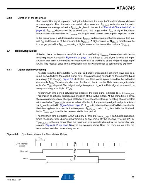
5.4.1 Digital Signal Processing<br />
The data from the demodulator (Dem_out) is digitally processed in different ways and as a<br />
result converted into the output signal data. This processing depends on the selected baud<br />
rate range (BR_Range). Figure 5-8 illustrates how Dem_out is synchronized by the extended<br />
clock cycle T XClk . This clock is also used for the bit check counter. Data can change its state<br />
only after T XClk elapsed. The edge-to-edge time period t ee of the Data signal, as a result, is<br />
always an integral multiple of T XClk .<br />
The minimum time period between two edges of the data signal is limited to t ee T DATA_min .<br />
This implies an efficient suppression of spikes at the DATA output. At the same time, it limits<br />
the maximum frequency of edges at DATA. This eases the interrupt handling of a connected<br />
microcontroller. T DATA_min is to some extent affected by the preceding edge-to-edge time interval<br />
t ee as illustrated in Figure 5-9 on page 16. If t ee is in between the specified bit check limits,<br />
the following level is frozen for the time period T DATA_min = tmin1; if t ee is outside the bit check<br />
limits, T DATA_min = tmin2 is the relevant stable time period.<br />
The maximum time period for DATA to be low is limited to T DATA_L_max . This function ensures a<br />
finite response time during programming or switching off the receiver via pin DATA.<br />
T DATA_L_max is thereby longer than the maximum time period indicated by the transmitter data<br />
stream. Figure 5-10 on page 16 gives an example where Dem_out remains low after the<br />
receiver has switched to receiving mode.<br />
Figure 5-8.<br />
Synchronization of the Demodulator Output<br />
T XClk<br />
Clock bit check<br />
counter<br />
Dem_out<br />
DATA<br />
t ee<br />
4901B–RKE–11/07<br />
15


