ÇUKUROVA UNIVERSITY INSTITUTE OF NATURAL AND APPLIED ...
ÇUKUROVA UNIVERSITY INSTITUTE OF NATURAL AND APPLIED ... ÇUKUROVA UNIVERSITY INSTITUTE OF NATURAL AND APPLIED ...
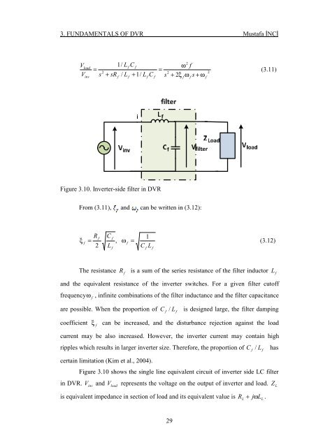
3. FUNDAMENTALS OF DVR Mustafa İNCİ V V load inv 2 = 1/ L f C f ω f = 2 2 s + sR / L + 1/ L C s + 2ξ ω s + ω (3.11) f f f f f f 2 f Figure 3.10. Inverter-side filter in DVR From (3.11), and can be written in (3.12): ξ f = R C f f 2 L f , 1 ω f = (3.12) C L f f The resistance R f is a sum of the series resistance of the filter inductor and the equivalent resistance of the inverter switches. For a given filter cutoff frequencyω , infinite combinations of the filter inductance and the filter capacitance f L f are possible. When the proportion of C / L is designed large, the filter damping f f coefficient ξ f can be increased, and the disturbance rejection against the load current may be also increased. However, the inverter current may contain high ripples which results in larger inverter size. Therefore, the proportion of C / L has certain limitation (Kim et al., 2004). Figure 3.10 shows the single line equivalent circuit of inverter side LC filter in DVR. V inv and V load represents the voltage on the output of inverter and load. Z L f f is equivalent impedance in section of load and its equivalent value is R + jωL . L L 29
3. FUNDAMENTALS OF DVR Mustafa İNCİ The basic principle behind the design of the filter is to provide a shunt path for the harmonic current and a series impedance to carry the harmonic voltages. To achieve this goal, the capacitor should be chosen to satisfy (Choi, et al., 2002): Z = K Z , K >> 1 (3.13) Load ( m) f Cf ( m) f Where Z − j ( m C) ( >> / ω andω 0 = 2πf 0, f0 , represents the fundamental cf m) 0 frequency, and is the order of the lowest harmonics to be attenuated. From Figure 3.10, let V inv(n) and V L(n) represent the respective nth order harmonic voltages on the inverter and load-side of the L-C filter and n=m,m+1,m+2,m+,,,,,M. M is the order of the highest harmonics to be attenuated. By using (3.13), we can obtain the following relationship: V = K V (3.14) load ( n) ( n) inv( n) 2 Where = 1/ ( n ) LC 1) K n ω . Thus, ( ) 0 − 1 1+ K( n) L = (3.15) 2 ( nω ) C 0 From (3.13), it is obvious that for a given Z load , C is directly proportional to K f . Thus, a suitable value for C can be obtained by the selection of an appropriate value for K . Furthermore, (3.14) means that, in order to reduce the nth order f harmonic voltage with rms value from V inv(n) to V load (n) , the inductor of the filter can be chosen according to (3.15) once the capacitor value C is given and K (n) is chosen according to (3.14). Indeed, it will be shown in the next section that the voltage 30
- Page 1 and 2: ÇUKUROVA UNIVERSITY INSTITUTE OF N
- Page 3 and 4: ABSTRACT MSc THESIS MODELING AND AN
- Page 5 and 6: ACKNOWLEDGEMENTS First and foremost
- Page 7 and 8: 3.2.2.1. Inverters ................
- Page 9 and 10: VII
- Page 12 and 13: LIST OF FIGURES PAGES Figure 1.1. D
- Page 14 and 15: Figure 5.3. Injected voltages by us
- Page 16 and 17: LIST OF SYMBOLS C : DC Link Capacit
- Page 18 and 19: LIST OF ABBREVATIONS A AC APF ASD C
- Page 20: 1. INTRODUCTION Mustafa İNCİ 1. I
- Page 23 and 24: 1. INTRODUCTION Mustafa İNCİ 4
- Page 25 and 26: 2. POWER QUALITY Mustafa İNCİ 2.1
- Page 27 and 28: 2. POWER QUALITY Mustafa İNCİ 2.2
- Page 29 and 30: 2. POWER QUALITY Mustafa İNCİ 2.2
- Page 31 and 32: 2. POWER QUALITY Mustafa İNCİ •
- Page 34 and 35: 3. FUNDAMENTALS OF DVR Mustafa İNC
- Page 36 and 37: 3. FUNDAMENTALS OF DVR Mustafa İNC
- Page 38 and 39: 3. FUNDAMENTALS OF DVR Mustafa İNC
- Page 42 and 43: 3. FUNDAMENTALS OF DVR Mustafa İNC
- Page 44 and 45: 3. FUNDAMENTALS OF DVR Mustafa İNC
- Page 46: 3. FUNDAMENTALS OF DVR Mustafa İNC
- Page 51 and 52: 3. FUNDAMENTALS OF DVR Mustafa İNC
- Page 53 and 54: 3. FUNDAMENTALS OF DVR Mustafa İNC
- Page 55 and 56: 3. FUNDAMENTALS OF DVR Mustafa İNC
- Page 58: 3. FUNDAMENTALS OF DVR Mustafa İNC
- Page 61 and 62: 3. FUNDAMENTALS OF DVR Mustafa İNC
- Page 63: 3. FUNDAMENTALS OF DVR Mustafa İNC
- Page 66 and 67: 4. MODELING OF PROPOSED DVR Mustafa
- Page 68 and 69: 4. MODELING OF PROPOSED DVR Mustafa
- Page 70 and 71: 4. MODELING OF PROPOSED DVR Mustafa
- Page 72 and 73: 4. MODELING OF PROPOSED DVR Mustafa
- Page 74 and 75: 4. MODELING OF PROPOSED DVR Mustafa
- Page 76 and 77: 4. MODELING OF PROPOSED DVR Mustafa
- Page 78 and 79: 4. MODELING OF PROPOSED DVR Mustafa
- Page 81 and 82: 4. MODELING OF PROPOSED DVR Mustafa
- Page 83 and 84: 4. MODELING OF PROPOSED DVR Mustafa
- Page 85 and 86: 4. MODELING OF PROPOSED DVR Mustafa
- Page 88 and 89: 4. MODELING OF PROPOSED DVR Mustafa
- Page 90 and 91: 4. MODELING OF PROPOSED DVR Mustafa
- Page 92: 4. MODELING OF PROPOSED DVR Mustafa
- Page 95 and 96: 4. MODELING OF PROPOSED DVR Mustafa
3. FUNDAMENTALS <strong>OF</strong> DVR Mustafa İNCİ<br />
V<br />
V<br />
load<br />
inv<br />
2<br />
= 1/ L<br />
f<br />
C<br />
f<br />
ω f<br />
=<br />
2<br />
2<br />
s + sR / L + 1/ L C s + 2ξ<br />
ω s + ω<br />
(3.11)<br />
f<br />
f<br />
f<br />
f<br />
f<br />
f<br />
2<br />
f<br />
Figure 3.10. Inverter-side filter in DVR<br />
From (3.11), and can be written in (3.12):<br />
ξ<br />
f<br />
=<br />
R<br />
C<br />
f f<br />
2 L<br />
f<br />
,<br />
1<br />
ω<br />
f<br />
=<br />
(3.12)<br />
C L<br />
f<br />
f<br />
The resistance<br />
R<br />
f<br />
is a sum of the series resistance of the filter inductor<br />
and the equivalent resistance of the inverter switches. For a given filter cutoff<br />
frequencyω , infinite combinations of the filter inductance and the filter capacitance<br />
f<br />
L<br />
f<br />
are possible. When the proportion of<br />
C / L is designed large, the filter damping<br />
f<br />
f<br />
coefficient<br />
ξ<br />
f<br />
can be increased, and the disturbance rejection against the load<br />
current may be also increased. However, the inverter current may contain high<br />
ripples which results in larger inverter size. Therefore, the proportion of C / L has<br />
certain limitation (Kim et al., 2004).<br />
Figure 3.10 shows the single line equivalent circuit of inverter side LC filter<br />
in DVR. V<br />
inv<br />
and V<br />
load<br />
represents the voltage on the output of inverter and load. Z<br />
L<br />
f<br />
f<br />
is equivalent impedance in section of load and its equivalent value is<br />
R + jωL<br />
.<br />
L<br />
L<br />
29


