Fine Pitch Flip Chip with Cu Pillar
Fine Pitch Flip Chip with Cu Pillar
Fine Pitch Flip Chip with Cu Pillar

Create successful ePaper yourself
Turn your PDF publications into a flip-book with our unique Google optimized e-Paper software.
IME Proprietary<br />
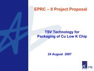
EPRC – 11<br />
Project Proposal<br />
<strong>Fine</strong> <strong>Pitch</strong> <strong>Flip</strong> <strong>Chip</strong><br />
<strong>with</strong> <strong>Cu</strong> <strong>Pillar</strong><br />
9 th November 2010<br />
Slide 1
IME Proprietary<br />
Motivation<br />
• Increasing adoption of <strong>Flip</strong> <strong>Chip</strong> for<br />
mobile application<br />
‣Electrical performance<br />
‣High I/O interconnect<br />
‣Thinner package<br />
‣Cost effective for high pin count<br />
pkg<br />
• <strong>Cu</strong> pillar emerged as solution for fine<br />
pitch flip chip application<br />
‣ Standoff between chip &<br />
substrate<br />
(Source: private communication <strong>with</strong> a wafer foundry )<br />
‣ Avoid solder short<br />
‣ Thermal performance<br />
(Source: Infineon)<br />
Slide 2
Technology Trends<br />
IME Proprietary<br />
(Source: Prismark)<br />
<strong>Cu</strong> pillar bump on commercial microprocessor<br />
<strong>Fine</strong> pitch <strong>Cu</strong> pillar bump on lead substrate<br />
Effect of UF properties<br />
(Source : Amkor)<br />
Slide 3<br />
(Source: <strong>Chip</strong>works)<br />
(Source : Amkor)
Challenges to be Addressed<br />
IME Proprietary<br />
Interconnection<br />
induced<br />
stress on <strong>Cu</strong> low K<br />
structure<br />
• UBM & pillar design<br />
• Low CTE substrate<br />
• UF material<br />
• Reflow process<br />
Reliable joining method and<br />
process issue for fine pitch<br />
<strong>Cu</strong> pillar<br />
• <strong>Pillar</strong> & lead design<br />
• Joining material<br />
• Reflow process<br />
• UF material<br />
Effect of <strong>Cu</strong> pillar Sizes for<br />
different <strong>Pitch</strong><br />
• Routing design rule<br />
• <strong>Pillar</strong> fabrication<br />
• Assembly processibility<br />
• Substrate layout<br />
Electromigration issues<br />
for different <strong>Cu</strong> pillar and joining<br />
material<br />
• <strong>Cu</strong>rrent density distribution<br />
modeling for different pillar size<br />
and joining<br />
• Characterization verification<br />
<strong>Fine</strong> pitch<br />
substrate<br />
• BU (130 -100um)<br />
• 2 layer (50-40um)<br />
Si<br />
Underfilling material,<br />
process and reliability for<br />
fine pitch <strong>Cu</strong> pillar<br />
• Underfill material type<br />
• Underfill process<br />
• Fluxing process<br />
Substrate<br />
Substrate<br />
Challenge<br />
Approach<br />
Test vehicle 1 *<br />
Test vehicle 2 *<br />
Slide 4<br />
• Larger chip**, full array bump<br />
• BU substrate <strong>with</strong> SOP<br />
• <strong>Fine</strong> pitch bump (130um – 100um)<br />
• Low CTE substrate<br />
• Capillary underfill<br />
**Remark: <strong>Cu</strong> low K chip – subject to availability<br />
* To be finalized <strong>with</strong> members input<br />
• Smaller chip**, periphery array bump<br />
• Low cost 2 layer substrate<br />
• <strong>Fine</strong> pitch bump (50um - 40um)<br />
• MUF, WL-UF, NF-UF**<br />
**Remark: To be finalized <strong>with</strong> member’s input and subject<br />
to availability
Project Proposal<br />
Objective:<br />
Development and characterization of fine pitch <strong>Cu</strong> pillar interconnect for next generation devices,<br />
including the following:<br />
IME Proprietary<br />
Structural design and failure mechanism analysis of fine pitch <strong>Cu</strong> pillar for <strong>Cu</strong> low K application<br />
Parasitic extraction, EM modeling and characterization for fine pitch <strong>Cu</strong> pillar<br />
Structural and electrical design rule for fine pitch <strong>Cu</strong> pillar (130um – 40um)<br />
Development of <strong>Cu</strong> pillar <strong>with</strong> different joining method including solder cap, solder bump and <strong>Cu</strong>-<strong>Cu</strong><br />
Material characterization including fine pitch substrate <strong>with</strong> low CTE material and underfill<br />
Assembly, reliability testing and failure analysis<br />
Test vehicle 1 *<br />
Test vehicle 2 *<br />
• Larger chip**, full array bump<br />
• BU substrate <strong>with</strong> SOP<br />
• <strong>Fine</strong> pitch bump (130um – 100um)<br />
• Low CTE substrate<br />
• Capillary underfill<br />
**Remark: <strong>Cu</strong> low K chip – subject to availability<br />
• Smaller chip**, periphery array bump<br />
• Low cost 2 layer substrate<br />
• <strong>Fine</strong> pitch bump (50um /40um )<br />
• Solder cap (SnAg, <strong>Cu</strong>Sn)<br />
• Lead finish (OSP, NiPdAu)<br />
• MUF, WL-UF, NF-UF**<br />
**Remark: To be finalized <strong>with</strong> member’s input and subject<br />
to availability<br />
Slide 5<br />
* To be finalized <strong>with</strong> members input
Improving <strong>Cu</strong> <strong>Pillar</strong> Design for <strong>Fine</strong> <strong>Pitch</strong> Application<br />
IME Proprietary<br />
<br />
Structural modeling and failure mechanism of the<br />
fine-pitch <strong>Cu</strong>-pillar FC package<br />
– <strong>Cu</strong> pillar geometry (e.g. UBM, pillar and landing pad/lead<br />
geometry, etc)<br />
– Packaging materials (e.g. properties of underfill material,<br />
substrate material)<br />
– Bump failure characterization and correlation <strong>with</strong><br />
modeling<br />
– Understanding of failure mechanism / low K delamination<br />
analysis<br />
<strong>Cu</strong> pillar for mechanical/electrical<br />
and routing requirements<br />
<br />
Method for stress reduction for advanced <strong>Cu</strong> low<br />
K device<br />
– Compliant-rigid interconnect structures, including<br />
variable <strong>Cu</strong> pillar e.g. rectangular pillar<br />
– UBM and stress buffering design<br />
– Substrate CTE, landing pad / lead<br />
– Underfill material properties<br />
– Reflow process effect<br />
Slide 6<br />
(Source: IME)
Effect of <strong>Cu</strong> <strong>Pillar</strong> Geometry on<br />
Interconnect Parasitic and <strong>Cu</strong>rrent Distribution<br />
Parasitic extraction<br />
• 3D modeling and experimental characterization the “RLGC” electrical parasitic of the fine<br />
pitch <strong>Cu</strong> pillar (150um 40um) for up to 10 GHz<br />
IME Proprietary<br />
<br />
Electromigration modeling and characterization<br />
• <strong>Cu</strong>rrent density distribution modeling for different pillar size and joining<br />
• Experiment characterization and verification<br />
<br />
<br />
Experimental characterization<br />
• Characterization of RLGC parameters overtime under stressed environmental condition e.g.<br />
temperature and humidity<br />
Design guidelines for fine pitch routing<br />
• <strong>Cu</strong> pillar height, pitch, line width & spacing<br />
• Crosstalk (< -30 dB) , return loss (>10 dB), insertion loss (
Development of Joining Method and Characterization<br />
<strong>with</strong> <strong>Fine</strong> <strong>Pitch</strong> Substrate<br />
<strong>Cu</strong> pillar + solder cap<br />
/ metallic + UF<br />
interconnect<br />
Process development and characterization of different<br />
joining methods<br />
•Comparison of solder cap <strong>with</strong> SnAg, <strong>Cu</strong>Sn, and micro<br />
SnAg bump<br />
•Exploration of <strong>Cu</strong>-<strong>Cu</strong> for fine pitch <strong>Cu</strong> pillar application<br />
• Bonding method (TC, TS, or US)<br />
• Effect of surface finish: SAM coating, NiAu<br />
IME Proprietary<br />
Fabrication for fine pitch <strong>Cu</strong> pillar and substrate<br />
•<strong>Cu</strong> pillar of 130um - 40um bump pitch and AR of >1:1<br />
•<strong>Fine</strong> pitch substrate<br />
• BU substrate (130 -100um pitch)<br />
• 2 layer substrate (50 um - 40um pitch)<br />
• Landing pad / lead sizes, shapes, surface finish<br />
• Low CTE substrate<br />
(Source: JCI)<br />
Slide 8
Assembly Process and Material Characterization,<br />
Reliability Test and Failure Analysis<br />
IME Proprietary<br />
Assembly / process development and characterization<br />
‣ <strong>Fine</strong> pitch <strong>Cu</strong> pillar assembly<br />
‣ Solder cap coplanarity and solder wetting<br />
‣ Selection of flux and solder wetting<br />
‣ Flux dipping process and solder shorting<br />
‣ <strong>Fine</strong> pitch substrate finish (OSP, NiPdAu)<br />
‣ Underfill process characterization<br />
‣ Capillary flow underfill<br />
‣ Wafer level underfill<br />
‣ No-flow underfill<br />
Source: SPIL<br />
‣ Package assembly and sample build for reliability<br />
characterization<br />
Reliability assessment and Failure analysis<br />
‣ Moisture sensitivity test<br />
‣ Temperature cycling test<br />
‣ High temperature storage test<br />
‣ Electromigration test<br />
(Source: Infineon)<br />
Slide 9
Project Flow<br />
IME Proprietary<br />
Members inputs<br />
Finalize project scope /<br />
test vehicle spec<br />
Mechanical/<br />
Electrical<br />
design<br />
Test vehicle design<br />
& wafer fabrication<br />
Solder based <strong>Cu</strong> pillar<br />
assembly development<br />
<strong>Fine</strong> pitch / low CTE<br />
substrate fabrication<br />
Other joining method<br />
development<br />
Experiment<br />
characterization<br />
Quick reliability assessment, material<br />
selection and improvement<br />
Reliability test vehicle fabrication<br />
Slide 10<br />
Final reliability test and FA<br />
Project Time line and schedule : Feb 2011 to Aug 2012
Research Outcome<br />
IME Proprietary<br />
• Design and analysis of <strong>Cu</strong> pillar for fine pitch application<br />
Structural design optimization of <strong>Cu</strong> pillar (pillar, solder, land/lead geometry)<br />
Parasitic and EM analysis of <strong>Cu</strong> pillar<br />
Comparison of <strong>Cu</strong> pillar <strong>with</strong> cap solder and micro SnAg solder bump<br />
Design rule for structural and electrical design of <strong>Cu</strong> pillar (bump pitch 130um – 40um)<br />
• Development of joining method and fine pitch substrate<br />
Process development and characterization results of different joining methods<br />
<strong>Cu</strong> pillar <strong>with</strong> solder cap and micro SnAg solder bump<br />
Exploration of <strong>Cu</strong>-<strong>Cu</strong> fine pitch <strong>Cu</strong> pillar application<br />
Fabrication for fine pitch <strong>Cu</strong> pillar and substrate<br />
<strong>Cu</strong> pillar of 130um- 40um bump pitch and AR of >1:1<br />
Organic substrate <strong>with</strong> 130um - 40um bump pitch<br />
Landing pad / lead sizes, shapes, surface finish<br />
Low CTE substrate<br />
• Assembly characterization, reliability assessment and failure analysis results<br />
Assembly process and characterization of underfill material<br />
Reliability test results<br />
Failure analysis results<br />
Slide 11
IME Proprietary<br />
Thanks for your attention<br />
Slide 12