

mid-end - I-Micronews
mid-end - I-Micronews
mid-end - I-Micronews

You also want an ePaper? Increase the reach of your titles
YUMPU automatically turns print PDFs into web optimized ePapers that Google loves.
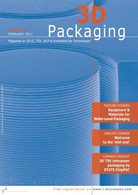
3D<br />
ISSUE N°18<br />
February 2011<br />
Packaging<br />
Magazine on 3D-IC, TSV, WLP & Embedded die Technologies<br />
Printed on recycled paper - (Courtesy of Silex Microsystems)<br />
FEATURE STORIES<br />
Equipment &<br />
Materials for<br />
Wafer-Level-Packaging<br />
ANALYST CORNER<br />
Welcome<br />
to the ‘<strong>mid</strong>-<strong>end</strong>’<br />
COMPANY INSIGHT<br />
3D TSV interposer<br />
packaging by<br />
STATS ChipPAC<br />
F r e e r e g i s t r a t i o n o n www.i-micronews.com
WET DEPOSITION<br />
Superior quality. Lower costs.<br />
Shorter time to market.<br />
Alchimer is a recognized provider of nanometric films for a variety of<br />
microelectronic and MEMS applications, including TSVs for 3D packaging<br />
and wafer-level interconnects.<br />
Our wet deposition technology cuts costs by nearly 80 percent<br />
compared to dry processes, while delivering superior film quality and<br />
shortening time to market.<br />
Contact us to learn how our products deliver a combination of conformality,<br />
step coverage and purity that cannot be matched by dry processes.<br />
We’ll also explain how we can certify new and existing<br />
wet-processing equipment, or provide you with<br />
Alchimer-approved tools and tool suppliers.<br />
alchimer.com<br />
MOLECULES TO BUILD ON
F e b r u a r y 2 0 1 1 I S S U E N ° 1 8<br />
E D I T O R I A L<br />
Advanced Packaging, 2011 expectations<br />
...As the CMOS industry<br />
is transitioning to<br />
32nm and 28nm, wafer<br />
bumping is becoming a<br />
key factor and<br />
an important part<br />
of the supply chain…<br />
Dear readers, 2011 has just started and already appears to be promising dynamic<br />
year. I just recently joined Yole Développement Advanced Packaging team after<br />
several years with TriQuint semiconductor, STMicroelectronics and CEA-LETI.<br />
More recently, I was developing thin film wafer level packaging and flip-chip technology for<br />
SAW filters. Of course, most of the industry is focused on 3D integration with TSV and<br />
especially the new architectures for the new generation of application processors (the “Wide<br />
I/O interface”), but there are lots of initiatives in others domains, like RF-SiP. Being more<br />
focused now on the “big” picture of the packaging industry, it is really interesting to follow the<br />
evolution of the supply chain and how the value is going to be redistributed. By <strong>end</strong> of 2010,<br />
the first 3D with TSV product announcements have been made (Xilinx and Samsung) and<br />
2011 is poised to be a key year for the technology maturation.<br />
This February issue of the 3D Packaging Magazine will focus on the equipment and materials<br />
manufacturers, and the on-going developments in the “<strong>mid</strong>-<strong>end</strong>” infrastructure. 3D TSV,<br />
interposers, FO-WLP or embedded dies are shaking the classical supply chain. At Yole<br />
Développement, we are focused on those new technologies and our role is to understand and<br />
anticipate those changes. For 2011, Yole Développement will release new reports about “3D<br />
IC material and equipment” and “Flip-Chip technology”. The Flip-Chip report will expand our<br />
vision of the advanced packaging supply chain and market, while filling the void in our report<br />
offerings regarding Wafer Scale Packaging Platforms. It is important for us to understand<br />
the Flip-Chip technology and challenges especially as the CMOS industry is transitioning to<br />
32nm and 28nm, wafer bumping (notably lead-free and Cu pillar bumps) is becoming a key<br />
factor and an important part of the supply chain. We are seeing important investments from<br />
the CMOS foundries and the OSAT in order to support this transition. We are following the<br />
main players and their capabilities/capacities worldwide.<br />
Regarding emerging technologies, like FO-WLP, we are tracking the evolution of the<br />
technology (multiple dies, etc…) and the evolution of the manufacturing (transition to panel).<br />
The market share of such technology will be highly dep<strong>end</strong>ing of the infrastructure readiness<br />
and the capabilities of the technology (especially die size and multiple dies).<br />
I hope this issue of 3D Packaging provides new and important information to help you stay<br />
informed about this very dynamic market place.<br />
e v e n t s<br />
• IMAPS - Int. Conf. & Exhibition on Device<br />
Packaging<br />
March 8 to 10, 2011 – Scottsdale, AZ<br />
• DATE 2011<br />
March 14 to 18, 2011 - Grenoble, France<br />
• Semicon China<br />
March 15 to 17, 2011 – Shanghai, China<br />
Dr Christophe Zinck<br />
Project Manager, Advanced Packaging,<br />
Yole Développement<br />
zinck@yole.fr<br />
platinum partners:<br />
3 D P a c k a g i n g 3<br />
For more information, please contact S. Leroy (leroy@yole.fr) or B. Stinson (stinson@i-micronews.com)
F e b r u a r y 2 0 1 1 I S S U E N ° 1 8<br />
C O N T E N T S<br />
Feature Stories – Equipment & Materials 6<br />
Industry Review: 3DICs bring opportunities, challenges<br />
Yole Asks:<br />
• Alchimer on 3D interconnects<br />
• Brewer Science, Inc. leading the world in thin wafer handling solutions<br />
• 3DICs test & metrology: status of the development by FOGALE nanotech<br />
• An interview with Electronics Materials Authority Leo Linehan<br />
• Packaging wafers for MEMS and LED by Plan Optik<br />
Analyst Corner: Welcome to the ‘<strong>mid</strong>-<strong>end</strong>’<br />
Company insight 26<br />
eSilicon: The turning point for MCMs<br />
STATS ChipPAC: Challenges and opportunity in 3D TSV interposer packaging<br />
Notes from Yole Développement 31<br />
Standardization initiatives for 3DICs<br />
Yole Asks 32<br />
IPDiA’s value proposition for interposer products<br />
What’s Inside? 34<br />
SystemPlus Consulting: Silex TSV in MEMS oscillator from Discera<br />
Event Review 36<br />
From i-<strong>Micronews</strong>.com<br />
Stay connected with your peers<br />
on i-<strong>Micronews</strong>.com<br />
W i t h 1 8 , 0 0 0 m o n t h l y v i s i t o r s ,<br />
i-<strong>Micronews</strong>.com provides for Advanced<br />
Packaging area: current news, market<br />
& technological analysis, key leader<br />
interviews, webcasts section, reverse<br />
engineering / costing, events cal<strong>end</strong>ar,<br />
latest reports …<br />
Please visit our website to discover the<br />
last top stories in Advanced Packaging:<br />
• Micron reveals “Hyper Memory Cube”<br />
3DIC Technology<br />
• SPTS wins new 300mm PVD order from<br />
CEA-Leti<br />
• SemiLEDs subsidiar y Helios Crew<br />
launches HB-LED using MEMS silicon<br />
wafer-level-packaging<br />
• 3D Integration Entering 2011<br />
gold partners:<br />
For more information, please contact S. Leroy (leroy@yole.fr) or B. Stinson (stinson@i-micronews.com)<br />
4 3 D P a c k a g i n g
Highlights<br />
• 41 sessions, 36 technical sessions, including 4 poster sessions<br />
and a student poster session<br />
• 16 CEU-approved professional development courses<br />
• Technology Corner Exhibits, featuring approximately<br />
70 industry-leading v<strong>end</strong>ors<br />
• 8 Technical Sessions covering all aspects of 3D/TSV<br />
• Panel Discussion – ECTC Spotlight on China<br />
• Plenary Session – Power Efficiency Challenges and Solutions:<br />
From Outer Space to Inside the Human Body<br />
• CPMT Seminar – Printed Devices and Large Area<br />
Interconnect Technologies for New Electronics<br />
• Special Tuesday Session – The Impact of Manufacturing<br />
Limitations on Electronic Packaging Performance and<br />
Reliability<br />
More than<br />
300 technical papers<br />
covering:<br />
Advanced Packaging<br />
Modeling & Simulation<br />
Optoelectronics<br />
Interconnections<br />
Materials & Processing<br />
Applied Reliability<br />
Assembly & Manufacturing Technology<br />
Electronic Components & RF<br />
Emerging Technologies<br />
Conference Sponsors:
F e b r u a r y 2 0 1 1 I S S U E N ° 1 8<br />
F e a t u r e S t o r i e s – E q u i p m e n t & M a t e r i a l s<br />
Thin Si Wafer on Carrier (Courtesy of EVGroup)<br />
3DICs bring opportunities, challenges<br />
There certainly isn’t a ‘one-size-fits-all’ approach to 3DICs, but it’s a huge business<br />
opportunity with the potential to dramatically shake things up in the semiconductor<br />
industry.<br />
Only a few years ago, the semiconductor industry<br />
was still debating whether or not 3DICs would ever<br />
really take off. But the industry quickly accepted 3D<br />
as a viable path forward—aggressively pursuing it,<br />
finding ways to remove the hurdles, work with the<br />
technology, and actually implement it.<br />
Moving forward, many key decisions must be made<br />
and, as always, there will be more challenges to<br />
maneuver around. Confusion still surrounds the<br />
emerging ‘<strong>mid</strong>-<strong>end</strong>’ area in wafer processing, and<br />
the lack of standardization is also a concern for<br />
many. This time around, the changes aren’t just in<br />
technology: We’re already starting to see signs that<br />
equipment makers will be affected by consolidation.<br />
And since materials will play a pivotal role in the<br />
future of 3DICs and other wafer-level packages, it’s<br />
a good time to also take a look at what’s going on<br />
there and see where they’re headed.<br />
Emerging ‘<strong>mid</strong>-<strong>end</strong>’<br />
With a convergence of front-<strong>end</strong> and back-<strong>end</strong><br />
companies pursuing opportunities in the confusing<br />
zone of overlap in wafer-level packaging between the<br />
back-<strong>end</strong>-of-line (BEOL) and back-<strong>end</strong> packaging,<br />
the term ‘<strong>mid</strong>-<strong>end</strong>’ is now being used to describe<br />
it. This includes not only 3DICs with TSVs, but also<br />
fan-in wafer-level packages, fan-out wafer-level<br />
packages (FOWLP), flip chips, and embedded die.<br />
Not everyone is happy with the usage of this term,<br />
however, because they still see distinctly different<br />
companies with different business models and believe<br />
that front-<strong>end</strong> equipment manufacturers’ move into<br />
the back-<strong>end</strong> has less to do with 3D technology and<br />
more to do with a lack of opportunities in the front<strong>end</strong>.<br />
Regardless, the term ‘<strong>mid</strong>-<strong>end</strong>’ is likely to stick and<br />
gain traction to describe this zone of overlap, as<br />
many companies are seeing this convergence.<br />
6<br />
3 D P a c k a g i n g
I S S U E N ° 1 8 F e b r u a r y 2 0 1 1<br />
“We’re seeing a convergence in the ‘<strong>mid</strong>-<strong>end</strong>’<br />
of the semiconductor industry on multiple<br />
levels,” explains Thorsten Matthias, director<br />
of business development at EV Group.<br />
“Processes and technologies, which used to<br />
be purely front-<strong>end</strong>, back-<strong>end</strong>, or assembly,<br />
are now being moved across all areas. For<br />
example, in the past, oxide wafer bonding was<br />
primarily used for silicon-on-insulator (SOI)<br />
wafer manufacturing, so basically pre-front<strong>end</strong>.<br />
Now it’s used for backside-illuminated<br />
image sensors. And it becomes even more<br />
difficult to distinguish between front-<strong>end</strong>, back<strong>end</strong>,<br />
and assembly when you create a stacked<br />
system such as MEMS-on-ASIC-on-logic. Also<br />
in the <strong>mid</strong>-<strong>end</strong> area, we have a convergence of<br />
industries such as VLSI-ICs, power electronics,<br />
compound semiconductors (CS), and MEMS.<br />
Vertical interconnects and vias have been used<br />
in CS and MEMS for many years.”<br />
In terms of TSVs, both IDMs and OSATs are<br />
pursuing various ‘<strong>mid</strong>-<strong>end</strong>’ types of structures.<br />
“We consider these <strong>mid</strong>-<strong>end</strong> types of structures<br />
to be TSVs between 100 to 200µm deep, with<br />
aspect ratios from 5 to 15,” says Arthur<br />
Keigler, chief technology officer and vice<br />
president of advanced technology at NEXX<br />
Systems. “Most of these are in the range of 100<br />
to 120µm deep, with an aspect ratio between<br />
8 to 10. Lower aspect ratio TSV is being used<br />
now in development mode to take advantage<br />
of existing tool sets by some customers, but<br />
we see movement to higher aspect ratios as<br />
process and tool sets become more affordable.”<br />
In plating, there are also signs of convergence,<br />
bridging IDM/foundry and OSAT, according<br />
to Steve Lerner, CEO of Alchimer SA.<br />
“Unfortunately, we’re not seeing it to the extent<br />
that it should be happening,” he notes. “Litho<br />
requirements are very different for each of the<br />
specified user segments. PCBs and LCDs t<strong>end</strong> to<br />
be panel-driven, while IDM/foundry and OSATs<br />
are solidly wafer-driven. Dry tools typically used<br />
in the front-<strong>end</strong> are trying to make their way<br />
into the OSAT arena, but we feel that approach<br />
is holding back progress because the OSATs<br />
won’t be able to afford such infrastructure.”<br />
The main drivers of the ‘<strong>mid</strong>-<strong>end</strong>’ in 2010 were<br />
flip chip and wafer-level chip-scale packaging<br />
(WLCSP), and it looks like fan-out wafer-level<br />
packaging (FOWLP) may see significant growth<br />
in 2011, followed by 3D TSV technologies in<br />
2013 and beyond.<br />
Front-<strong>end</strong> companies reaching<br />
into the back-<strong>end</strong><br />
We’ve started to see many traditionally ‘front<strong>end</strong>’<br />
equipment companies start pursuing<br />
opportunities in what has been considered,<br />
until very recently, ‘back-<strong>end</strong>’ territory.<br />
3 D P a c k a g i n g<br />
For successful entrance into any market, clear<br />
differentiation must be established, points out<br />
Damo Srinivas, senior director of business<br />
development for Novellus’ equipment portfolio<br />
serving the advanced wafer-level packaging<br />
applications.<br />
“Novellus has introduced several significant<br />
technology advancements to aid in overcoming<br />
challenges associated with TSV integration,<br />
including robust, repeatable TSV fill,<br />
minimization of overburden and wafer bow, and<br />
mitigation of the thermomechanical stability<br />
issues inherent in a copper/silicon system,”<br />
Srinivas elaborates. “Cost, of course, has been<br />
a major hindrance to TSV integration, and<br />
minimizing process time as well as reducing<br />
the cost of consumables are areas Novellus<br />
has innovated. Clearly, with any new market<br />
penetration, platform manufacturability and<br />
reliability are key questions, and our strategy<br />
across our suite of 3D products has been<br />
to heavily leverage our production-proven<br />
productivity-leading front-<strong>end</strong> platforms and<br />
technologies, while optimizing the specific<br />
package for back-<strong>end</strong> integration cost and<br />
technology needs.”<br />
It’s worth noting that there’s a significant<br />
difference in how work is performed in the<br />
front-<strong>end</strong> vs. back-<strong>end</strong>. The back-<strong>end</strong> has<br />
a much greater cost sensitivity and cost<br />
pressures. “You’re forced to take the cost out<br />
of processes very aggressively in the back<strong>end</strong>,<br />
while in the front-<strong>end</strong> it’s more about<br />
ensuring processes work and guaranteeing the<br />
processes and supporting customers with any<br />
issues they may have,” notes Wilfried Bair,<br />
SUSS MicroTec’s vice president of strategic<br />
business development.<br />
The 3DIC market shows the greatest<br />
potential for significant future growth in the<br />
semiconductor industry. It’s a huge business<br />
opportunity, as Bair explains. “How often<br />
does a business opportunity to do something<br />
fundamentally different come along in this<br />
industry? The 3D technology is fundamentally<br />
changing how processing is done and offers the<br />
opportunity for new equipment modifications,”<br />
he says. “Large equipment makers like Applied<br />
or TEL and others in that category or size<br />
typically aren’t interested in anything with<br />
$100-150M equipment revenue, but the 3D<br />
market promises at least several hundred<br />
million for each new product type—so it’s of<br />
great interest.”<br />
Materials development for 3DICs<br />
and other wafer-level packages<br />
Materials will continue to play a pivotal role in<br />
the evolution of 3DICs and other wafer-level<br />
packages. The good news for materials is, as<br />
Phil Garrou, an industry consultant through<br />
his company Microelectronic Consultants of NC,<br />
and also a senior analyst for Yole, puts it: The<br />
process options have narrowed considerably<br />
since 2008, so basically now we’re looking at<br />
‘via-<strong>mid</strong>dle’ processes coming from the fabs<br />
and ‘backside via-last’ most likely coming from<br />
the OSATs, when just two years ago there<br />
were more than 10 process sequences all in<br />
contention.<br />
Along with technical challenges ahead, there<br />
are many other nontechnical, market-driven<br />
issues that need to be addressed, according<br />
to JSR Micro’s Mark Davis, product manager<br />
for packaging materials, and Jim Chung,<br />
program manager in emerging technologies.<br />
They point out that unlike FEOL processes,<br />
for which consortia or alliances pull resources<br />
together to solve technical challenges and<br />
set process development directions, the ‘<strong>mid</strong><strong>end</strong>’<br />
market is much more fragmented and<br />
lacks the needed infrastructure. The result is<br />
smaller, individual companies tackling technical<br />
problems indep<strong>end</strong>ently rather than working<br />
together using common platforms, and the<br />
result is unintentional perpetuation of market<br />
fragmentation.<br />
Not surprisingly, materials are viewed as an<br />
area with great potential for breakthroughs.<br />
“Users are tired of upgrading equipment with<br />
each new generation of products,” says Lerner.<br />
“Material scientists have the opportunity to<br />
create scalable materials that can serve the<br />
Cu Pillars RDL SnAg micro-bumps<br />
More and more key back-<strong>end</strong> realizations are happening at the wafer-level (Courtesy of Novellus)<br />
7
F e b r u a r y 2 0 1 1 I S S U E N ° 1 8<br />
Wafer / Panel Molding<br />
equipments<br />
Equipment & Materials Tool-Box<br />
for 2 nd generation FO WLP manufacturing<br />
Wafer to Wafer Bonding<br />
equipment for 3D stacking<br />
of epoxy wafers<br />
Temporary Bonding / De-<br />
Bonding Handling solution<br />
(equipment & material)<br />
Adhesive material<br />
(Printable paste,<br />
die-attach film)<br />
Yole Developpement<br />
© January 2011<br />
Mold compound<br />
Encapsulant<br />
Exposure & Lithography<br />
(Mask aligners, steppers, LDI…)<br />
Spin coating<br />
Plasma cleaning<br />
(descum, stress relief…)<br />
Wafer test &<br />
Functional test<br />
RDL & Bump<br />
inspection<br />
Chip to foil / Die to<br />
Panel placement<br />
Low-temperature<br />
seed /<br />
metallizations<br />
(PVD / PECVD)<br />
Dielectric passivation<br />
materials (photo-resists,<br />
PCB build-up)<br />
Specific chemistries for:<br />
TMV Electroplating<br />
Surface treatment for better<br />
adhesion of polymer layers<br />
Extracted from Yole Développement’s 2011 report on “Equipment & Materials for the Wafer-Level-Packages”<br />
industry through several generations of design, on<br />
the same equipment platform. This adds value to<br />
the industry in terms of both cost and environmental<br />
impact.”<br />
New materials are under investigation for TSVs,<br />
notes Srinivas. “However, copper electroplating<br />
appears to be the front-runner for the fill, and PVD<br />
seems to be the process of choice for barrier/seed,<br />
both of which are already production proven for<br />
front-<strong>end</strong> applications, and which together tackle<br />
several of the known TSV integration issues such as<br />
thermomechanical robustness,” he adds.<br />
From Davis and Chung’s perspective, examples<br />
of ‘<strong>mid</strong>-<strong>end</strong>’ materials on the horizon that require<br />
further development involve barrier materials such<br />
as ultrathin barrier layers and thermally stable<br />
organic self-assembled barrier materials. They also<br />
believe that interlayer dielectric materials such as<br />
ultralow-k materials and air gaps need work. And for<br />
interconnect conducting materials they expect to see<br />
novel polymers, carbon nanotubes, graphene, and<br />
nanosolders emerge. For encapsulation materials,<br />
they say that desirable qualities include: low CTE,<br />
low modulus, high electrical resistivity, high thermal<br />
conductivity, high moisture resistance, and high<br />
adhesion to materials.<br />
Henkel Electronic Materials LLC is also focusing on<br />
several areas for the ‘<strong>mid</strong>-<strong>end</strong>,’ including advanced<br />
underfill solutions for TSVs and other advanced<br />
flip chip packages or bumped dies, according to<br />
Kevin Becker, Henkel’s director of technology.<br />
“This includes all kinds of pre-applied underfills,<br />
nonconductive pastes, nonconductive films, and<br />
wafer-applied underfill,” he says.<br />
One of the biggest challenges Becker sees is that<br />
the overall assembly process flow has yet to be<br />
determined; it isn’t standardized or even determined<br />
yet. “For materials pre-applied to the wafer, this is<br />
a huge challenge for us. At what point it’s applied<br />
and what processing is done to the wafer after our<br />
material is applied really determines the material<br />
requirements,” he explains. “Process dictates material<br />
properties. For example, the composition of the bond<br />
pads on either side of the substrate or on top of the<br />
bottom die in the stack will have a big impact on the<br />
material properties required for the underfill, whether<br />
it needs to be fluxing, how quickly it needs to cure.<br />
The bonding process will also dictate that, whether<br />
they’re going to use thermal compression bonding,<br />
gravity reflow, ultrasonic, or something else.”<br />
Henkel is heavily involved with materials for<br />
FOWLPs, such as Infineon’s embedded wafer-level<br />
ball grid array (eWLB) technology. “Compression<br />
molding is being used to make ‘virtual’ wafers,<br />
reconstituted wafers, which is a new process to the<br />
market,” explains Becker. “A lot of work is done on<br />
these molded wafers. It’s a somewhat immature<br />
technology; it’s changing very quickly, so the<br />
requirements for compression molding materials are<br />
also changing. The key challenge here, whether it’s<br />
a substrateless package, compression molding for<br />
chip-on-wafer, or other package types, is to manage<br />
the warpage. Molding a 12-inch ultrathin wafer that’s<br />
asymmetric and getting near zero warpage to enable<br />
a dicing process, redistribution process, or stacking<br />
process, is the biggest challenge for that particular<br />
type of package.”<br />
And yes, Becker sees materials that still need to be<br />
developed for 3DICs. He cites underfills, nanofillers,<br />
and backgrinding as being technologies that aren’t<br />
quite ready yet. “There are many temporary bonding<br />
requirements for TSV packages, particularly to enable<br />
mounting of the wafer for various processing, then<br />
8<br />
3 D P a c k a g i n g
I S S U E N ° 1 8 F e b r u a r y 2 0 1 1<br />
easy release afterward,” he says. “I’m sure there are<br />
other issues as well, but the underfill solution and<br />
all of the various temporary bonding adhesives for<br />
backgrinding through dicing and other wafer-level<br />
processing still aren’t there yet.”<br />
Some established companies have the size and<br />
infrastructure to support big customers. When new<br />
technologies come up, it may not always come from<br />
those large established companies, so they buy the<br />
technology and try to force consolidation.<br />
As far as where materials are heading, Becker<br />
believes that graphene certainly has great properties<br />
and won’t be surprised to see big innovations come<br />
out of the technology within the next 3 to 5 years.<br />
He also expects innovations in cure latency and<br />
nanomaterials. Thermal conductivity is another big<br />
issue in 3DICs, particularly if there’s any power or<br />
logic involved, so he hopes to see big innovations in<br />
these and other areas as well.<br />
Standardization<br />
Many in the industry had hoped to see more<br />
processes standardized by now.<br />
There are many reasons for the delay, but as Bair<br />
notes: One is that industry goals, such as those for<br />
TSV diameter, were initially in terms of 15, 20, 25µm,<br />
but R&D groups moved ahead very aggressively<br />
to shrink them to 10µm or smaller. In doing so,<br />
standardization was delayed. “But it brings the<br />
advantages of 3D to products much sooner, because<br />
the smaller vias have less impact on the die area. In<br />
terms of thin wafer handling and temporary bonding,<br />
there wasn’t an expectation that standardization<br />
would occur by now; it’s still a work in progress,” he<br />
explains.<br />
But with all of the announcements about bringing<br />
3DICs to market lately, the lack of standardization<br />
in terms of equipment and processes at this point<br />
is surprising. “It seems like there should be more<br />
maturity in the infrastructure,” says Becker.<br />
Everyone seems to agree that standardization is<br />
still a ways out. “We still have a long way to go in<br />
regard to standardized processes. The 3D pioneers<br />
use a wide variety of integration concepts, process<br />
flows, equipment configurations, processes, and<br />
materials. SEMI recently formed a 3DS-IC standards<br />
committee, with task forces for bonded wafer stacks,<br />
inspection and metrology, and thin wafer handling,”<br />
Matthias says.<br />
Garrou believes that when major players such as<br />
TSMC and Samsung, who are in process qualification<br />
with their major customers right now, are finished<br />
and release their ground rules, it will generate the<br />
materials requirements the industry is searching for<br />
in terms of standardization.<br />
Consolidation ahead<br />
Consolidation is common in semiconductor equipment<br />
companies and we’ve already seen some evidence<br />
of this in the 3DIC arena, namely Applied Materials’<br />
acquisition of Semitool at the <strong>end</strong> of 2009.<br />
3 D P a c k a g i n g<br />
“Another reason behind consolidation is frequently<br />
pressure from markets. For any major investment<br />
into equipment, customers want to ensure that the<br />
supplier has the short-term and long-term capability<br />
to support the installed base and can also ramp the<br />
production volumes quickly enough,” explains Bair.<br />
“And if you take a look at the number of foundries<br />
able to process new technology, it’s constantly<br />
shrinking—and they t<strong>end</strong> to want large equipment<br />
companies to work with and support them.”<br />
Sally Cole Johnson for Yole Développement<br />
Thorsten Matthias is director<br />
of business development at<br />
EV Group headquarters in St.<br />
Florian, Austria. In this role he is<br />
responsible for overseeing EVG’s<br />
worldwide business development.<br />
Matthias received his PhD in technical physics in<br />
2002 from Vienna University of Technology. In his<br />
current role, he works in 3D integration, MEMS,<br />
LED, and nanotechnology.<br />
Steve Lerner is CEO of Alchimer<br />
SA, and a 30-year semiconductor<br />
industry veteran, most notably<br />
fostering emerging technologies<br />
in first level interconnects. He has<br />
held executive positions at startups<br />
Alpha Szenszor, GigaSys, CS2,<br />
and contractors Amkor, Swire, and IMI.<br />
Damo Srinivas is senior director of<br />
business development for Novellus’<br />
equipment portfolio serving the<br />
advanced wafer-level packaging<br />
applications. He received his MS<br />
degree in materials science from<br />
Arizona State University, and a BS degree in<br />
metallurgical engineering from the Indian Institute<br />
of Technology.<br />
Wilfried Bair is SUSS MicroTec’s<br />
vice president of strategic business<br />
development. He is responsible for<br />
developing emerging market and<br />
business opportunities as well as<br />
strategic alliances for SUSS. With<br />
many years of experience working<br />
in 3D technologies and applications, he is focusing<br />
on SUSS’ 3D packaging and 3D integration<br />
product portfolio. Bair is also the general manager<br />
of SUSS’ US organization.<br />
Mark Davis is a product manager<br />
for packaging materials at JSR<br />
Micro. He has 20 years’ experience<br />
in the semiconductor industry in<br />
field applications engineering,<br />
sales, marketing, and product<br />
management.<br />
Phil Garrou is a consultant<br />
in the areas of electronic<br />
materials, IC packaging, and 3D<br />
integration through his company<br />
Microelectronic Consultants of<br />
NC, and a senior analyst for<br />
Yole. Garrou was previously the<br />
global director of technology and new business<br />
development and new business development for<br />
Dow Chemical’s Electronic Business Unit. He is a<br />
fellow of both IEEE and IMAPS, and has served<br />
as president of the IEEE CPMT (2003-2005) and<br />
IMAPS (1997).<br />
James Chung is a program manager<br />
in emerging technologies at JSR<br />
Micro. He holds a BS in chemical<br />
engineering from the University of<br />
Illinois at Urbana-Champaign and<br />
a PhD in physical chemistry from<br />
UCLA. Chung has worked at Intel<br />
in lithography development and at Cheil Industries<br />
(Samsung) in marketing.<br />
Kevin Becker is director of<br />
technology at Henkel Electronic<br />
Materials, LLC, and heads the<br />
Advanced Materials Group as well<br />
as the Film Adhesives Development<br />
Group. He joined Henkel in 1999<br />
and has been responsible for<br />
developing and launching several new product<br />
lines. Most recently he has overseen Henkel’s<br />
launch of the new non-conductive paste preapplied<br />
underfill for fine-pitch copper-pillar-based<br />
applications processors.<br />
Arthur Keigler is chief technology officer,<br />
vice president of advanced technology at<br />
NEXX Systems. He has more than 20 years’<br />
experience in wafer processing, and holds an<br />
MS in materials science and engineering from<br />
MIT, as well as a BS in applied and engineering<br />
physics from Cornell. Keigler was also a Leaders<br />
for Manufacturing Fellow at MIT, earning an MS in<br />
mechanical engineering. He holds several patents<br />
in the field of wafer processing equipment.<br />
9
F e b r u a r y 2 0 1 1 I S S U E N ° 1 8<br />
F e a t u r e S t o r i e s – E q u i p m e n t & M a t e r i a l s<br />
Alchimer on 3D interconnects<br />
CTO Claudio Truzzi discusses the company’s ‘nanotechnology engine’ and low-capex<br />
wet process technology.<br />
Claudio Truzzi,<br />
CTO, Alchimer<br />
Yole Développement: What is the Business<br />
model of Alchimer in the 3D Packaging space?<br />
Claudio Truzzi: Alchimer is offering high<br />
density integration solutions across the entire 3D<br />
interconnect space, starting with high-density<br />
substrates, flexible circuits, BT, LTCC, and right<br />
on through the TSV stack, including isolation,<br />
barrier, seed (if required), and fill. Our films are<br />
sufficiently flexible to address the EMS, OSAT and<br />
IDM/Foundry levels of material processing.<br />
YD: Could you comment about your recent<br />
partnership announcements in Korea and<br />
Japan?<br />
CT: One of Alchimer’s main missions, at this stage<br />
of our growth, is to demonstrate the benefits of<br />
our films in a way that’s regionally and culturally<br />
accessible to our customers. Every substrate<br />
and every design rule is customer-specific, and<br />
deposition processes and materials have to be<br />
tuned to maximize their cost-performance ratio<br />
before integration at the customer site. That’s why<br />
these announcements in Korea and Japan are so<br />
important – they are key to creating the necessary<br />
site synergy in the electronic manufacturing world’s<br />
most strategic regions. We will also be announcing<br />
similar sites in North America and Taiwan, where<br />
customers can utilize local development sites to<br />
tailor our films to their specific needs.<br />
YD: Who is driving the development of 3D<br />
TSV via filling based on Electrografting<br />
technology?<br />
CT: As with all of our products, the market is<br />
driving our via-fill efforts. Originally, Alchimer did<br />
not plan to be in the fill business, as there are so<br />
many competitors. But it became obvious that fill is<br />
a huge bottleneck in many respects. For instance,<br />
Cu Seed<br />
Isolation<br />
purity levels on Cu fill really need to improve to<br />
maximize reliability. Also, the standard group of fill<br />
chemistry suppliers really wasn’t addressing finepitch,<br />
deep-access, bottom-up capabilities. We<br />
feel that by providing clear differentiating products<br />
to address these areas, we can help designers<br />
maximize their real estate and more easily justify<br />
the move to TSV.<br />
YD: What type of equipment can be used to<br />
apply the eG and cG technologies?<br />
CT: Most standard electrolytic and electroless<br />
equipment can be tuned to run our Electrografting<br />
and Chemicalgrafting processes, respectively. The<br />
customer has three options for integrating our<br />
films into a production line:<br />
1. Certified legacy equipment, which a customer<br />
might already own;<br />
2. Inexpensive wet benches and stand-alone ECD<br />
tools, and,<br />
3. Fully automated systems that combine isolation,<br />
barrier, seed and fill, including cleaning, prewetting,<br />
annealing, and other ancillary functions<br />
in one tool with cassette-in, cassette-out material<br />
handling.<br />
This hardware flexibility is one of the most<br />
revolutionary aspects of our technology.<br />
Traditionally, tools have had the leading role in<br />
semiconductor fabs - processes have been toolspecific,<br />
and materials generic. This commonly<br />
accepted approach has brought our industry to<br />
its current juncture, where over-inflated capex<br />
investments are considered a necessary evil.<br />
Alchimer’s wet technology breaks this concept<br />
apart: our unique materials and processes go<br />
hand in hand and are the key to delivering superior<br />
performance for TSV lining and filling. The tool<br />
becomes a mere delivery mechanism, and not a<br />
profit center. This is the essence of how we are<br />
able to provide 60% cost of ownership reduction<br />
in the TSV manufacturing flow (drill, line, fill, CMP).<br />
Barrier<br />
Barrier<br />
SI<br />
Isolation<br />
SI<br />
Top view of a full isolation/ barrier/seed stack on TSV<br />
using wet-deposition technology (Courtesy of Alchimer)<br />
Highly conformal wet Isolation and Barrier<br />
layers on a 4-µm TSV (Courtesy of Alchimer)<br />
10<br />
3 D P a c k a g i n g
I S S U E N ° 1 8 F e b r u a r y 2 0 1 1<br />
YD: Yole Développement recently observed<br />
that two types of 3D Glass & Silicon<br />
interposers are emerging: one type of<br />
interposer is “Front-<strong>end</strong>” oriented, with<br />
small Vias diameters, manufactured in<br />
the CMOS wafer foundry environment.<br />
The second type of interposers is more<br />
“Back-<strong>end</strong>”, with thicker vias, bigger<br />
volume to plate, higher aspect ratios:<br />
could you comment on the benefits eG<br />
technology can bring in such two distinct<br />
types of interposer environments?<br />
CT: Alchimer’s TSV technology is applicationagnostic.<br />
This stems directly from our<br />
basic nanotechnology engine: our films are<br />
chemically bonded onto the wafer and grow<br />
from the surface out, rather than being<br />
deposited onto it. As a direct consequence,<br />
conformality, adhesion and uniformity are<br />
integral to the film layers we produce, and<br />
are not a function of surface topography or<br />
tool performance. We can graft our films<br />
on 1-micron diameter vias as easily as<br />
200-micron vias, with aspect ratios as high<br />
as 30:1.<br />
So, whether your interposer is front-<strong>end</strong> or<br />
back-<strong>end</strong> oriented, glass or silicon-based,<br />
you benefit from the excellent step coverage<br />
and adhesion, lower parasitic capacitance,<br />
higher breakdown voltage, and reduced wafer<br />
bulk stress and copper pumping. And from<br />
an integration perspective, Alchimer’s wet<br />
technology is fully compatible with standard<br />
fab safety and environmental requirements<br />
for handling and waste treatment.<br />
Cu<br />
Barrier<br />
Isolation<br />
Si<br />
Top and bottom view<br />
of a wet-processed,<br />
seedless 3X30 µm<br />
Cu-filled TSV.<br />
Wet isolation<br />
thickness:<br />
top = 80nm;<br />
bottom = 60nm<br />
Wet barrier<br />
thickness:<br />
top = 50nm;<br />
bottom = 35nm<br />
Step coverage >70%<br />
(Courtesy of Alchimer)<br />
YD: According to you, who is the best<br />
3DIC builder: CMOS foundries, OSATs,<br />
MEMS players, PCB substrate houses?<br />
CT: It dep<strong>end</strong>s. We’re using a single term,<br />
3DIC, to indicate very different applications<br />
and technology variations; this often happens<br />
in the early stages of process revolutions.<br />
Today we are seeing more-articulated 3DIC<br />
technology diversification, compared to just<br />
a few years ago, with different options being<br />
selected for different applications. Vertical<br />
connections and chip-stacking requirements<br />
for some applications, such as MEMS devices,<br />
are different from those for memory-on-logic<br />
or for memory stacks.<br />
The point at which the TSV wafer leaves the<br />
fab is a key differentiating factor that can<br />
help categorize the current multitude of 3DIC<br />
process flows. Once that wafer leaves the<br />
fab, it will almost certainly never go back.<br />
The number and type of steps the wafer<br />
still needs to undergo after that point (in<br />
the post-fab portion of the process flow) are<br />
determined by the application.<br />
3 D P a c k a g i n g<br />
For a single-device memory stack, the postfab<br />
portion is minimal - the fab will own the<br />
majority of the 3DIC flow. For an interposer<br />
with a memory stack on one side and a<br />
microprocessor on the other, the post-fab<br />
portion may be considerably larger and OSATs<br />
have the opportunity to own a larger portion<br />
of the flow. It’s worth noting that the current<br />
capex and dry-process know-how required for a<br />
full 3DIC line may represent a major barrier to<br />
entry for OSATs. Alchimer’s solution, based on<br />
low-capex wet process technology, can address<br />
that.<br />
www.alchimer.com<br />
Claudio Truzzi, CTO, Alchimer<br />
CTO Claudio Truzzi joined Alchimer with more<br />
than 20 years of experience in R&D, engineering,<br />
manufacturing, and product development in the<br />
microelectronics industry. His expertise encompasses<br />
molecular engineering, 3D-IC process flows,<br />
IC design, microelectronic packaging, MEMS<br />
and bio-electronic components, box build, wireless<br />
systems and hardware/software integration.<br />
Claudio’s achievements include development<br />
of miniature high-performance electronic<br />
systems for wireless and industrial applications,<br />
high-frequency packaging, antennas and filters,<br />
and wireless sensor networks.<br />
Earlier in his career he consulted with<br />
electronic-manufacturing services companies,<br />
semiconductor equipment manufacturers, waferlevel<br />
process developers, and optoelectronics<br />
companies. He also has held senior management<br />
positions at Convergix and CS2 in Europe.<br />
Widely published in scientific journals and conference<br />
proceedings, Claudio has an M.S. degree in<br />
electronic engineering from the University of Bologna<br />
and a Ph.D. degree in electronic engineering from the<br />
University of Torino.<br />
11
F e b r u a r y 2 0 1 1 I S S U E N ° 1 8<br />
F e a t u r e S t o r i e s – E q u i p m e n t & M a t e r i a l s<br />
Brewer Science, Inc. leading<br />
the world in thin wafer handling<br />
solutions<br />
Dan Wallace<br />
Director of Advanced<br />
Packaging SBU<br />
Brewer Science Inc.<br />
Yole Développement: Dan, you started with<br />
Brewer Science in 2008. How about a little<br />
background on what you were doing before<br />
you joined Brewer Science and what your<br />
current role there is?<br />
Dan Wallace: I started in the industry in 1981,<br />
so I certainly have seen many advancements.<br />
Most of my career was with Motorola, and I later<br />
moved to Freescale Semiconductor when Motorola<br />
spun off their semiconductor products group. With<br />
Motorola and Freescale I was involved in a broad<br />
range of positions such as R&D, manufacturing,<br />
product management, marketing, and business<br />
management. When I left Freescale to join Brewer<br />
Science, I was the operations manager for the<br />
MEMS Pressure Sensor Business Unit.<br />
Now in my position at Brewer Science as the<br />
Director of the Advanced Packaging Business Unit,<br />
I find that this experience has given me a unique<br />
vantage point in understanding many of the<br />
challenges our customers face.<br />
YD: Brewer Science, Inc., is a 30-year-old<br />
company with headquarters in Rolla, Missouri.<br />
Can you give us a little background on how the<br />
company started?<br />
DW: Brewer Science is a privately held specialty<br />
chemical company founded in 1981 by Dr. Terry<br />
Brewer and headquartered in Rolla, Missouri.<br />
Brewer Science delivers materials, processes, and<br />
equipment for applications in semiconductors,<br />
advanced packaging/3-D ICs, MEMS, displays, LEDs,<br />
and printed electronics.<br />
Everything about the company is unique, from the<br />
fact that it’s a high-tech company located in rural<br />
Rolla, Missouri, to its 30-year history of consistent<br />
and successful global growth. Brewer Science’s<br />
open-minded approach to customer needs and indepth<br />
knowledge of process technologies has helped<br />
it to grow to be a global company with employees<br />
and offices in Asia, Europe, and North America<br />
supporting a worldwide customer base.<br />
The company’s vision and commitment is focused<br />
on introducing innovative technology solutions for<br />
the ever changing needs of the microelectronics<br />
industry.<br />
YD: We have seen that Brewer Science<br />
recently opened new offices in Tokyo, Japan,<br />
and Seoul, Korea, to go along with offices in<br />
Taipei, Shanghai, and Hong Kong. Are these<br />
sales offices? How do you handle “field<br />
engineering” for customers? Do you have<br />
engineers stationed in Asia? Or are technical<br />
issues dealt with from the US?<br />
DW: Brewer Science is purposefully executing<br />
a long-term strategy of developing more local<br />
support in the regions where we continue to see<br />
growth. The type of support will dep<strong>end</strong> upon the<br />
needs of that specific region, although in most<br />
cases we are installing sales and some level of field<br />
applications support with US applications always<br />
very much involved. It would be important to note<br />
that Brewer Science has made a considerable<br />
investment in Taiwan by opening up an applications<br />
lab in early 2009. Already the size of the lab has<br />
doubled, and it continues to install equipment in<br />
support of Brewer Science products. As of today,<br />
the Taiwan lab is supporting a significant portion of<br />
our applications work in Asia.<br />
Thin Wafer BSI (Courtesy of Brewer Science)<br />
YD: A little introduction to your main product<br />
lines is probably in order. Brewer Science<br />
is probably best known for its ARC ® antireflective<br />
coating products used in the<br />
microlithography world. Please give us a bit<br />
of a description of your main product families.<br />
DW: After inventing anti-reflective coatings 30 years<br />
ago in 1981, Brewer Science’s continuing approach is<br />
to create and deliver innovative, originally developed<br />
materials and process solutions that enable a<br />
variety of microelectronic processes and allow a<br />
competitive edge for our customers. We make a<br />
significant investment in R&D, which is apparent<br />
12<br />
3 D P a c k a g i n g
I S S U E N ° 1 8 F e b r u a r y 2 0 1 1<br />
Latest Solution - ZoneBOND<br />
Room temperature debond process<br />
(Courtesy of Brewer Science)<br />
Device<br />
Carrier<br />
1<br />
2<br />
Adhesive on Device<br />
3<br />
Device<br />
Polymer Adhesive<br />
Carrier<br />
4<br />
ZB Carrier<br />
Release Zone<br />
Stiction Zone<br />
Thin Device<br />
Basic Process Flow:<br />
1. Coat polymer adhesive on Device<br />
2. Create carrier: (Release Zone & Stiction Zone)<br />
3. Bond face to face<br />
4. User processes, thin, pattern, etc.<br />
5. Remove stiction zone adhesive<br />
6. Mount device wafer to film frame & vacuum<br />
chuck - Peel Carrier from adhesive<br />
7. Clean adhesive from Device while on film frame<br />
5<br />
6<br />
7<br />
given the leadership role we play in the industry.<br />
Brewer Science has commercial products and<br />
developmental activities focused in the areas<br />
of lithography, LEDs, solar applications,<br />
MEMS, carbon nanotubes, printable/flexible<br />
electronics, and advanced packaging. As<br />
far as specific products, Brewer Science<br />
continues to expand its scope with CNTRENE ®<br />
microelectronics-grade carbon nanotube<br />
solutions, ProTEK ® temporary etch protective<br />
coatings, WaferBOND ® temporary bonding<br />
materials, ZoneBOND low-temperature<br />
debonding system, OptiNDEX high refractive<br />
index coatings, and Cee ® benchtop laboratory<br />
processing equipment.<br />
I would like to mention that Brewer Science<br />
really identifies a product in much broader<br />
terms beyond a bottle of polymer or a piece<br />
of equipment. The value that Brewer Science<br />
offers is the ability to deliver solutions to the<br />
industry based on our 30 years of experience.<br />
These solutions will include not only innovative<br />
materials but also our equipment and process<br />
experience.<br />
YD: Certainly i-<strong>Micronews</strong> readers are<br />
all aware of the WaferBOND ® temporary<br />
bonding products. It’s been clear that<br />
Brewer Science was the first chemical<br />
company to understand the need for<br />
temporary adhesives. Was this the<br />
result of your membership in EMC-3D<br />
consortium in 2007 or were you aware<br />
of these needs earlier?<br />
DW: Brewer Science was aware of the coming<br />
opportunity much earlier and started working<br />
on temporary bonding in 2003. We launched<br />
our first temporary bonding material, a<br />
WaferBOND ® product, in 2006. Since that<br />
time we have introduced several improved<br />
temporary bonding materials in support of the<br />
high-temperature slide debonding process.<br />
More recently, Brewer Science has introduced<br />
our patented ZoneBOND technology, which<br />
was developed to solve many of the industry<br />
problems with existing thin wafer handling<br />
processes.<br />
In addition, Brewer Science has authored over<br />
20 publications and has been issued over 70<br />
US and international patents related to 3D<br />
technology, which has further positioned<br />
Brewer Science as a market leader for this<br />
technology.<br />
YD: We have heard that there are<br />
now several grades (differentiated by<br />
temperature stability and removal<br />
temperature) of WaferBOND ® products<br />
available. Can you elaborate?<br />
DW: I first should talk about our temperature<br />
ratings of materials. For lack of a better<br />
method, we have chosen to assign a value<br />
representing the temperature capability or<br />
tolerance of that adhesive. For example,<br />
we say our WaferBOND ® HT10.10 product<br />
is a 220°C material. This description is very<br />
general because the overall capability of the<br />
material is dep<strong>end</strong>ent on not only the back<strong>end</strong><br />
processing temperatures but also on<br />
many other factors that influence how well<br />
the material will perform during back-<strong>end</strong><br />
processing. These factors include time at<br />
temperature, the presence of a vacuum or<br />
pressure environment, energy level such as<br />
in a PECVD process, and the degree of wafer<br />
stress at elevated temperature. Dep<strong>end</strong>ing<br />
on these factors we have seen WaferBOND ®<br />
HT10.10 material performs well at 250°C and<br />
in other cases fails at 200°C. Our development<br />
efforts have taught us that all related process<br />
factors must be well understood.<br />
WaferBOND ® HT10.10 material is our current<br />
commercially released product. At the same<br />
time, we are also working on several new<br />
advanced platforms of adhesives targeted for<br />
temperature capabilities of up to 300°C. We<br />
have chosen to work with key customers in<br />
the development of these materials to ensure<br />
our developmental goals align well with our<br />
customers’ needs.<br />
YD: Since the 3D IC market has been<br />
“coming soon” for a few years now, how<br />
does a moderate-sized company such as<br />
Brewer Science decide on the appropriate<br />
investment level for such leading-edge<br />
technology developments? Did you get in<br />
too early? or was your timing just right?<br />
DW: Your question is a very interesting one,<br />
and I am sure on where every company has<br />
experienced both scenarios. If we could<br />
accurately predict when a new technology such<br />
3 D P a c k a g i n g<br />
13
F e b r u a r y 2 0 1 1 I S S U E N ° 1 8<br />
as 3D IC may launch, we would rule the world.<br />
More often, that is not the case. It is Brewer<br />
Science’s focus to invent and provide cuttingedge<br />
technology solutions, and entering the<br />
3D IC market was a result of following this<br />
approach. Some of our methods may be<br />
more confidential in nature, but, in general,<br />
to aid in reducing the risk, we work closely<br />
with key suppliers and customers throughout<br />
the supply chain. These relationships have<br />
been instrumental in helping Brewer Science<br />
to determine the level of investment versus<br />
when a new technology may launch. Entering<br />
as early as we did has helped us in developing<br />
broader relationships in the industry and in<br />
understanding the applications much better<br />
than any of our competition. In that respect, I<br />
believe our timing was just right.<br />
YD: Does being a <strong>mid</strong>-sized chemical<br />
company give you any advantages over<br />
the “big boys”?<br />
DW: I find that, overall, we move faster.<br />
Communication is much easier because 90%<br />
of the company is within the same campus,<br />
so most of our colleagues are a 5-minute<br />
walk away. In addition, our processes foster<br />
close connections with our global employees.<br />
Usually decisions are made in hours rather<br />
than weeks or months. Our customers also<br />
recognized that because we are a <strong>mid</strong>sized<br />
company we have greater flexibility in<br />
responding to their current technology needs<br />
and developing innovation that will address<br />
future challenges.<br />
YD: Since most 3D customers clearly<br />
want an “equipment + materials” tested<br />
solution for their thin wafer handling<br />
needs, your relationship with EVG has<br />
certainly helped introduce your material<br />
solutions to the industry. How has that<br />
developed through the years?<br />
DW: Brewer Science and EV Group<br />
early on recognized that the solution for<br />
temporary wafer bonding will not be just<br />
material or equipment alone, but it will be<br />
the combination of both working together.<br />
Given this, we have made much progress<br />
over the years advancing the development<br />
of temporary bonding technology. Now as<br />
the industry is coming closer to actually<br />
launching 3D IC technology, it is key for<br />
the market to have multiple suppliers in<br />
order to meet the demand and continue<br />
innovation. Thus Brewer Science continues<br />
to work with EV Group in the marketing of<br />
high-temperature slide debonding equipment<br />
and materials, but we are also pursuing a<br />
non-exclusive path with multiple equipment<br />
suppliers on newer technology, such as the<br />
Brewer Science ZoneBOND process.<br />
YD: We’ve seen recently that Suss Microtec<br />
is also offering a “WaferBONDlike” solution<br />
for its bonder/debonder equipment line.<br />
Care to discuss your relationship with<br />
Suss?<br />
DW: As mentioned above, we are pursuing<br />
a non-exclusive path with multiple equipment<br />
suppliers on technologies such as WaferBOND ®<br />
and ZoneBOND technologies. Ultimately we<br />
see this as the best way to serve the market<br />
needs and drive further innovation in both<br />
equipment and material development.<br />
YD: The EMC-3D consortium appears to<br />
be winding down. Care to comment on how<br />
membership in this consortium affected<br />
your overall 3D business strategy?<br />
DW: We benefited in several ways from the<br />
relationship. Certainly the combined process<br />
evaluation work of the membership was<br />
extremely beneficial. I would also say the<br />
work put into the CoO model was a good<br />
experience. Even though some of the input<br />
data may still need to be refined, the baseline<br />
model will prove to be a useful tool for the<br />
industry.<br />
YD: Being out there on the front line of 3D<br />
IC you certainly must have a perspective<br />
on how much longer it will be until we see<br />
real product-driven commercialization.<br />
What’s your best guess?<br />
DW: I think we all recognize from conferences<br />
and direct customer partnerships that we will<br />
see launches starting in 2012 to 2013. These<br />
may be slow at first while the main concerns<br />
are still being resolved. But as the industry<br />
begins to resolve the major concerns and the<br />
volumes help drive down the costs, I believe<br />
the benefits of 3D IC will drive a whole new<br />
market and level of performance.<br />
YD: We saw that you created a research<br />
collaboration with CEA Leti in 2009.<br />
What was that about, is it still in place,<br />
and how has that worked out?<br />
DW: We continue to work with Leti, with our<br />
efforts focused on evaluating developmental<br />
temporary bonding material performance<br />
through various backside processes and<br />
related process development, such as<br />
coating, bonding, debonding, cleaning, etc. I<br />
think we would all agree that the relationship<br />
has been very valuable.<br />
YD: The latest 3D based technology we<br />
have seen from Brewer Science is the<br />
“Zonebond Process.” Can you give us a<br />
short description and status report?<br />
DW: A picture is worth a thousand words.<br />
The scheme on the previous page describes<br />
the process pretty well. The motivation in<br />
developing a process technology such as<br />
ZoneBOND was driven by the desire to<br />
solve several key customer concerns with<br />
the existing thin wafer handling technologies.<br />
Overwhelmingly, our goal was to develop a<br />
solution that would offer maximum protection<br />
to the thinned device wafer, enable the<br />
use of value-added materials with a higher<br />
temperature tolerance, and lower the overall<br />
CoO by increasing throughput for both<br />
bonding and debonding. Based on results to<br />
date, I am confident that we will deliver such<br />
a solution.<br />
YD: Any other new products coming<br />
through the pipeline that our readers<br />
should be aware of?<br />
DW: I would love to share that information<br />
with you, but until we are closer to<br />
commercialization such activities are of a<br />
confidential nature. All I can say is that we<br />
continue to invest a significant percent of<br />
revenue in developmental activity aimed at<br />
new disruptive technologies that will enhance<br />
existing processes and expand capability to<br />
address existing and new applications for the<br />
microelectronics industry.<br />
www.brewerscience.com<br />
Dan Wallace<br />
Director of Advanced Packaging SBU Brewer<br />
Science Inc.<br />
Dan has been in the electronics industry for over<br />
twenty-nine years working in diverse and progressive<br />
roles in device design, manufacturing engineering,<br />
marketing and business development. His current<br />
focus is on material and business development for<br />
advanced material and process solutions in the area of<br />
thin wafer handling for 3DIC packaging applications.<br />
Dan’s background spans a broad range of<br />
technologies including, Power MOSFET, custom Analog<br />
IC’s, and MEMS products for the automotive market<br />
place. He has a masters in business, bachelors in<br />
electrical engineering and is a certified black belt in<br />
LEAN/Six-Sigma practices for manufacturing and<br />
business processes. Dan has authored several papers,<br />
patents and has spoken at various conferences.<br />
14 3 D P a c k a g i n g
I S S U E N ° 1 8 F e b r u a r y 2 0 1 1<br />
F e a t u r e S t o r i e s – E q u i p m e n t & M a t e r i a l s<br />
3DICs test & metrology:<br />
status of the development<br />
by FOGALE nanotech<br />
Yole Développement met the company FOGALE nanotech, the reference in the field<br />
of high accuracy dimensional metrology. Discover below the exchange between the<br />
consulting company and FOGALE: overview of FOGALE solutions, FOGALE’s point<br />
of view on the test & metrology developments, feedback on the status of the 3DICs<br />
industry…<br />
Yole Développement: Could you introduce us<br />
about Fogale Nanotech’s activity and company<br />
background?<br />
Gilles Fresquet: FOGALE nanotech, a company<br />
created in 1983, is now a worldwide known reference<br />
in the field of high accuracy dimensional metrology.<br />
FOGALE Nanotech headquarter is located in Nîmes,<br />
south of France, with two subsidiaries located in the<br />
USA and in Taiwan.<br />
Back in the 80’s and the 90’s, FOGALE nanotech<br />
provided metrology solutions for big scientific<br />
instruments such as Very Large Telescopes,<br />
nuclear reactors, particle accelerators and medical<br />
instruments. As an example, all the main particle<br />
accelerators are equipped with FOGALE sub<br />
micrometer leveling systems (capacitive method)<br />
and very large telescopes with FOGALE focus<br />
adjustment devices based on interferometry and<br />
optical techniques. Amazingly, the physics laws of<br />
the developed non contact metroly solutions for<br />
particle accelerators and very large telescopes are<br />
the same than the one used to monitor life cells or<br />
silicon wafers. So, since <strong>mid</strong> 90’s, FOGALE nanotech<br />
is delivering systems for the biotech, optical and<br />
semiconductor applications.<br />
With a high level of expertise in optical metrology<br />
and a strong scientific background, FOGALE<br />
nanotech provides tools well suited to new<br />
metrology requirements in the 3D integration and<br />
MEMS process control. FOGALE nanotech was the<br />
first company able to deliver metrology solution for<br />
MEMS in motion optical analysis and optical analysis<br />
of devices under controlled atmosphere.<br />
Since 2007, FOGALE R&D team is focusing on<br />
metrology and inspection solutions for the 3DIC &<br />
TSV area.<br />
YD: Can you comment on the recent traction you<br />
are seeing in the 3DIC & TSV metrology area?<br />
What needs to be measured and inspected for<br />
3DICs as of today?<br />
GF: FOGALE nanotech is currently involved in several<br />
projects concerning 3D integration. Through a joint<br />
development program with imec, the TSV depth<br />
measurement system (Deeprobe) has been qualified<br />
for Via first or <strong>mid</strong>dle process control. The goal was<br />
to measure the 25 to 50 µm depth of 5µm diameter<br />
TSV with good accuracy, linearity and repeatability.<br />
The Deeprobe has been lately used to measure 2µm<br />
diameter TSV with 1:25 Aspect Ratio on 300mm<br />
wafers.<br />
FOGALE nanotech is also involved in other projects<br />
concerning Via last approach for 3D integration. We<br />
are working with academics and industrial partners<br />
such as IEF (Institute of Fundamental Elelectronics<br />
Orsay), ST, LETI and others. The implementation<br />
of a common lab FOGALE-CNRS (French National<br />
Research and scientific Center) is ongoing.<br />
FOGALE is involved in the SMARTSTACK project<br />
(Partners: CEA LETI, ST micro, TEGAL FRANCE,<br />
“IDMs are very<br />
aggressive in the<br />
3DIC development<br />
but OSATs and<br />
CMOS foundries<br />
are not far behind,<br />
they want<br />
to be ready,”<br />
says Gilles Fresquet,<br />
FOGALE nanotech<br />
3 D P a c k a g i n g<br />
Fogale headquarter<br />
Fogale Laboratory (Courtesy of Fogale nanotech)<br />
15
F e b r u a r y 2 0 1 1 I S S U E N ° 1 8<br />
“For all technologies,<br />
low cost and fast<br />
measurement<br />
methods will<br />
be required,”<br />
comments<br />
Gilles Fresquet<br />
41,4<br />
Die to wafer process stacking: Smartstack Project<br />
(Courtesy of Fogale nanotech)<br />
Ecoles des mines de St Etienne and GEMALTO). The<br />
goal of this project is to deliver a 3D platform able to<br />
combine several dies for several applications.<br />
5 major items are studied within this 3 years<br />
program:<br />
• Deep RIE process tuning to obtain optimal TSV<br />
structures.<br />
• Interconnect process for die to die and die to wafer<br />
connection.<br />
• Thinning processes for final 40 to 60 µm thick<br />
silicon wafers.<br />
• Modeling of several 3D integration schemes and<br />
validation by reliability test.<br />
• Performances study of the developed 3D modules.<br />
Within the smartstack project, FOGALE is in charge<br />
to deliverall the required in line process control<br />
solutions for all process steps (from TSV, thinning<br />
to final 3D interconnection). FOGALE is also working<br />
on metrology solutions for reliability studies. Thanks<br />
to the global approach of the smartstack project, a<br />
first tool has been designed and delivered for TSV<br />
control and wafer thinning process inspection. The<br />
FOGALE approach always combines microscopy and<br />
metrology, and this tool can also be used to monitor<br />
the final 3D interconnect process step.<br />
Today, for 3D ICs , several process steps need to be<br />
controlled:<br />
• TSV: depth, profile, liner integrity, voids after fill etc..<br />
• Thinning: post bonding inspection to detect<br />
defects at the interface between the wafer and<br />
the temporary carrier, Total Thickness Variation of<br />
the glue layer. After back grind, apart from Silicon<br />
thickness which is required, edge and backside<br />
defects must be detected.<br />
• Interconnect: Non contact metrology and inspection<br />
solutions are required to control the interface and<br />
the alignment between dies and copper nails height<br />
and co-planarity.<br />
• Reliability and performance: Metrology and<br />
inspection solutions to avoid failures due to<br />
mechanical stress and environmental parameters<br />
and control solutions for the final package.<br />
YD: Could you comment on the different<br />
3DIC metrology & inspection methods today<br />
available and their related benefits (Moiré<br />
interferometry, X-Ray, SAM, others…)?<br />
GF: Several technologies can be used to control 3DIC<br />
process steps.<br />
• To measure substrate thicknesses, we can use<br />
capacitive or optical technologies. The advantage<br />
of optical technologies is the capability to measure<br />
multi layer substrates such as Si on temporary<br />
carrier.<br />
• For Substrate flatness, optical methods such as laser<br />
scanning, confocal chromatic or interferometry are<br />
working well. For surface roughness after thinning,<br />
AFM or optical techniques can be used. However<br />
optical techniques are preferred if a measurement<br />
on a large area is required.<br />
• For high A/R TSV, the SEM is used on cross section<br />
but it is a destructive method so a non contact<br />
measurement is required. Full field interferometry<br />
can be used but is limited to low A/R. Confocal and IR<br />
interferometry are the best candidates for high A/R<br />
TSV. However, after backgrind, IR interferometry is<br />
also able to measure Remaining Silicon Thickness<br />
over copper nails. For TSV characterization, the<br />
X-Ray tomography is the perfect solution for<br />
measurement on small samples.<br />
• For post bonding inspection, full wafer optical<br />
methods are working well, both in reflection or<br />
transmission.<br />
TSV depth uniformity across a 300 mm wafer (TSV diameter : 5 μm)<br />
Measurement done with FOGALE DeeProbe 300 (Courtesy of imec)<br />
41,2<br />
Via Depth (μm)<br />
41<br />
40,8<br />
40,6<br />
40,4<br />
40,2<br />
40<br />
39,8<br />
X position across a 300mm wafer diameter (mm)<br />
16 3 D P a c k a g i n g
I S S U E N ° 1 8 F e b r u a r y 2 0 1 1<br />
• For the die interconnect, the IR interferometry<br />
combined with NIR microscopy is a good candidate<br />
for in line process control. X-Ray tomography<br />
and acoustic microscopy are used but mainly for<br />
characterization.<br />
• For hermetic package characterization, we can<br />
use mass spectrometry, IR spectrometry and<br />
Raman spectrometry. For wafer level packaging,<br />
IR interferometry with NIR microscopy is a good<br />
non destructive solution and can be used on a full<br />
wafer surface.<br />
YD: 3DIC inspection & metrology is today<br />
clearly a booming area but mainly remains in<br />
the R&D and laboratory space. According to<br />
you, which inspection, metrology and testing<br />
steps for 3DICs may be finally integrated “inline”<br />
into high volume production?<br />
GF: I’m convinced that TSV and wafer thinning<br />
process control solutions will be integrated into high<br />
volume production. For 3D interconnect step, it will<br />
dep<strong>end</strong> a lot on the 3D process integration approach.<br />
There are so many different ways to do it.<br />
In all cases, low cost and fast measurement methods<br />
will be required. We still miss versatile and fast<br />
solutions for in line process controls. Inspection and<br />
metrology on the same platform is a good approach.<br />
www.fogale-semicon.com<br />
YD: Who is the most aggressive in the<br />
development of test and metrology solutions<br />
for 3DICs based on TSV: OSATs, IDMs or CMOS<br />
Foundries?<br />
GF: FOGALE is working with all the players. IDMs are<br />
very aggressive in the 3DIC development but OSATs<br />
and CMOS foundries are not far behind, they want to<br />
be ready. The question about the timing dep<strong>end</strong>s on<br />
the final applications for 3DICs.<br />
Gilles Fresquet is the manager of the semiconductor<br />
business at FOGALE Nanotech. Before joining FOGALE,<br />
Fresquet spent many years at Thomson, Motorola<br />
and RECIF in a variety of process engineering and<br />
management roles. He hold a MSc. In Physics and has<br />
more than 25 years of semiconductor experience.<br />
F a b r i c a t i o n E q u i p m E n t F o r t h E i n t E g r a t E d c i r c u i t i n d u s t r y<br />
Solid State Equipment Corporation<br />
s i n g l E W a F E r W E t p r o c E s s i n g a n d c l E a n i n g<br />
SINGLE WAFER WET PROCESSORS & CLEANERS<br />
Configure your wet fabrication process to increase yields and lower cost with SSEC’s 3300 Series of Single Wafer Wet Processors.<br />
SSEC provides complete process development services to enable system configuration according to your process and manufacturing requirements.<br />
CLEAN<br />
99% Particle Removal Efficiency at the 88mm, 65mm, and 45mm Nodes<br />
STRIP & LIFT-OFF<br />
Immersion and Single Wafer Processing<br />
High Velocity Spray Rotary PVA Brush Heated Solvent Immersion Heated High Pressure Scrub<br />
WET ETCH<br />
Uniform, Selective Etching on Multiple Process Levels<br />
COAT / DEVELOP<br />
Photolithography Clusters<br />
Wafer Thinning<br />
Stream Etch for Films & Metals<br />
Spin Coating<br />
Low Impact Developing<br />
ssecusa.com<br />
©2010 Solid State Corporation<br />
3 D P a c k a g i n g<br />
17
F e b r u a r y 2 0 1 1 I S S U E N ° 1 8<br />
F e a t u r e S t o r i e s – E q u i p m e n t & M a t e r i a l s<br />
An interview with Electronics<br />
Materials Authority Leo Linehan<br />
Yole Développement’s analysts discussed with Leo Linehan, from Dow Electronics.<br />
Below, our Editorial Team presents you a review of this discussion. More than Dow<br />
Electronics solutions and added value of its technology, Leo give us its vision of the<br />
3D Integration industry, its technical challenges, new developments and the status<br />
of the market.<br />
Leo Linehan,<br />
Dow Chemical<br />
Yole Développement: Thanks for agreeing to<br />
chat with us today. Before getting to our main<br />
discussion points, some initial disclosure on<br />
your background. We understand that your<br />
first job was with IBM where you worked a<br />
decade. Can you tell us a little about your time<br />
there ?<br />
Leo Linehan: I started my career with IBM<br />
Microelectronics as a development engineer in their<br />
Packaging Thin Films line in Fishkill working on Cu-<br />
Polyi<strong>mid</strong>e process development. I then moved to<br />
the semiconductor side of IBM Microelectronics<br />
as a development engineer and then department<br />
manager in Lithography Materials and Process<br />
development.<br />
YD: Then you moved on to Shipley which was<br />
later acquired by Rohm and Haas (R&H) which<br />
was eventually acquired by Dow Chemical. Can<br />
you share with us some of your activities prior<br />
to the Dow acquisition ?<br />
LL: I moved from IBM to Shipley in 1997 to manage<br />
photoresist R&D. Since then I have been global<br />
technology director for Microelectronics, strategic<br />
account executive and global marketing director with<br />
Rohm and Haas Electronic Materials before moving<br />
into my current role as global business director<br />
running our Advanced Packaging Technologies<br />
(APT) business.<br />
YD: In 2009 Dow announced the acquisition of<br />
R&H which included the RHEM business (Rohm<br />
and Haas Electronic Materials). There was a<br />
lot of intrigue surrounding that acquisition<br />
because it was tied to Dow selling some basic<br />
commodity chemical businesses to the Saudis,<br />
which if I recall correctly fell through leaving<br />
questions about the viability of the R&H<br />
acquisition. As we all know, the deal finally<br />
went through propelling Dow into a major<br />
position in the Electronic Materials arena. Can<br />
you describe to us the structure of the current<br />
Dow electronic materials business and your<br />
role in it ?<br />
LL: Yes, 2009 was quite exciting in many ways. The<br />
acquisition was just one of the challenges we had<br />
to manage. Ultimately, 2009 proved to be a critical<br />
year for us. We successfully integrated Rohm and<br />
Haas with Dow and weathered the economic crisis,<br />
and we haven’t looked back since. Concurrent with<br />
the acquisition, we formed the business I am running<br />
now, Advanced Packaging Technologies, that is<br />
wholly focused on the rapidly growing packaging<br />
markets such as fine-pitch flip chip, WLCSP and<br />
the emerging 3D-TSV technologies. Previously, the<br />
advanced packaging market was being served by<br />
several different businesses within our Electronic<br />
Materials Business Group. We merged several<br />
product lines from Interconnect Technologies and<br />
Semiconductor Technologies into the new Advanced<br />
Packaging Technologies business, and we report up<br />
through the Growth Technologies business unit in<br />
Dow Electronic Materials.<br />
YD: For those who may not be aware, can you<br />
briefly describe what families of materials the<br />
Dow electronics materials business currently<br />
offers? and any future areas that your looking<br />
at.<br />
LL: Dow Electronic Materials is a leading<br />
supplier for many of the electronic industry’s<br />
most critical materials. Our Semiconductor<br />
Technologies Business suppliers CMP pads<br />
and slurries, advanced photoresists and antireflective<br />
coatings. Our Display Technologies<br />
business supplies light management and emissive<br />
films and process chemicals for LCD and OLED<br />
displays. Our Interconnect Technologies Business<br />
supplies process chemicals and plating solutions<br />
for circuit board and photovoltaics production as<br />
well as metallization and process chemicals for<br />
electronic finishing. Growth Technologies is a<br />
new business incubator and is comprised of three<br />
business segments. The first is my business,<br />
Advanced Packaging Technologies, which supplies<br />
bump plating chemistries, dielectric materials<br />
and assembly materials such as underfills and<br />
die attach materials. The second segment is<br />
Metalorganic Technologies, which supplies metalorganic<br />
CVD and ALD precursors for LED and<br />
semiconductor production. And, finally, Optical<br />
and Ceramic Technologies supplies silicon<br />
carbide for semiconductor processing equipment<br />
and zinc-based materials fabricated for use in<br />
optical systems. We are always looking for new<br />
opportunities for growth and we will continue to<br />
expand into new technologies.<br />
18 3 D P a c k a g i n g
I S S U E N ° 1 8 F e b r u a r y 2 0 1 1<br />
YD: Now lets look at how the electronics<br />
materials industry is or is not changing.<br />
Lets talk a little about (1) whether scaling<br />
is coming to an <strong>end</strong> and (2) what that<br />
means to the traditional microelectronic<br />
market segments and Dow electronics in<br />
particular.<br />
Looking at the electronic materials<br />
business in year 2000 we saw fab materials<br />
(chip fabrication) with ~ $15B in sales,<br />
interconnect materials (PCB related )at ~<br />
$10B and packaging materials at ~ $2.5B,<br />
or a ratio of 6:4:1. Do you agree with some<br />
who forecast fewer and fewer fabs being<br />
built at 32 nm and below and if so how do<br />
you expect this to effect the electronic<br />
materials sales in this segment ?<br />
LL: Certainly economics are limiting the<br />
number of companies that can afford to build<br />
leading-edge fabs. Also, efficiencies achieved<br />
with scaling and the eventual construction<br />
of 450 mm fabs will allow a greater number<br />
of devices to be produced from each wafer,<br />
which in turn influences global demand for<br />
wafer production. That said, I think the<br />
electronic materials market supporting<br />
semiconductor device production will continue<br />
to offer attractive growth opportunities in new<br />
materials supporting sub-22nm production,<br />
such as EUV resists, double patterning<br />
materials, high-K gate materials and multigate<br />
process materials.<br />
YD: If you subscribe to the “more than<br />
Moore” philosophy, you see future<br />
product differentiation coming from<br />
packaging not from scaling. Do you agree<br />
with this ? Can you give some examples<br />
of where this may lead ?<br />
LL: I do subscribe to the “more than Moore”<br />
philosophy. Dow’s Advanced Packaging<br />
Technologies is driven by “more than Moore”.<br />
The packaging technologies that are being<br />
developed to enable “more than Moore” are<br />
opening opportunities for differentiation.<br />
There are a multitude of 3D packaging<br />
technologies in development that are driving<br />
opportunities for new dielectrics, adhesives,<br />
metallization materials, and others.<br />
YD: Looking at the PCB segment, the tr<strong>end</strong><br />
clearly continues to be miniaturization<br />
meaning thinner and smaller area. How<br />
do you see this affecting sales volume in<br />
this segment of the industry ? What do<br />
you see as the opportunities here ?<br />
LL: Thinner and smaller substrates are needed<br />
to support ever increasing consumer demand<br />
for ultra-portable electronics with constant<br />
connectivity, so there are significant growth<br />
3 D P a c k a g i n g<br />
opportunities in this segment. Increased<br />
power density and ultra-low K die have caused<br />
challenges managing thermal stresses resulting<br />
from TCE miss-matches in the material sets<br />
used in packaging. These challenges open<br />
opportunities in new laminate technology as<br />
well as silicon and glass interposers. Our<br />
Interconnect Technologies business is quite<br />
active supporting their customers who are<br />
developing high performance laminates for<br />
advanced packaging. My business has multiple<br />
projects focused on silicon interposers.<br />
YD: Bringing the discussion down another<br />
level, lets look at two of the hottest<br />
buzzword packaging technologies : fan<br />
out packaging and 3D IC technology.<br />
Looking at fan out packaging we think<br />
it is pretty well known rumor that RHEM<br />
was close to a product win with your<br />
InterVia dielectric, at Freescale in their<br />
RCP (redistributed chip pack) fan out<br />
technology, when the downturn came and<br />
Freescale decided not to move forward.<br />
Can you say anything about that or shall<br />
we just leave it as an unsubstantiated<br />
rumor ? Can you enlighten us as to the<br />
current Dow activities in this area.<br />
LL: I can’t comment on industry rumors. I can<br />
say Dow’s Advanced Packaging Technologies<br />
business has been successful in FO-WLP, and<br />
we are looking forward to seeing to seeing this<br />
exciting market grow.<br />
YD: Another technology with a lot of hype<br />
surrounding it is obviously 3D integration.<br />
R&H was an early supporter of 3D through<br />
its membership in the EMC-3D consortium.<br />
Rumor has it that with the significant 3D<br />
commercial announcements in the last<br />
few months, the work of the consortium<br />
will be winding down. Can you comment<br />
from a materials supplier vantage point<br />
how you view your experience in the<br />
EMC-3D consortium and what benefits it<br />
brought your business ?<br />
LL: Again, I can’t comment on industry rumors.<br />
The trem<strong>end</strong>ous complexity of developing fully<br />
integrated processes to support 3D packaging<br />
make consortia such as EMC-3D very valuable.<br />
Our experience participating in EMC-3D has<br />
been very positive.<br />
YD: When asked to look into your crystal<br />
ball and predict commercial timing for<br />
3D integration in Jan 2009 you indicated<br />
that “...significant traction will be coming<br />
in 2012-2013…and HVM following that”<br />
Congratulations, your prediction is pretty<br />
much right on. Any comments on how you<br />
now see 3D evolving and what the play<br />
will be for materials suppliers and for<br />
Dow in particular? Do you see 3D IC as<br />
a broad change in the way we will make<br />
ICs in the future? or a niche technology<br />
for memory stacking and image sensors ?<br />
LL: 3D growth is of course closely tied<br />
to cost-benefit. Initial applications will be<br />
driven by high-performance applications that<br />
can support higher cost. Ultimately, as we<br />
drive cost down, 3D packaging will become<br />
common and will be seen in many high-volume<br />
consumer applications, so I don’t see it as a<br />
niche market in the future. Dow is actively<br />
developing many new materials to support<br />
3D packaging, such as new dielectrics, new<br />
underfills and new plating chemistries.<br />
YD: Over the last few decades we<br />
have certainly seen a major move to<br />
Asia for chip fabricatrion , packaging,<br />
interconnect, displays etc. As a materials<br />
supplier how does this affect how you<br />
do your development work and where<br />
you place your development labs going<br />
forward ?<br />
LL: Dow Electronic Materials has a philosophy<br />
of being close to our customers. We have APT<br />
development labs in Japan, Korea, Taiwan and<br />
the US. Going forward, we will continue to<br />
make the investments needed to stay close to<br />
our customers and the markets we serve.<br />
YD: Do you see a tr<strong>end</strong> for Asian suppliers<br />
to want to buy materials that are being<br />
made close to the production factory? or<br />
is that not an issue ?<br />
LL: It varies. What is most important is a<br />
robust and reliable supply chain. Our global<br />
manufacturing footprint makes this less of an<br />
issue for Dow Electronic Materials.<br />
YD: Getting back to scaling, as we see<br />
the number players at each evolving<br />
node diminish does this make materials<br />
supply a riskier business? What does this<br />
tell you about partnerships and how you<br />
must now approach investment in new<br />
materials development?<br />
LL: We see customer partnerships and JDAs<br />
as a key tool to manage risk associated with<br />
the high level of R&D investment our business<br />
requires. In our APT business and certainly<br />
across Dow Electronic Materials, we place<br />
great importance on customer intimacy.<br />
YD: Leo, thanks for taking the time to talk<br />
with us. Best of luck to you and Dow in<br />
the future….<br />
www.dow.com<br />
19
F e b r u a r y 2 0 1 1 I S S U E N ° 1 8<br />
F e a t u r e S t o r i e s – E q u i p m e n t & M a t e r i a l s<br />
Packaging wafers for MEMS and LED<br />
MEMS and LED packaging puts high demands on materials and technical solutions<br />
in respect to packaging wafers. We have interviewed Carsten Wesselkamp, sales<br />
manager of Plan Optik AG - the technology leader in MEMS packaging solutions to<br />
find out the actual status in the wafer level packaging material market.<br />
Carsten Wesselkamp,<br />
Sales Manager,<br />
Plan Optik<br />
Yole Développement: Initially constrained<br />
to microfluidic and MEMS spaces, structured<br />
glass wafers recently gained momentum in<br />
new areas such as LED, CMOS image sensors<br />
and camera module module packaging. Could<br />
you comment on how Plan Optik has been<br />
following this evolution?<br />
Carsten Wesselkamp: Due to the nature of glass<br />
being transparent, wafer level packaging of LED,<br />
CMOS image sensors and ca,era modules, Plan<br />
Optik offers a variety of packaging wafers which<br />
are used in these applications. A good example is<br />
an anti-reflection coated glass-silicon cap wafer<br />
for the packaging of high power LEDs for car<br />
head lamps which is already supplied to one of<br />
the biggest LED makers worldwide in large mass<br />
production quantities.<br />
CW: Plan Optik produces compound wafers containing<br />
glass and Si areas. Besides other applications these<br />
wafers can be used for conductive connection<br />
through the packaging wafers. Main application<br />
is 3D wafer level packaging of MEMS. For these<br />
wafers a unique and patented method is used - the<br />
so called «glass reflow technology» - Si wafers are<br />
micro machined and the cavities respectively holes<br />
are filled by insulating glass. After several years of<br />
R&D in respect to implementation of such cap wafers<br />
in 3D MEMS packaging the first implementations<br />
in MEMS have started in 2010. Biggest advantage<br />
of this type of cap wafers: they can be anodically<br />
bonded and the vias are hermetic - a big benefit and<br />
mandatory demand for MEMS sensor packaging. This<br />
technology is not competing to regular TSV since the<br />
Si filled vias do have a lower conductivity.<br />
YD: What is the current status of “TGV” – Through<br />
Glass Via technology commercialization at<br />
PlanOptik? What are the benefits of providing<br />
electrical vias in glass instead of silicon wafers?<br />
YD: Do you believe that 3D Glass interposers<br />
could enter the LSI semiconductor packaging<br />
market? It seems that many glass suppliers<br />
are all quite active in this area at the moment!<br />
What are the benefits of Glass material here<br />
compared to silicon?<br />
CW: We believe that the main application of<br />
TGV technology is on MEMS packaging - not on<br />
semiconductor packaging - due to the restrictions<br />
in respect to conductivity and the fact that TGVs<br />
do not necessarily lead to lower cost compared to<br />
actual TSV solutions.<br />
Carsten Wesselkamp,<br />
Sales Manager of Plan Optik AG<br />
Mr. Wesselkamp serves as the<br />
international sales manager of Plan<br />
Optik AG, the technology leader in the<br />
production of structured cap wafers<br />
for MEMS applications in various<br />
industries. Plan Optik’s head quarter<br />
is based in Elsoff near Frankfurt,<br />
Germany. The company is listed in the<br />
Entry Standard at the Frankfurt stock<br />
exchange under ISIN DE000A0HGQS8.<br />
Glass-Si-Compound-Packaging-Wafer<br />
(Courtesy of Plan Optik)<br />
YD: Could you comment about your recent<br />
product release featuring holed Glass carrier<br />
substrates for thin wafer handling of TSV<br />
wafer applications?<br />
CW: For thinning and handling of semiconductor<br />
wafers such as GaAs and Si wafers rigid carriers are<br />
needed. For GaAs wafers typically sapphire wafers<br />
are used. A special cte adapted glass provides a<br />
similar performance but dramatically lower cost for<br />
this application. In TSV processing typically very thin<br />
Si wafers need to be handled (e.g. just 50 µm thick).<br />
This requires handling wafers which need to fulfill<br />
many demands such as heat and chemical resistance.<br />
A cte adapted glass is the perfect carrier material<br />
since it fulfills these requirements and additionally<br />
allows an easy temporary bonding inspection since it<br />
is transparent. Dep<strong>end</strong>ing on the temporary bonding<br />
and release process such carriers can be blank (for<br />
laser release) or with holes (for chemical release).<br />
20 3 D P a c k a g i n g
I S S U E N ° 1 8 F e b r u a r y 2 0 1 1<br />
Low TTV Glass Carrier for TSV with holes for chemical release<br />
(Courtesy of Plan Optik)<br />
3M ® and EVG ® are both providing a temporary bonding solution and<br />
are working with such glass carriers. There are many proprietary<br />
developments for temporary bonding in almost all big semiconductor<br />
companies. Plan Optik offers carrier solutions (e.g. honeycomb surface<br />
structured carriers - a Plan Optik self-developed solution) which fits to<br />
most of the temporary bonding solutions in the market. Plan Optik is<br />
already supplying such carriers in mass production quantities.<br />
www.planoptik.com<br />
About Plan Optik<br />
Plan Optik AG has been founded in 1972 as a processor for<br />
optical parts such as lenses, filters and cover glasses. In the<br />
<strong>end</strong> of the 90s the product portfolio has been transformed to<br />
the production of glass wafer for anodic bonding. Nowadays Plan<br />
Optik is producing various kinds of packaging wafers (cap wafers)<br />
for MEMS wafer level packaging as well as process carriers for<br />
semiconductor processing and TSV substrates. Materials used<br />
are glass, silicon and glass-silicon compounds as well as quartz.<br />
For more information, please visit<br />
www.planoptik.com<br />
3 D P a c k a g i n g<br />
21
F e b r u a r y 2 0 1 1 I S S U E N ° 1 8<br />
F e a t u r e S t o r i e s – E q u i p m e n t & M a t e r i a l s<br />
Analyst corner:<br />
Welcome to the ‘<strong>mid</strong>-<strong>end</strong>’<br />
The <strong>mid</strong>-<strong>end</strong>: that confusing zone of overlap in wafer-level packaging between the<br />
BEOL and back-<strong>end</strong> packaging.<br />
Jérôme Baron,<br />
Market Analyst,<br />
Advanced Packaging,<br />
Yole Développement<br />
Everyone involved in the semiconductor industry is<br />
familiar with the terms “front-<strong>end</strong>” and “back-<strong>end</strong>.”<br />
You may have even heard the term “<strong>mid</strong>-<strong>end</strong>” also<br />
being used by integrated device manufacturers<br />
(IDMs) to describe everything that takes place<br />
between the back-<strong>end</strong>-of-line (BEOL) and back-<strong>end</strong><br />
packaging operations.<br />
Many IDMs now have internal front-<strong>end</strong>-of-line<br />
(FEOL), BEOL, and back-<strong>end</strong> packaging operations.<br />
This is causing industry-wide confusion as more<br />
new steps such as bumping, redistribution layers<br />
(RDL), under bump metallization (UBM), throughsilicon<br />
vias (TSVs), passive integration, wafer<br />
molding, and wafer test are being done in the<br />
space between BEOL and back-<strong>end</strong> packaging<br />
operations. So these companies, among others,<br />
are particularly confused about who should be<br />
working on these steps. In some cases, it’s logical<br />
to ask the BEOL companies to do it. In other cases,<br />
it makes more sense to let the back-<strong>end</strong> packaging<br />
companies handle it.<br />
Now that wafer-level packaging companies are<br />
suddenly evolving rapidly and in many different<br />
directions, the boundary between “front-<strong>end</strong>” and<br />
“back-<strong>end</strong>” is becoming blurred. Many people are<br />
seeing a “<strong>mid</strong>-<strong>end</strong>.” Many others are adamantly<br />
opposed to this idea, still seeing a clear division in<br />
business models between front and back.<br />
Our definition of the “<strong>mid</strong>-<strong>end</strong>” is any wafer-scale<br />
packaging techniques that can be supported<br />
by either front-<strong>end</strong> or back-<strong>end</strong> equipments,<br />
materials, and infrastructures. In this sense, the<br />
<strong>mid</strong>-<strong>end</strong> is a very interesting space where both<br />
IDMs, CMOS foundries, MEMS foundries, wafer<br />
bumping houses, outsourced semiconductor<br />
assembly and test houses (OSATs), and possibly<br />
PCB companies can provide the same related<br />
services, but leveraging different equipment and<br />
material infrastructures—namely semiconductor<br />
processing, semiconductor packaging, PCB, or<br />
liquid crystal display (LCD) ones.<br />
“Mid-<strong>end</strong>” Infrastructure for Wafer-Level-Packages<br />
Main Technology Platforms<br />
P: Production<br />
D: Development<br />
Flip-chip & Cu-<br />
Pillars<br />
TSV Stack<br />
3DICs<br />
WL CSP<br />
(Fan-in)<br />
FO WLP &<br />
Embedded die<br />
WL Camera /<br />
LED / Fluidic<br />
Glass & Si<br />
interposer<br />
Glass Wafer Attach<br />
X<br />
Wafer Back lapping X X X X<br />
Technology<br />
platforms<br />
Thru Si Vias X X X<br />
Wafer rebuilt / molding<br />
X<br />
Sputtering / Plating X X X X X X<br />
Redistribution layers X X X X X<br />
Ball Drop X X X X<br />
IPD X X X<br />
OSAT subcon #1 P D P P P D<br />
OSAT subcon #2 P P P D<br />
Technology<br />
suppliers<br />
PCB #1 D D<br />
Substrate supplier #1 D P<br />
MEMS Foundry #1 D P P P<br />
Si CMOS Foundry #1 P D P P D<br />
IDM #1 P D P D D D<br />
IDM #2 P D D D D<br />
Extracted from Yole Développement’s 2011 report on “Equipment & Materials for the Wafer-Level-Packages”<br />
22 3 D P a c k a g i n g
I S S U E N ° 1 8 F e b r u a r y 2 0 1 1<br />
Take the case of the flip chip: ASE, STATS ChipPAC,<br />
Amkor, and SPIL all invested in flip chip bumping<br />
during the past 5 years to meet flip chip market<br />
growth. The price, yield, length, and complexity<br />
of their services is still perceived as a bottleneck<br />
to drive flip chip technology out of the highperformance<br />
market toward high-volume, low-cost<br />
consumer applications. Anticipating a strong move<br />
to flip chip for the 28/22nm nodes for system-onchip<br />
generations, TSMC recently invested massive<br />
funds in flip chip at their BEOL operations in Tainan<br />
(TW) and their capacity now exceeds the total<br />
capacity of each of the top four OSATs. If TSMC is a<br />
challenger in the future flip chip landscape, Global<br />
Foundries, Samsung, and UMC will likely follow and<br />
invest in this area we could call either the “<strong>mid</strong>-<strong>end</strong>”<br />
or “wafer-level back-<strong>end</strong>” space. In response to<br />
this move, OSATs are now reluctant to aggressively<br />
invest any further in wafer bumping and flip chip<br />
since it appears to be moving from a back-<strong>end</strong><br />
packaging operation to the BEOL fabs now.<br />
We’re observing the same phenomena for waferlevel<br />
chip-scale packages (WLCSP)—TSMC and its<br />
subsidiary Xintec are building a brand-new 300mm<br />
fab dedicated to WLCSP operations.<br />
In a similar development with fan-out waferlevel<br />
packaging (FOWLP), OSATs regard FOWLP<br />
as their “<strong>mid</strong>-<strong>end</strong>,” because it’s an area where a<br />
“TSMC” won’t likely venture into since it’s much<br />
closer to OSAT packaging and test property. So<br />
STATS ChipPAC, ASE, and NANIUM invested in<br />
Infineon’s embedded wafer-level ball grid array<br />
(eWLB) technology, which is based on a high yield,<br />
extremely expensive front-<strong>end</strong> semiconductor<br />
equipment and material processing. At the<br />
same time, Amkor, J-Devices, and many others<br />
are pursuing another type of FOWLP based on<br />
PCB-related build-up materials and PCB panel<br />
processing equipment such as laser direct imaging.<br />
Indeed, since FOWLP is a “substrate-less” package<br />
technology it’s now causing the PCB materials<br />
and substrate industry to be wary of the very real<br />
possibility of being out of the wireless IC substrate<br />
business within the next decade. So PCB-related<br />
companies are becoming very active in the FOWLP<br />
area as well. This means that OSATs can look<br />
forward to more competition or instead choose to<br />
forge alliances for FOWLP 2nd generation with PCB<br />
players to move to larger panel size and reduce<br />
the cost of the passivation and molding materials<br />
involved in FOWLP.<br />
Looking at TSV and 2.5D interposer technologies,<br />
the question of who is doing what becomes even<br />
more confusing. While we’re starting to see some<br />
tr<strong>end</strong>s emerging for TSV manufacturing, it’s not<br />
at all the case with interposers. It’s still very<br />
much every company doing their own thing. A key<br />
3 D P a c k a g i n g<br />
debate in the interposer space for the wiring layers<br />
is whether the OSATs’ expensive RDL processes<br />
will prevail against foundries and the IDMs’<br />
copper damascene BEOL wiring processes that<br />
are supported by old and depreciated fabs. The<br />
confusion becomes even more significant if you’re<br />
also following the current debate between glass vs.<br />
silicon interposers. Even though glass is a relatively<br />
new material in the semiconductor packaging area,<br />
it recently attracted the attention of the industry<br />
in terms of its exceptional mechanical rigidity, low<br />
coefficient of thermal expansion, and insulation<br />
properties. Glass sheets also cost significantly<br />
less than silicon and are widely available on panel<br />
size (mainly driven by the LCD and flexible display<br />
industries), prompting a few companies to evaluate<br />
the feasibility of a game-changing interposer<br />
strategy as proposed by Georgia Tech’s Packaging<br />
Research Center consortia.<br />
In the TSV filling space, a key question remains<br />
about the isolation, barrier seed, and seed layers.<br />
It’s a matter of which technology, front-<strong>end</strong><br />
Chemical Vapor Deposition (CVD) or Physical Vapor<br />
Deposition (PVD) vs. back-<strong>end</strong> wet electrografting<br />
chemistries such as those supplied by Alchimer, or<br />
nanospray dielectric polymer depositions supplied<br />
by EGV, Suss or Dai Nippon Screen, will be adopted.<br />
In the underfill material space, we’re seeing<br />
many companies wonder if back-<strong>end</strong> capillary and<br />
no-flow types of underfills can apply to narrowgap<br />
3DIC bonding layers or if they should invest<br />
directly in the front-<strong>end</strong> type of bonding polymer<br />
layers such as BCB, PI, or PBO.<br />
Many choices remain, and difficult decisions must<br />
be made. But we always come back to the central<br />
debate: Is it best to invest in a cheap, ready-to-use<br />
back-<strong>end</strong> solution that may face scaling issues in<br />
the future, or is an initially more expensive front<strong>end</strong><br />
solution preferable because it will be higher<br />
yield and scale to smaller dimensions now and in<br />
the long run?<br />
And while all of this is being played out, we<br />
may also start seeing more consolidation in the<br />
semiconductor equipment market. Big front-<strong>end</strong><br />
equipment players such as Applied Materials, TEL,<br />
Novellus, LAM, ASML, Ultratech, etc. make more<br />
than $40B tool sales in the front-<strong>end</strong>, contrasting<br />
with the back-<strong>end</strong> and <strong>mid</strong>-<strong>end</strong> tool markets<br />
revenue of only a few billion annually.<br />
Growing demand for <strong>mid</strong>-<strong>end</strong> tools will be surging<br />
in the future, with sustained demand for flip chip,<br />
FOWLP, and 3DICs with TSVs. Because only three<br />
foundries will “maybe” drive further the 22- to 18-nm<br />
tool market, front-<strong>end</strong> equipment companies are<br />
anticipating that we’re rapidly approaching the <strong>end</strong><br />
of an era.<br />
23<br />
“OSATs can look<br />
forward to more<br />
competition<br />
or instead choose<br />
to forge alliances<br />
for FOWLP<br />
2nd generation<br />
with PCB players,”<br />
explains Jérôme Baron
F e b r u a r y 2 0 1 1 I S S U E N ° 1 8<br />
So what’s a front-<strong>end</strong> company to do? Expand into the back-<strong>end</strong><br />
packaging area, because the <strong>mid</strong>-<strong>end</strong> is becoming the most profitable<br />
part and an area where there are great business opportunities right<br />
now. A back-<strong>end</strong> tool’s average cost is $100,000 to $300,000 per<br />
unit. In the <strong>mid</strong>-<strong>end</strong>, the tool prices are much similar to the ones<br />
of the front-<strong>end</strong>. Typically, DRIE, wafer bonder, temporary bonders<br />
and debonders, mask aligners, etc., cost typically $1M to $5M per<br />
unit. A good example is Applied Materials’ acquisition of Semitool to<br />
expand and sustain this <strong>mid</strong>-<strong>end</strong>/back-<strong>end</strong> direction.<br />
Another possibility is to develop business in “derivative” semiconductor<br />
manufacturing technologies, where demand is growing quickly, such<br />
as high-brightness LED manufacturing, for example. It’s no secret that<br />
lithography giant Ultratech is eyeing the LED tool market.<br />
As a result, <strong>mid</strong>-<strong>end</strong> equipment companies such as EVG, SUSS,<br />
and SPTS, are being challenged by big fab tool companies, whose<br />
goal appears to be having a complete tool offering—from 3DICs<br />
from front-<strong>end</strong> to <strong>mid</strong>-<strong>end</strong> to back-<strong>end</strong> tools—so they can visit<br />
fabs and sell the whole set of tool solutions in one block to their<br />
customers. LAM, Novellus, and ASML appear to be trying to catch<br />
up to Applied Materials’ strategy. The only critical ingredient missing<br />
in the portfolio of the biggest players in this <strong>mid</strong>-<strong>end</strong> environment<br />
are the wafer bonding and temporary bonding and debonding tools.<br />
And factor driving this move is that big customers like TSMC, Intel,<br />
Samsung, and Toshiba may be afraid to rely on smaller companies<br />
like EVG and Suss to meet their capacities for the high demand in<br />
terms of the number of tools to be shipped per year, engineering<br />
support to fabs, etc.<br />
In another interesting twist, TEL and Applied Materials have both<br />
started to internally develop their own wafer bonding and temporary<br />
bonding/debonding tools. We’re expecting these equipment giants<br />
to announce the availability of their own 300mm bonding and<br />
temporary bonding/debonding tools this year.<br />
Clearly, there is quite a lot of activity going on in the <strong>mid</strong>-<strong>end</strong>. While<br />
the <strong>mid</strong>-<strong>end</strong> encompasses WLP technology, it runs much deeper<br />
than that and involves the now-emerging infrastructure required to<br />
support it. This <strong>mid</strong>-<strong>end</strong> is a fascinating space to watch, one that<br />
promises to become even more interesting as the big decisions are<br />
made and it continues to evolve.<br />
Jérôme Baron leads Yole<br />
Développement’s MEMS and<br />
Advanced Packaging market<br />
research. He has been involved<br />
in the technology analysis of the<br />
3D packaging market evolution at<br />
device, equipment, and material<br />
supplier levels. Baron earned<br />
a MSc. Degree in Micro and<br />
Nanotechnologies from the National<br />
Institute of Applied Sciences in<br />
Lyon, France.<br />
24<br />
3 D P a c k a g i n g
F e b r u a r y 2 0 1 1 I S S U E N ° 1 8<br />
C o m p a n y I n s i g h t<br />
The turning point for MCMs<br />
In the epic battle for low cost and performance, multi-chip modules (MCMs) had<br />
generally lost to system-on-a-chip (SoC) devices due to higher package assembly<br />
costs and lower performance.<br />
The tides are turning. Several factors have been in<br />
play recently:<br />
• Package assembly costs of MCMs have been<br />
dropping.<br />
• MCM package technologies are becoming<br />
commonplace instead of being relegated to<br />
certain applications such as memory or image<br />
sensors.<br />
• Emerging technologies are eliminating performance<br />
limits on MCMs.<br />
• Tapeout costs are increasing exponentially as<br />
wafer technology nodes shrink.<br />
Conventional stacked wirebond BGA<br />
Stacked and side-by-side SiP BGA<br />
Tapeouts that only cost about $200k a few nodes<br />
ago now run in the millions of dollars at 28nm.<br />
This means companies will be forced to have fewer<br />
tapeouts in order to support their product lines. The<br />
risk with each tapeout is higher and there is not<br />
much room for adding different flavors of product<br />
unless there is a considerable market for each<br />
individual product. MCMs may serve as a solution<br />
for this issue.<br />
Flipchip/wirebond back-to-back MCM<br />
Face-to-face microbump wirebond<br />
One approach for MCMs is to create a base chip that<br />
can interface with several different devices to make<br />
a family of products. The base chip can remain the<br />
same, but be paired with complementary devices<br />
and potentially different packages in order to gain<br />
the variety of interfaces or functionality needed to<br />
serve multiple markets or customer requirements.<br />
A few examples include:<br />
• A base device with various options for memory<br />
content.<br />
• A base device with complementary devices,<br />
such as SerDes, to change the external package<br />
interfaces.<br />
• A base device with additional functionality on a<br />
second chip to service additional markets<br />
Stacked TFBGA PoP<br />
Flipchip MCM with packaged memory<br />
Flipchip and stacked wirebond PoP<br />
What drives the cost?<br />
In conventional wirebond technology, the ball count<br />
is a good indicator of total package cost. The reason<br />
for this is not due to the cost of solder. Instead,<br />
the solderball count simply correlates well to the<br />
number of vias, traces and wirebonds in a design,<br />
which together are good indicators of package cost<br />
—without having to use any sort of special designrule<br />
set. Therefore, if an MCM can be developed to<br />
have considerably fewer solderballs, it may more<br />
than offset the cost of the additional die placement.<br />
Side-by-side flipchip BGA<br />
3D-IC<br />
3D-IC stacked with memory<br />
26 3 D P a c k a g i n g
I S S U E N ° 1 8 F e b r u a r y 2 0 1 1<br />
For example, assume a 208-ball thin and fine BGA<br />
(TFBGA) ASIC device that has roughly 150 signals.<br />
Fifty of these signals may be a 32-bit memory<br />
interface (32 data pins plus 18 address pins). If a<br />
memory die were embedded in the package with<br />
direct chip-to-chip copper wirebond connections,<br />
this would effectively eliminate the need for<br />
50 solderballs. The cost for this MCM would be<br />
roughly 80 percent of the single-chip solution. This<br />
assumes a 24-percent reduction in solderballs, vias<br />
and traces, plus the added cost of a second chip<br />
placement and additional copper wires. This does<br />
not include the cost of the known-good memory die,<br />
but that cost would be incurred anyway external to<br />
the package.<br />
A key assumption in the example above is that<br />
the wires connect directly between the two die.<br />
This requires some planning ahead with the MCM<br />
in mind. The ASIC would need to be planned<br />
relative to the pinout of the memory die/device,<br />
so that the pin order and wirebond length and<br />
angles meet standard rules. If at least one of the<br />
die is not planned with the other in mind, then the<br />
likelihood of success of direct bonding between<br />
the two die becomes unlikely. Instead, jumpers on<br />
the substrate or more advanced technologies such<br />
as package-in-package (PiP) would be required<br />
to make the connections between the two chips.<br />
This would drive up the cost and make the MCM an<br />
unattractive option.<br />
Therefore, while there are many factors that<br />
affect the cost of an MCM, they have recently<br />
been tr<strong>end</strong>ing towards being less expensive than<br />
single-chip solutions with proper advance planning.<br />
Nothing is more expensive than a lack of planning<br />
for an MCM, or pursuing an MCM implementation as<br />
an afterthought for existing die.<br />
More than just an area benefit<br />
Package-on-package (PoP) technologies have become<br />
mainstream packaging techniques. The last Apple<br />
iPhone A4 processor used a flipchip die on the<br />
bottom package and two wirebonded stacked<br />
memories for the upper package. One clear benefit<br />
was in board area, but this volume application is<br />
also helping to drive down the cost for this approach<br />
in the industry.<br />
Applications such as high-<strong>end</strong> network processors<br />
are not as cost-sensitive as consumer applications.<br />
For these high-<strong>end</strong> applications, the adoption of MCM<br />
packaging has really been driven by area reduction<br />
and external pin-count reduction. Nonetheless, this<br />
may still be a more cost-effective solution for the<br />
system. By bringing the memory devices into the<br />
package, the number of balls needed to connect<br />
to the PCB is considerably reduced. While this<br />
3 D P a c k a g i n g<br />
does not initially appear to reduce package cost,<br />
it does reduce the overall system cost. Dep<strong>end</strong>ing<br />
on how this is executed, bringing external memory<br />
(bare die or packaged memory) into the MCM may<br />
actually be a much less expensive option under<br />
some circumstances.<br />
Traditional MCM rationale still applies<br />
The classic reasons for using an MCM may still<br />
apply. MCMs are still good mechanisms for mixing<br />
die technologies such as GaAs and CMOS. They<br />
are also valid for mixing CMOS nodes such as<br />
0.13um CMOS with 65nm CMOS. These traditional<br />
MCMs are just now benefiting from the assembly<br />
infrastructure being put into place for the newer<br />
generation of MCMs.<br />
What will drive widespread MCM<br />
adoption?<br />
Cost and area savings are clear and valid reasons<br />
for moving towards MCMs, but a drive towards<br />
flexibility may be the next large factor. The everincreasing<br />
cost of a tapeout means that it may no<br />
longer be practical to have a family of parts that<br />
serve various segments in a market. Instead, a<br />
single tapeout that integrates other devices to<br />
add flexibility may offer the opportunity to create<br />
a family of parts with a single tapeout. This is a<br />
new angle on design-and-reuse—a cornerstone of<br />
SoC intellectual property (IP). But now the reuse<br />
may come from die that is shared across multiple<br />
packages in order to mix and match interfaces or<br />
additional functionality. Many of these strategies<br />
have already been seen in the market as well as<br />
in our own activity. This driver may not address<br />
the unit-cost challenge, but it certainly addresses<br />
the issue of rising non-recurring engineering (NRE)<br />
costs for the most advanced nodes.<br />
The difficulty here is changing the mindset of ASIC<br />
design teams so that they start with this <strong>end</strong>-game<br />
strategy in mind. This MCM strategy requires much<br />
more concurrent design activity with what was<br />
once considered downstream activity—packaging,<br />
thermal management, signal integrity, etc. Some<br />
companies will understand this and take advantage<br />
of it sooner in their design process. Once they’ve<br />
established a critical mass of complementary die to<br />
use in adding flexibility to their ASICs, they will have<br />
an advantage over those who underestimate the<br />
extent of the potential benefits of MCM adoption.<br />
www.esilicon.com<br />
Javier DeLaCruz,<br />
Semiconductor<br />
Packaging<br />
Director,<br />
eSilicon<br />
Corporation<br />
Javier DeLaCruz is<br />
the manufacturing<br />
technology director at eSilicon<br />
Corporation. He has over 15 years<br />
of experience in semiconductor<br />
packaging and is a senior member<br />
of IEEE. Prior to eSilicon, DeLaCruz<br />
served as principal packaging engineer<br />
at Multilink Technology where he<br />
managed the packaging team that<br />
developed most of the enabling<br />
technologies that allowed for lowercost<br />
packaging that serviced the<br />
optical networking market at 10Gbps<br />
and 40Gbps data rates. Previously,<br />
he served as technical program<br />
manager for the eastern U.S. at STATS.<br />
DeLaCruz started his career in M/A-<br />
COM’s research and development group<br />
where he used his electrical, mechanical<br />
and thermal background to develop<br />
analog packaging technology and other<br />
related patented work.<br />
27
F e b r u a r y 2 0 1 1 I S S U E N ° 1 8<br />
C o m p a n y I n s i g h t<br />
Challenges and opportunity<br />
in 3D TSV interposer packaging<br />
Increasing demand for new and more advanced electronic products with a smaller<br />
form factor, superior functionality and performance with a lower overall cost has<br />
driven the semiconductor industry to develop more innovative and emerging<br />
advanced packaging technologies.<br />
One of the hottest topics in the semiconductor<br />
industry today is 3D packaging using<br />
Through Silicon Via (TSV) technology. Driven<br />
by the need for improved electrical performance<br />
or the reduction of timing delays, methods to use<br />
short vertical interconnects have been developed to<br />
replace the long interconnects found in 2D packaging.<br />
The industry is gearing up to move from technology<br />
path finding phase for TSV into commercialization<br />
phase, where economic realities will determine the<br />
technologies that can be adopted. Choosing the right<br />
process equipment and materials with innovative<br />
design solutions addressing thermal and electrical<br />
issues will be the key success factor.<br />
3D integration is progressing on three fronts starting<br />
with package-level (die, package stacking), wafer<br />
level (die-to-wafer bonding, fan out WLP) and more<br />
recently at the Si level (TSV) as shown in Fig.1.<br />
Gaining in popularity for many reasons, 3D TSV<br />
interposers are not considered as a just temporary<br />
measure or stepping-stone technology anymore.<br />
The consensus is that interposers may act as a<br />
bridge to full 3D IC integration in some applications,<br />
but they also remain a viable enabling technology for<br />
new applications requiring high-density 3D package<br />
integration architectures.<br />
3D TSV interposer is an efficient and practical<br />
approach to solving die integration challenges. Many<br />
microsystem devices that will have to move to waferlevel<br />
packages will also facilitate further integration<br />
using silicon TSV interposers.<br />
3D TSV interposer technology<br />
3D interposer, whether silicon or glass-based, is a<br />
next-gen substrate technology that is perceived<br />
as a ‘bridge’ platform between today’s 2D and the<br />
“true 3D” that is expected to debut in 2013-2014<br />
timeframe. Features such as the integration of<br />
advanced logic and analog functions will pave a way<br />
to the commercialization of 3D interposers in the<br />
near term. Silicon interposers with TSVs are being<br />
touted as a short-term bridge to full 3-D ICs.<br />
3D Integration- The solution space – 3D @ package level, wafer level & Si level<br />
Interconnect Density<br />
Time / Si Tech Node<br />
3D Packaging roadmap from STATS ChipPAC<br />
28 3 D P a c k a g i n g
I S S U E N ° 1 8 F e b r u a r y 2 0 1 1<br />
a<br />
3D Integration - TSV interposer SiP with IPD and POP<br />
Embedded Passives<br />
3D TSV<br />
b<br />
TSV and bump<br />
interconnection<br />
Figure 2. (a) Micrograph of Chip-to-Wafer bonding<br />
and (b)SEM micrograph of 50um pitch<br />
with underfill in small gap<br />
(Courtesy of STATS ChipPAC)<br />
TSV formation and interposer fabrication<br />
The various critical technology challenges associated<br />
with integration of high-aspect ratio TSV to form a<br />
reliable through-silicon interconnect structure can be<br />
identified as deep damascene copper via filling and<br />
CMP as well as thin wafer handling. Though there are<br />
a wide range of techniques for forming high aspect<br />
ratio deep silicon via structures like Bosch etch<br />
process, cryogenic etch process, laser drilling and<br />
powder blast micromachining, these methods in its<br />
original form yield extremely vertical profiles which<br />
makes them less suitable for realizing a reliable voidfree<br />
through silicon interconnection.<br />
Microbump process and bonding<br />
In advanced 3D stacking technologies, one of the<br />
important steps is to develop and assemble fine<br />
pitch and high density solder microbumps. Solder<br />
microbumps for flip-chip interconnections allow<br />
high wiring density in the Si-carrier, as compared<br />
to organic or ceramic substrates, and enable highperformance<br />
signal and power connections.<br />
Micro bumping technology where bump pitches are<br />
less than 50 micrometers using solder is explored<br />
extensively in the industry for realization of<br />
miniaturized 3D IC integration. Different solder and<br />
under bump metallurgy (UBM) material systems,<br />
fabrication process of solder microbumps as well<br />
as assembly process with those solder microbumps<br />
have been studied with the objective to develop<br />
reliable fine pitch solder micro joints at low cost.<br />
b<br />
Figure 4. 3D Packaging with TSV interposer with micro-bumped flipchips and IPDs<br />
(Courtesy of STATS ChipPAC)<br />
The fine pitch solder microbumps can be applied<br />
to chip-to-chip or chip-to-wafer assembly. This is an<br />
important step to realize microbumping technology<br />
for miniaturized 3D stacked packaging.<br />
Integrated thin film passives with TSV interposer<br />
With shrinking of CMOS devices, the total size of the<br />
device is expected to shrink also, but more and more<br />
function blocks need to be integrated together for<br />
the more advance functions. One way is to integrate<br />
more devices within or after CMOS devices, such<br />
as RF passive devices. Another way is to package<br />
more function blocks together. Both methods target<br />
to reduce space and increase function. Passives<br />
in any electronic system occupy 70 to 80% of the<br />
board space laterally. Integrating them into the<br />
stacks reduces system space, enhances electrical<br />
performance by placing the passives (R, L, C) in<br />
the carriers so as to be nearer to the active chips.<br />
Hence embedding passives and actives with TSV<br />
technology adds advantages in the manufacture of<br />
3D SiP’s. Passive components that can integrated on<br />
the silicon carrier enable the system integration into<br />
more modular form as shown in Fig.9<br />
a<br />
Micro bump<br />
interconnection<br />
Figure 3. (a) Micrographs of TSV interposer flip chip package and (b) SEM micrograph of cross section of (a)<br />
(Courtesy of STATS ChipPAC)<br />
3 D P a c k a g i n g<br />
29
F e b r u a r y 2 0 1 1 I S S U E N ° 1 8<br />
Future applications of 3D TSV interposer technology<br />
The 3D TSV interposer technology allows integration of chips fabricated<br />
in different technology node (65nm, 40nm, 22nm, etc), different testing<br />
requirement with a shorter developmental cycle time. It also allows<br />
integration of different components such as MEMS, photonic and optical<br />
devices enabling larger system integration.<br />
3D TSV interposers are one of candidates that would be useful for<br />
ELK devices and high performance applications. TSV interposers also<br />
have the potential to replace advanced substrates due to advantages<br />
in thermal performance, precise dimension control, fine line width/<br />
spacing, embedded passives as well as overall thickness. There should<br />
be cost/performance crossover between Si interposer and advanced<br />
substrates in the near future. Once TSV technology reaches a mature<br />
stage, it will be useful for more complex 3D heterogeneous integration.<br />
Conclusion<br />
For successful implementation of TSV interposer technology to<br />
microsystem products, TSV process and TSV packaging/assembly<br />
both should be well prepared and established with close collaboration<br />
and clear understanding.<br />
There is no question that 3D TSV will be adopted, but the timing for<br />
mass production dep<strong>end</strong>s on how the TSV technology compares in<br />
terms of cost with existing technologies. While progress is being made,<br />
design, thermal, reliability and testing issues remain a barrier to 3D<br />
TSV adoption in some applications.<br />
The semiconductor industry is beginning to capitalize on the additional<br />
values of a 3D TSV integration approach. Things are moving, the<br />
momentum is still there, but the first products must show up in<br />
the market to make 3D TSV a reality and thus move this advanced<br />
interconnect technology into the mainstream market and applications.<br />
3D TSV must help to reduce overall semiconductor cost, improve<br />
performance or reduce form factor and reduce the time-to market.<br />
About STATS ChipPAC<br />
STATS ChipPAC is a leading service provider of semiconductor<br />
design, bump, probe, packaging, test and distribution solutions<br />
for the communications, computer and consumer markets. With<br />
a broad portfolio of assembly and test services, advanced process<br />
technology in wafer level, flip chip and 3D TSV packaging, and a<br />
global manufacturing presence spanning Singapore, South Korea,<br />
China, Malaysia, Thailand and Taiwan, STATS ChipPAC delivers<br />
innovative and cost effective semiconductor solutions.<br />
For more information, please visit<br />
www.statschippac.com<br />
Seung Wook Yoon,<br />
Ph.D., MBA, is in<br />
charge of technology<br />
marketing of nextgeneration<br />
integration<br />
technology at STATS<br />
ChipPAC, including TSVs, embedded<br />
packaging, integrated passive device,<br />
and 3-D IC packaging. Prior to joining<br />
STATS ChipPAC, he was deputy lab<br />
director of the Microsystem, Module,<br />
and Components Lab at the Institute<br />
of Microelectronics in Singapore.<br />
Yoon received a Ph.D. in materials<br />
science and engineering in 1998 from<br />
KAIST in Korea. He also holds a MBA<br />
from Nanyang Business School in<br />
Singapore..<br />
30 3 D P a c k a g i n g
I S S U E N ° 1 8 F e b r u a r y 2 0 1 1<br />
N o t e s f r o m Y o l e D É V E L O P P E M E N T<br />
Standardization initiatives for 3DICs<br />
New magazine design, new section has arrived with the Notes from Yole Développement! Sally Cole Johnson<br />
had the chance to interview separately Yole Développement analyst’s Jérôme Baron, Phil Garrou, Jean-Marc<br />
Yannou, and Christophe Zinck, inviting them to provide their insights into some key questions surrounding 3DIC<br />
standardization.<br />
What’s the holdup<br />
with standardization?<br />
Phil Garrou: It would have been nice if 3DIC<br />
standardization had begun earlier, but industry<br />
organizations wanted to ensure this was really<br />
happening before they put the required effort<br />
into it. With the commercial announcements in<br />
2010 by Elpida/UMC, TSMC, IBM, Samsung,<br />
and Xilinx, everyone is now convinced this<br />
technology can’t be stopped.<br />
Jérôme Baron: Material selection is a<br />
crucial part of the process and can become<br />
the differentiating criteria in wafer-level<br />
packaging performance, size, and cost.<br />
Most IDMs and foundries don’t disclose<br />
which technology they’re investing in until<br />
after several evaluation trials. This doesn’t<br />
help. So universities and R&D institutes<br />
such as LETI, IMEC, ITRI, IME, RPI, ASTRI<br />
and Fraunhofer’s institutes are playing an<br />
important role in this material evaluation,<br />
selection, and standardization process. But<br />
even here, R&D institutes often have ties to<br />
the material giants. So it’s difficult to identify<br />
and develop a standard solution.<br />
Christophe Zinck: Many issues need<br />
to be addressed before 3D/TSV volume<br />
industrialization, especially yield and thermal<br />
management.<br />
Jean-Marc Yannou: There are two lagging<br />
building blocks of 3D TSV: Module ownership<br />
(supply chain liabilities aren’t yet clearly<br />
defined) and development of an infrastructure<br />
for test of 3D modules (the owner will test it),<br />
and the design tools for developing 3D physical<br />
descriptions + thermal + electrical simulation<br />
of 3D modules. This is another ‘which came<br />
first, the chicken or egg’ situation. CAD v<strong>end</strong>ors<br />
are quite conservative, so they are waiting for<br />
the first such 3D TSV modules to reach high<br />
production volumes.<br />
quickly in the near future. JEDEC, SEMI,<br />
SEMATECH, GSA, iNEMI, and ITRS are all<br />
involved and working together to coordinate<br />
the efforts.<br />
CZ: There’s a need to standardize stacked<br />
DRAM with logic. Cooperation is taking place<br />
within the industry, such as Elpida/PTI and<br />
UMC. I expect big players like Samsung to<br />
drive their own products and integration.<br />
Foundries and OSATs need standardization<br />
to align their ‘interposer’ offerings, but<br />
adoption of the interposer isn’t happening<br />
yet, especially for the wide I/O interface.<br />
Samsung already stated they wouldn’t use<br />
interposers for their APE.<br />
JB: For wafer-level passivation resist materials,<br />
no standards have emerged yet to replace<br />
Dow’s BCB. Many materials are being evaluated<br />
as a potential replacement, but these are<br />
mainly polyi<strong>mid</strong>e resists, epoxy-based resists,<br />
PBO materials or fluorine polymers for waferlevel<br />
packaging. The industry would expect<br />
one type of material family to emerge and be<br />
selected to help make standardization happen.<br />
But no one material has a perfect profile—some<br />
have curing temperature issues, elongation<br />
strength issues, cost issues, or are simply too<br />
complex to process. It doesn’t appear likely<br />
that a standard will emerge for wafer-level<br />
passivation layers.<br />
Who’s leading the standardization<br />
effort?<br />
JB: In terms of standardization for TSVs/<br />
3DICs, IDMs and foundries may be the<br />
first out with early 3DIC designs, product<br />
samples, and later on installed capacities.<br />
Volume growing at those players’ sites will<br />
determine which technology and related<br />
suppliers will be chosen, win, and <strong>end</strong> up<br />
becoming a standard.<br />
But I do have a ‘bone to pick’ with JEDEC<br />
for their refusal to publish who was involved<br />
in drawing up this document. We must have<br />
transparency in terms of knowing who is<br />
drawing up the standards.<br />
Is the industry communicating<br />
effectively?<br />
JB: Standardization won’t come until fabless<br />
IC companies, CMOS foundries, and OSATs<br />
begin communicating more effectively with<br />
each other at the early beginning of the IC<br />
design phase. And front-<strong>end</strong> and back-<strong>end</strong><br />
technologies need to converge to an optimal<br />
packaging solution that can be supported by<br />
the different “flavors” of this so-called ‘<strong>mid</strong><strong>end</strong>’<br />
wafer-level-packaging infrastructure.<br />
PG: Qualcomm is certainly out there at nearly<br />
every 3D venue pushing for the technology<br />
standardization to move ahead. The quarterly<br />
SEMATECH meetings tied to other 3D<br />
conferences are also providing everyone an<br />
opportunity to contribute to the effort.<br />
Timeline for standardization?<br />
PG: It will take a few more years before<br />
everything is in place.<br />
JMY: By 2013, we’ll see the first mass production<br />
3D modules with TSVs for logic+memory “wide<br />
IO interface” in smartphones, which will<br />
probably be influenced by the current JEDEC<br />
discussions.<br />
Jérôme Baron<br />
Phil Garrou<br />
PG: In 2010, JEDEC issued JEP-158 3D Chip<br />
What’s going on with<br />
standardization of TSVs/3DICs?<br />
Stack with Through-Silicon Vias: Identifying,<br />
Evaluating, and Understanding Reliability<br />
PG: There’s a lot going on. Numerous<br />
standards setting organizations are engaged,<br />
so I see things starting to move much more<br />
Interactions, a guideline to describe the<br />
extension of standard tests to 3D chip<br />
structures. This does a good job of looking at<br />
reliability considerations and failure modes.<br />
Jean-Marc Yannou<br />
Christophe Zinck<br />
3 D P a c k a g i n g<br />
31
F e b r u a r y 2 0 1 1 I S S U E N ° 1 8<br />
Y o l e A s k s<br />
IPDiA’s value proposition<br />
for interposer products<br />
IPDiA has developed two leading technologies based on several years of R&D<br />
and innovative programs in PICS technologies as well as in 3D packaging &<br />
interconnection. IPDiA is offering 2D- and 3D- interposer platforms dedicated to<br />
Medical, RF communication, Industrial, Defense and Aerospace domains.<br />
“Silicon Interposer<br />
with Passive<br />
Integration is your<br />
access to product<br />
miniaturization<br />
and enhanced<br />
performances,”<br />
explains Stéphane<br />
Bellenger, IPDiA<br />
2D-Interposer product is available as a silicon<br />
substrate with metal routing for external flipped<br />
and/or wire-bonded components inter-connection.<br />
The final module composed of external components<br />
on interposer could be integrated into the customer<br />
application by using wire-bond or CSP technology as<br />
an option (see figure 1). IPDiA’s interposer advantage<br />
is coming from the Passive Integration capability as<br />
an additional option of the 2D-interposer platform<br />
(high integrated capacitors with more than 250nF/<br />
mm², high accurate MIM capacitors and polysilicon<br />
resistors, high Q-factor self, as well as ESD<br />
protection or Zener Diodes). Second advantage<br />
of the 2D platform is related to the form factor<br />
provided by the inter-connection design rules, with<br />
a cost-adapted process and equipment technology.<br />
The third interposer advantage is related to the high<br />
and proven reliability of the flip-chip technology<br />
ranges, from 20µm accuracy process suitable for<br />
auto-centering effect during the reflow (Solder<br />
bumps technology), to 7µm accuracy placement<br />
capability of thermo-compression processes (Gold<br />
bumps, ACF or NCF as an option). Finally, the usage<br />
of accurate jetting equipment for the underfill<br />
deposition is able to save surface and cost with a<br />
400µm jetting area (Jetting dot control) and less<br />
than 200µm for the bleeding areas (volume control<br />
with µ-grams accuracy). Very low CTE material<br />
usage is well-adapted to a die-to-wafer application<br />
using silicon. 2D-interposer main characteristics are<br />
described in the table.<br />
Passivation 1 – Organic passivation layer<br />
Metal 1 – Aluminium<br />
Figure 1: examples of 2D interposer for lighting<br />
application (4 wire-bonded LED & 5 flipped LED over<br />
Si-Interposer with PICS) and Medical application<br />
(Sensor, microcontroller and RF flipped<br />
die over Si-Interposer with PICS)<br />
(Courtesy of IPDiA)<br />
3D-Interposer product is a step forward platform<br />
using the full 2D-interposer technology options<br />
described here, with additional 3D interconnection<br />
using vias (See figure 3).<br />
As a consequence, the back-side is also proposed with<br />
the recomm<strong>end</strong>ed routing suitable for the customer<br />
application, in term of <strong>end</strong> metal characteristics,<br />
pads or balls and dissipation surfaces.<br />
Finition 1 – Ni-Au<br />
Metal 2 – Copper<br />
Dielectric 1 – Oxide<br />
Dielectric 2 – Nitride<br />
Dielectric in vias – Oxide<br />
Silicon<br />
Dielectric 0 – Oxide<br />
Via – Copper filling<br />
Passivation 0 – Organic passivation layer<br />
Metal 0 – Copper<br />
Finition 0 – Ni-Au<br />
Figure 2: Illustration of via architecture (Courtesy of IPDiA)<br />
32<br />
3 D P a c k a g i n g
I S S U E N ° 1 8 F e b r u a r y 2 0 1 1<br />
Figure 3: Examples of 3D interposer with flipped die<br />
on each interposer side, and WLCSP finishing (Courtesy of IPDiA)<br />
A full mask aligner is the proper technology used in term of accuracy<br />
and cost for the 3D- interposer platform (Double side lithography) in<br />
combination with a deep silicon etching process suitable for cost to<br />
volume manufacturing target.<br />
High thickness for <strong>end</strong>-metal stack can be proposed thanks to<br />
IPDiA’s thick resist coating process. Vias can be processed with<br />
metallic or non-metallic material dep<strong>end</strong>ing on the final application,<br />
via diameter and density. In the table is described the main<br />
3D-interposer characteristics.<br />
PARAMETERS<br />
Interposer Thickness (Without Via)<br />
Interposer Thickness (With Via)<br />
TSV diameter<br />
Vias filling<br />
Barrier layer<br />
Finition 0<br />
Finition 1<br />
PRELIMINARY SPECIFICATIONS<br />
[100 µm ; 400 µm]<br />
300 µm standard<br />
75 µm (Copper)<br />
Copper or Non metal<br />
Optional<br />
Optional<br />
Optional<br />
Via minimum pitch 125 µm<br />
Layer 0 metal thickness<br />
Copper 4 to 8 µm upon request<br />
Layer 1 metal thickness Aluminum 1 µm<br />
Layer 2 metal thickness Copper 10 to 15 µm<br />
Layer 0 metal minimum width 8 µm<br />
Layer 1 metal minimum width 1.5 µm<br />
Layer 2 metal minimum width 8 µm<br />
Minimum space between 2 metal lines<br />
(Layer 0)<br />
Minimum space between 2 metal lines<br />
(Layer 1)<br />
Minimum space between 2 metal lines<br />
(Layer 2)<br />
8 µm<br />
4 µm<br />
6 µm<br />
Table: Interposer characteristics (Courtesy of IPDiA)<br />
www.ipdia.com<br />
S t é p h a n e<br />
Bellenger, Assembly<br />
Market Manager and<br />
Packaging Expert at<br />
IPDiA.<br />
Over 20 years experience in<br />
semiconductor packaging from<br />
Innovation to Process Development &<br />
Industrialization within two international<br />
semiconductor companies.<br />
3 D P a c k a g i n g 31
F e b r u a r y 2 0 1 1 I S S U E N ° 1 8<br />
W h a t ’ s I n s i d e ?<br />
Silex TSV in MEMS oscillator<br />
from Discera<br />
The Discera DSC8002 is a programmable CMOS oscillator incorporating a Silicon<br />
MEMS resonator.<br />
It is provided in several packages, the smallest<br />
being a 4-pin MLF whose dimensions are<br />
2.5x2x0.85mm. Thanks to a Silicon Fusion<br />
Bonding process and TSV connections the resonator<br />
achieve an area of only 0.27mm²<br />
Low resistivity Silicon wafer<br />
Electrical connections<br />
through wafer<br />
ASIC<br />
TSV<br />
Scallops relief<br />
characteristic of a DRIE<br />
Annular TSV without filling (courtesy of Silex)<br />
Electrical connections<br />
through wafer<br />
“The MEMS resonator<br />
die size has been<br />
shrinked by almost<br />
4 times,”<br />
explains<br />
Romain Fraux,<br />
System Plus<br />
Consulting<br />
MEMS Resonator<br />
Resonator die – SEM Tilt View<br />
(Courtesy of System Plus Consulting)<br />
Technology analysis<br />
The manufacturing of the resonator is realized by<br />
Silex Microsystems probably on 6-inch wafers.<br />
The MEMS resonator is wafer-level packaged and<br />
electrical connections are realized by TSV.<br />
Resonator<br />
Substrate<br />
Cap<br />
ASIC<br />
TSV<br />
MEMS Resonator Cross-Section<br />
(Courtesy of System Plus Consulting)<br />
Low resistivity<br />
Silicon wafer<br />
Poly<br />
Oxide<br />
Contact Si/Poly<br />
Void<br />
Low resistivity<br />
Silicon wafer<br />
TSV Details – SEM View<br />
(Courtesy of System Plus Consulting)<br />
The TSV are realized with the Silex TSI TM technology:<br />
through-wafer trenches are created by DRIE and filled<br />
with an isolating dielectric. The TSI TM technology is<br />
applied to a highly doped Si wafer, a closed vertical<br />
trench around a “plug” of Si constitutes an isolated<br />
electrical connection through the wafer (through<br />
silicon via – TSV).<br />
TSV Via-first process flow<br />
The TSV are realized on the low resistivity silicon<br />
wafer of the resonator prior to the manufacturing of<br />
the resonator itself. First, the wafer is patterned and<br />
TSV are etched by DRIE. In order to keep the via plug<br />
in position, the trench etch stops short of reaching all<br />
the way through the wafer (the final trenches have a<br />
TSV Via-first Cost Breakdown<br />
10%<br />
20%<br />
30%<br />
40%<br />
50%<br />
60%<br />
70%<br />
80%<br />
90%<br />
100%<br />
0<br />
Low resistivity Silicon wafer<br />
DRIE trenches<br />
Thermal oxidation<br />
Polysilicon deposition<br />
CMP top side<br />
Thinning + CMP back side<br />
(Courtesy of System Plus Consulting)<br />
34 3 D P a c k a g i n g
Font: Franklin Gothic Book Regular/BOLD<br />
PMS: 7491c<br />
CMYK: c - 62 / m - 27 / y - 100 / k - 9<br />
RGB: r - 108 / g - 141 / b - 59<br />
WEB COLOR CODE: #6C8D3B<br />
I S S U E N ° 1 8 F e b r u a r y 2 0 1 1<br />
Low resistivity<br />
Silicon Wafer<br />
DRIE trenches<br />
Thermal oxidation<br />
Polysilicon filling<br />
CMP top side<br />
Thinning +<br />
CMP back side<br />
TSV Via-First process Flow<br />
(Courtesy of System Plus Consulting)<br />
depth of ~100µm). Then the trenches are filled with<br />
the isolating dielectric: a thermal oxide is grown on the<br />
wafer followed by a deposition of polysilicon which fills<br />
the via. The layers of oxide and polysilicon are removed<br />
from the surface of the wafer by CMP. Finally, a thinning<br />
process (backgrinding + CMP) is applied to the backside<br />
of the wafer, removing the material that keeps the “via<br />
plugs” connected to the bulk, thereby isolating the via<br />
plugs from the bulk of the wafer.<br />
Cost analysis<br />
TSV induces an additional cost to the front-<strong>end</strong><br />
process and represent ~17% of the manufacturing<br />
cost of the final wafer. The saving in silicon area<br />
due to TSV connections is hardly calculable, but<br />
in addition with the silicon fusion bonding process<br />
the MEMS resonator die size has been shrinked by<br />
almost x4 compared with the first generation of<br />
Discera MEMS resonator.<br />
www.systemplus.fr<br />
Romain Fraux,<br />
Electronics Cost<br />
Engineer,<br />
System Plus<br />
Consulting<br />
Romain Fraux is<br />
Project Manager<br />
for Reverse Costing<br />
analyses at System Plus Consulting.<br />
Since 2006, Romain is in charge of<br />
costing analyses of MEMS devices,<br />
Integrated Circuit and electronics<br />
boards. He has significant experience<br />
in the modeling of the manufacturing<br />
costs of electronics components.<br />
Romain has a BEng from Heriot-Watt<br />
University of Edinburgh, Scotland and<br />
a master’s degree in Microelectronics<br />
from the University of Nantes, France.<br />
MEPTEC PRESENTS<br />
Electronics Thermal Week!<br />
Part of the New<br />
www.ethermalweek.org<br />
The Heat Is On<br />
Performance and Cost Improvements Through<br />
Thermal Management Design<br />
March 21, 2011 • Doubletree Hotel • San Jose, California<br />
Sessions will include:<br />
• Thermal Limitations in Hybrid and Electric Vehicles<br />
• Enabling Higher LED Performance with Smart Thermal Management<br />
• Beating the Sun – Thermal Challenges for Photovoltaic Systems<br />
• TELCO & Server System Cooling Technology Update<br />
SILVER SPONSOR<br />
REGISTER ONLINE NOW @ MEPTEC.ORG !<br />
MEDIA SPONSORS<br />
ElectronicsCooling<br />
ElectronicsCooling<br />
3 MIcroNews D P a Feb c k2011.indd a g i n1g<br />
35<br />
1/30/11 10:46 AM
F e b r u a r y 2 0 1 1 I S S U E N ° 1 8<br />
e v e n t r e v i e w<br />
IMAPS Device Packaging<br />
Conference to focus on Advanced<br />
Packaging<br />
Panelists are:<br />
The seventh Annual Device Packaging Conference (DPC2011) will be held in<br />
Scottsdale, Arizona, on March 7-10, 2011. It is an international event sponsored<br />
and organized by the International Microelectronics And Packaging Society (IMAPS).<br />
Tom Strothmann<br />
Dir. of Business Dev.<br />
STATS ChipPAC<br />
Lars Boettcher<br />
Embedded Die Mgr.<br />
Fraunhofer IZM<br />
Navjot Chhabra<br />
Dir. Adv. Packaging<br />
Freescale<br />
Note from Dr Phil Garrou, General Chair<br />
IMAPS will hold the 7th International Device<br />
Packaging Conference this year at its usual location<br />
outside Scottsdale AZ. I will be finishing up my two<br />
year tenure as General Chair of the meeting. The<br />
conference will once again be focused on all aspects<br />
of Advanced Packaging such as 3D integration,<br />
3D packaging, bumping, fan in and fan out WLP,<br />
embedded packaging, MEMS, integrated passives<br />
and LED packaging. Industry experts in these areas<br />
will be heading up these tracks.<br />
Keynote presentations will include:<br />
• Jerome Baron, Yole Développement, “Demand<br />
and Applications for 3D TSV”<br />
• Peter Elenius, E&G Technology Partners, “Flip<br />
Chip and Wafer Level Packaging - Past, Present<br />
and Future”<br />
• Farrokh Ayazi, Ga Tech, “Advanced Packaging for<br />
Multi-Axis Resonant MEMS Gyroscopes”<br />
• Kai Liu, STATS ChipPAC, “RF System-in-<br />
Packages: History and Tr<strong>end</strong>s”<br />
The full program can be accessed on our website<br />
www.imaps.org.<br />
h t t p : / / w w w . i m a p s . o r g / p r o g r a m s / d e v i c e<br />
packaging2011.htm<br />
Of special interest will be the “Fan-Out and<br />
Embedded” panel discussion arranged by Andy<br />
Strandjord, Pac Tech and Linda Bal, Freescale Semi<br />
which is detailed below.<br />
Fan-Out and Embedded Panel Discussion:<br />
Tuesday March 8th, 7:00pm – 8:30pm<br />
Moderators: Andrew Strandjord, Pac Tech USA and<br />
Linda Bal, Freescale Semiconductor<br />
An executive panel has been assembled from<br />
several of the leading microelectronics companies<br />
and institutes from around the world to discuss the<br />
latest on Fan-Out and Embedded Technologies. The<br />
introduction of new manufacturing technologies<br />
and added infrastructure has moved both of these<br />
technologies into high volume production over the<br />
last year, and many questions remain on how this<br />
will affect the future of the microelectronics industry.<br />
The panel members will each give a short presentation<br />
on the current activities within their company, and<br />
then debate and give their perspective on the issues<br />
related to volume manufacturing, future technology<br />
innovations, cost, and market tr<strong>end</strong>s. During this<br />
discussion, the panel will also be soliciting questions<br />
from the audience.<br />
www.imaps.org<br />
John Hunt<br />
Dir. of Engineering<br />
ASE<br />
Thorsten Meyer<br />
eWLB Project Mgr.<br />
Infineon<br />
Images Courtesy of: Stats ChipPAC, IZM, Freescale, ASE, & Infineon<br />
36 3 D P a c k a g i n g
I S S U E N ° 1 8 F e b r u a r y 2 0 1 1<br />
e v e n t r e v i e w<br />
6 th European Advanced Technology Workshop<br />
on Micropackaging and Thermal Management<br />
The sixth annual European Advanced Technology Workshop on Micropackaging and Thermal Management was<br />
held on February 2nd and 3rd, 2011 in the city of La Rochelle on the Atlantic coast of France.<br />
This year’s event attracted over 100 att<strong>end</strong>ees<br />
from 13 countries with over a third of the<br />
participants coming from outside of France.<br />
With this diverse participation, there was a<br />
high quality of technical exchange among<br />
scientists and engineers from universities,<br />
national laboratories and industry.<br />
After the welcome address by IMAPS France<br />
president Jean-Marc Yannou, the workshop<br />
started with two keynote papers:<br />
• Alexandre Avron, a market analyst from<br />
Yole Développement (France), reviewed<br />
strategies for the thermal management of<br />
high power modules and systems, operating<br />
in different market segments, with power<br />
dissipation up to 200W/Cm 2<br />
• David Saums, Principal of DS and A (USA)<br />
presented an overview of the tr<strong>end</strong>s and<br />
developments for electronic coolant liquids<br />
to meet the needs of different market<br />
segments, environmental requirements<br />
and legislation.<br />
MiNaPAD 2011<br />
In total, there were 23 papers divided into four<br />
sessions: (1) applications, (2) materials, (3)<br />
simulation and modelling and (4) systems.<br />
The program highlighted the progress of<br />
several technologies which are maturing in the<br />
marketplace:<br />
• Metal Matrix Carbon Composites for baseplates<br />
and packages. In these novel composites,<br />
aluminium or copper is combined with graphite,<br />
carbon fibres or diamond to provide a material<br />
with high thermal conductivity and low density.<br />
• Heatsinks with high fin density. Here, the<br />
high surface area leads to a significant<br />
improvement in heat transfer to liquid<br />
coolants in power devices.<br />
• Two phase liquid cooling systems.<br />
In addition, new and interesting developments<br />
were presented for die attach adhesives for<br />
power components. Combining a high thermal<br />
conductivity with moderate flexibility, they offer<br />
good adhesion strength with lower thermomechanical<br />
stress, compared to traditional<br />
epoxy adhesives.<br />
On the power applications side, new sectors<br />
as electric or hybrid vehicle propulsion and<br />
LED lighting, reach a step of growth which will<br />
open volume markets for the related cooling<br />
systems.<br />
As every year, the workshop hosted table top<br />
exhibits and there was record number of 18<br />
exhibitors. They presented die attach and<br />
coating solutions, packages and baseplates,<br />
heatsinks, cooling circuits as well as thermal<br />
simulation and measurement.<br />
The exhibit area provided a location for<br />
stimulating discussions and networking among<br />
att<strong>end</strong>ees, speakers and exhibitors.<br />
After a well appreciated 6th annual workshop,<br />
all enthusiastically look forward to the 7th<br />
annual IMAPS MicroPackaging and Thermal<br />
Management Workshop to be held again in La<br />
Rochelle in February, 2012. We look forward to<br />
see you there next year.<br />
www.imaps.org<br />
The first edition of the Micro/Nano-Electronics Packaging and Assembly, Design and<br />
Manufacturing Forum (MiNaPAD) will be held on May 11 and 12, 2011 at the new<br />
Minatec campus in Grenoble, France.<br />
Organized by IMAPS France, and co-sponsored<br />
by CEA-LETI, Minatec and the French Chapter<br />
of IEEE/CMPT, the MinaPAD forum responds to<br />
a growing interest in design and assembly of<br />
micro- and nano-electronic packages and their<br />
increasing importance in the value chain for<br />
electronic components. As such, the forum’s<br />
objective is to bring closer the package design<br />
and assembly communities – which both have<br />
a large presence in Europe.<br />
The conference will feature several consecutive<br />
sessions and an exhibition. Many abstracts<br />
from prominent organizations have been<br />
received and over half the exhibition booths<br />
are already booked. Among the confirmed<br />
participants are world-class equipment and<br />
material suppliers from Europe, Japan and the<br />
United States, CAD tool v<strong>end</strong>ors, assembly<br />
and test service providers (OSAT), as well<br />
as the top European research institutes and<br />
semiconductor companies. Keynote speakers<br />
from ITRS (International Technology Roadmap<br />
for Semiconductors), NANIUM and ST<br />
Microelectronics have accepted invitations. A<br />
final program will be available in early March<br />
2011.<br />
The abstract deadline has been ext<strong>end</strong>ed until<br />
February 15. Exhibitors who are not already<br />
registered are encouraged to reserve quickly.<br />
Topics to be addressed in the MiNaPad forum<br />
include:<br />
• Package design methodology, design tool<br />
• Innovative packaging for MEMS, photovoltaic,<br />
biosensors, energy harvesting, LED<br />
• System-in-Package for smart systems,<br />
telecom, automotive and medical applications<br />
• A s s e m b l y,<br />
processes,<br />
e l e c t r i c a l<br />
testing and<br />
reliability characterization<br />
of advanced packaging platforms (TSV,<br />
3D Packaging, fan-out WLP, embedded IC<br />
package)<br />
• Interconnect for flip chip, sub 45nm CMOS,<br />
fan-out WLP, through silicon via, and 3D<br />
packaging<br />
• Poster session<br />
For more information, please contact<br />
Florence Vireton: +33 (0)1 39 67 17 73<br />
email: imaps.france@imapsfrance.org<br />
We look forward to see you in Grenoble!<br />
3 D P a c k a g i n g<br />
37
F e b r u a r y 2 0 1 1 I S S U E N ° 1 8<br />
e v e n t r e v i e w<br />
In 2011, Yole Développement’s Advanced Packaging Analysts Team<br />
chose to att<strong>end</strong> the following key events:<br />
> IMAPS - Int. Conf. & Exhibition on Device Packaging<br />
March, 8 to 10 - Scottsdale, AZ, USA<br />
www.imaps.org/devicepackaging<br />
> DATE 2011<br />
March, 14 to 18 - Grenoble, France<br />
www.date-conference.com<br />
> Semicon China<br />
March, 15 to 17 - Shanghai, China<br />
www.semi.org/scchina-en/index.htm<br />
> MEPTEC - The Heat is On - Beating the Heat: Performance and Cost<br />
Improvements through Thermal Management Design<br />
March, 21 - San Jose, CA<br />
www.meptec.org<br />
> Image Sensors Europe<br />
March, 22 to 24 - London, UK<br />
www.image-sensors.com<br />
> ICEP<br />
April, 13 to 15 - Nara, Japan<br />
www.jiep.or.jp/icep<br />
> MiNaPAD 2011<br />
May, 11 to 12 - Grenoble, France<br />
www.imapsfrance.org<br />
> ECTC<br />
May 31 to June 3 - Lake Buena Vista, FL<br />
www.ectc.net<br />
> IISW<br />
June, 8 to 11 - Hokkaido, Japan<br />
www.imagesensors.org<br />
> ICMAT 2011<br />
June, 26 to July 1 - Singapore<br />
www.mrs.org<br />
> Semicon West<br />
July, 12 to 14 - San Francisco, CA, USA<br />
www.semiconwest.org<br />
> Semicon Taiwan<br />
September, 7 to 9 - Taipei, Taiwan<br />
www.semicontaiwan.org<br />
> EMPC<br />
September, 12 to 15 - Brighton, UK<br />
www.empc2011.com<br />
> 3DIC 2011<br />
October 3 to 5 - Tokyo, Japan<br />
www.3dic-conf.org<br />
> Int. Wafer Level Packaging<br />
October, 3 to 6 - Santa Clara, CA<br />
> Semicon Europa<br />
October, 11 to 13 - Dresden, Germany<br />
www.semiconeuropa.org<br />
And also Semicon Japan, EPTC, 3-D Architecture for Semiconductor<br />
Integration and Packaging...<br />
38 3 D P a c k a g i n g
www.EVGroup.com
F e b r u a r y 2 0 1 1 I S S U E N ° 1 8<br />
About Yole Développement<br />
Beginning in 1998 with Yole Développement, we have grown to become a group of companies providing market research, technology analysis,<br />
strategy consulting, media in addition to finance services. With a solid focus on emerging applications using silicon and/or micro manufacturing<br />
Yole Développement group has expanded to include more than 40 associates worldwide covering MEMS and Microfluidics, Advanced Packaging,<br />
Compound Semiconductors, Power Electronics, LED, and Photovoltaic. The group supports companies, investors and R&D organizations worldwide<br />
to help them understand markets and follow technology tr<strong>end</strong>s to develop their business.<br />
Consulting services<br />
• Market data, market research and marketing analysis<br />
• Technology analysis<br />
• Reverse engineering and reverse costing<br />
• Strategy consulting<br />
• Corporate Finance Advisory (M&A and fund raising)<br />
CONTACTS<br />
For more information about :<br />
• Services : Jean-Christophe Eloy (eloy@yole.fr)<br />
• Publications: David Jourdan (jourdan@yole.fr)<br />
• Media : Sandrine Leroy (leroy@yole.fr)<br />
reports<br />
• Collection of market & technology reports<br />
• Players & market databases<br />
• Manufacturing cost simulation tools<br />
• Component reverse engineering & costing analysis<br />
More information on www.yole.fr<br />
MEDIA<br />
• Critical news, Bi-weekly: <strong>Micronews</strong>, the magazine<br />
• In-depth analysis & Quarterly Technology Magazines: MEMS Tr<strong>end</strong>s – 3D Packaging – PV Manufacturing – Efficien’Si - Power Dev’<br />
• Online disruptive technologies website: www.i-micronews.com<br />
• Exclusive Webcasts<br />
• Live event with Market Briefings<br />
Editorial Staff<br />
Board Members: Jean-Christophe Eloy & Jeff Perkins – Media Activity, Editor in chief: Dr Eric<br />
Mounier - Editor in chief: Jérôme Baron - Editors: Dr Christophe Zinck, Jérôme Baron, Phil Garrou,<br />
Jean-Marc Yannou, Sally Cole Johnson – Media & PR Manager: Sandrine Leroy – VP New Media<br />
Development: Bill Stinson - Assistant: Camille Favre - Production: atelier JBBOX<br />
40 3 D P a c k a g i n g


