

3d silicon and glass interposers - I-Micronews
3d silicon and glass interposers - I-Micronews
3d silicon and glass interposers - I-Micronews

Create successful ePaper yourself
Turn your PDF publications into a flip-book with our unique Google optimized e-Paper software.
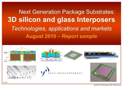
Next Generation Package Substrates:<br />
3D <strong>silicon</strong> <strong>and</strong> <strong>glass</strong> Interposers<br />
Technologies, applications <strong>and</strong> markets<br />
August 2010 – Report sample<br />
Courtesy of AAC<br />
© 2010<br />
Copyrights © Yole Développement SARL. All rights reserved.
Table of contents<br />
1. Scope of the report & definitions<br />
…………………………………….……………… 2<br />
2. Executive summary……………………..……21<br />
3. Applications <strong>and</strong> drivers…………………….40<br />
1. Interposers for MEMS & sensors………………………..45<br />
2. Logic <strong>interposers</strong>…………………………………………..52<br />
3. Logic + memory <strong>interposers</strong>……………………………..69<br />
4. Interposers for CMOS image sensors………………….80<br />
5. 3D <strong>silicon</strong> submounts for HB LEDs…………………….90<br />
6. 3D Power/RF/analogue integrated passives………….99<br />
7. Interposers fpr memory stacks………………………….108<br />
8. Misc. Glass/<strong>silicon</strong> package substrates………………114<br />
4. Technologies of 3D <strong>silicon</strong>/<strong>glass</strong><br />
<strong>interposers</strong>……………………………………130<br />
– Substrate materials, substrate thickness, routing metal,<br />
routing layers, dielectrics, patterning method, via drilling<br />
<strong>and</strong> filling, wafer <strong>and</strong> panel sizes………………………132<br />
– Technology preferences by application……………..166<br />
– Design rules………………………………………………..179<br />
5. Competing solutions <strong>and</strong> technologies by<br />
application segment…………………………..178<br />
6. Cost………………………………………………189<br />
– Cost structure of <strong>silicon</strong> <strong>interposers</strong> <strong>and</strong> influential<br />
parameters<br />
– Acceptable « prices », cost targets<br />
– Cost down roadmaps<br />
– Case examples<br />
7. Suppy chain analysis…………………………206<br />
– Critiacal review of the likely interposer manufacturers <strong>and</strong><br />
supply chain organization by application segment<br />
– Declared or visible players <strong>and</strong> their respective positions<br />
8. Market forecasts……………………………….220<br />
– 2009-2015 market forecasts In M$ by application, substrate<br />
material size <strong>and</strong> shape<br />
– 2009-2015 wafer forecasts in kWafers (wspy) by application,<br />
substrate material size <strong>and</strong> shape<br />
9. Roadmaps…………………………………….. 227<br />
10. Conclusions……………………………………234<br />
Component<br />
(optional)<br />
Substrate (wafer form, generally 6 inch or 8 inch,<br />
<strong>glass</strong> or Si or sapphire, …)<br />
TSV<br />
© 2010• 2<br />
Copyrights © Yole Développement SARL. All rights reserved.
This is the first ever report dedicated to 3D (si/<strong>glass</strong>) <strong>interposers</strong><br />
Why this report ? (1)<br />
• Semiconductor packaging has evolved considerably for the past 10 years, motivated by:<br />
– The continuous need for system miniaturization<br />
– The continuation of Moore’s law <strong>and</strong> the growing gap between <strong>silicon</strong> fine geometries <strong>and</strong> packaging substrates’<br />
relative coarse definitions<br />
– The continuously increasing gap between printed circuit boards <strong>and</strong> integrated circuits, both in terms of geometries<br />
<strong>and</strong> materials<br />
• As a consequence, System-in-Package (SiP), Package-on-package (PoP), flip-chip Ball grid Array (fc-BGA)<br />
or wafer-level packaging (WLP) techniques developped <strong>and</strong> considerably grew in the past years. WLP<br />
uses (usually partly amortized) <strong>silicon</strong> wafer fab equipments <strong>and</strong> techniques (photolithography) <strong>and</strong><br />
allows for<br />
– Chip-scale packaging <strong>and</strong> very high routing densities<br />
• More recently, the emergence of through <strong>silicon</strong> vias introduced the possibility to extend the capabilities<br />
of <strong>silicon</strong>/<strong>glass</strong> <strong>interposers</strong> to the 3rd dimension<br />
• As a consequence, the so-called mid-end infrastructure consisting in foundries for wafer-level packaging<br />
operations have developed at an unprecedented pace over the past 3 years to meet the growing dem<strong>and</strong><br />
for Wafer-Level Chip-Scale Packaging (or “fan-in WLCSP”) <strong>and</strong> flip-chip. These new facilities, half way<br />
between front-end foundries <strong>and</strong> regular assembly <strong>and</strong> packaging facilities, now support high volume<br />
manufacturing on large size wafers, thus permitting economies of scale.<br />
• 3D (<strong>silicon</strong> or <strong>glass</strong>) <strong>interposers</strong> combine wafer-level techniques <strong>and</strong> advantages with 3D routing<br />
capabilities. They now enter the competitive arena of package substrates <strong>and</strong> propose new growth<br />
opportunities for the now established mid-end infrastructure.<br />
© 2010• 3<br />
Copyrights © Yole Développement SARL. All rights reserved.
This is the first ever report dedicated to 3D (si/<strong>glass</strong>) <strong>interposers</strong><br />
Why this report ? (2)<br />
• However, it is not clear yet for the industry what the sweet spots for these 3D <strong>interposers</strong><br />
will be<br />
– for which applications?<br />
– Will the acceptable price exceed the manufacturing cost?<br />
– Will it be an intermediate step to 3D TSV’s in active IC’s, or is it a long term trend?<br />
– How will the supply chain evolve to serve this emerging market?<br />
– What will be the market size in the coming years?<br />
• Indeed, whereas this seems a very attractive market with looming ahead opportunities, <strong>and</strong> as we were compiling the data<br />
for this report, Sixis, a wholly-dedicated company to <strong>silicon</strong> <strong>interposers</strong>, was declared insolvent, shedding a different light<br />
on this emerging trend of the semiconductor packaging industry.<br />
• These are the questions we address in this first-ever dedicated report on 3D<br />
<strong>glass</strong>/<strong>interposers</strong>.<br />
• In the report, we list all the 3D interposer opportunities by application, <strong>and</strong> we analyze the<br />
drivers <strong>and</strong> expected benefits, as well as the alternative options. We make the case for some<br />
realistic interposer technology options by comparing their expected costs to acceptable<br />
market prices. We list some industry players involved in the 3D <strong>interposers</strong> field <strong>and</strong> we<br />
synthesize what we clearly see as the latest supply chain related moves. Finally, we propose<br />
a market roadmap <strong>and</strong> associated forecasts.<br />
© 2010• 4<br />
Copyrights © Yole Développement SARL. All rights reserved.
Definitions of « interposer »<br />
• 1994 National Technology Roadmap for<br />
Semiconductors :<br />
an electrical interconnection structure used between<br />
a <strong>silicon</strong> integrated circuit die <strong>and</strong> package, test jig,<br />
or other die that enables a reduced contact pad pitch<br />
on the die.<br />
• Wikipedia: An interposer is an electrical interface<br />
routing between one socket or connection to another.<br />
The purpose of an interposer is to spread a<br />
connection to a wider pitch or to reroute a<br />
connection to a different connection.<br />
Interposer comes from the Latin, interpōnere,<br />
meaning 'to put between.' [2]<br />
– A common example of an interposer is an integrated circuit die<br />
to BGA, such as in the Pentium II. This is done through<br />
various substrates, both rigid <strong>and</strong> flexible, most commonly<br />
FR4 for rigid, <strong>and</strong> polyimide for flexible. [1]<br />
© 2010• 5<br />
Copyrights © Yole Développement SARL. All rights reserved.
Our definition of 3D <strong>silicon</strong>/<strong>glass</strong><br />
<strong>interposers</strong><br />
• There is no normed definition as of today<br />
• Our definition<br />
– A 3D <strong>silicon</strong>/<strong>glass</strong> interposer is an interposer<br />
(see definitions on previous slide) which is<br />
• Made of <strong>silicon</strong> or <strong>glass</strong><br />
• Synonyms<br />
• Equipped with vertical through via electrical<br />
connections<br />
• Patterned by photolithography<br />
– Silicon/<strong>glass</strong> carriers, substrates<br />
• Different types of <strong>silicon</strong>/<strong>glass</strong> 3D <strong>interposers</strong><br />
Use of an organic multilayer interposer for<br />
BGA packaging use<br />
– 3D Silicon/<strong>glass</strong> <strong>interposers</strong> may embed various built-in components:<br />
• Passive components, zener diodes, some transistors (level shifting, buffering).<br />
– We will need in the future to set a scope definition boundary between 3D integrated<br />
circuits <strong>and</strong> 3D <strong>silicon</strong>/<strong>glass</strong> carriers. For the time being, this limit is still unclear.<br />
© 2010• 6<br />
Copyrights © Yole Développement SARL. All rights reserved.
Who should be interested in this report?<br />
Integrated semiconductor Device Manufacturers <strong>and</strong> fabless semiconductor<br />
companies<br />
– Visualize the drivers <strong>and</strong> expected benefits by application of 3D <strong>silicon</strong>/<strong>glass</strong> <strong>interposers</strong> as well as the alternative options<br />
– -enchmark the industrialization status of 3D <strong>glass</strong>/<strong>silicon</strong><br />
– Identify possible partnership /or second source packaging subcontractors for your forthcoming developments<br />
Assembly <strong>and</strong> Test Service companies<br />
– Get the list of the main companies involved in 3D <strong>silicon</strong>/<strong>glass</strong> <strong>interposers</strong> development <strong>and</strong> industrialization<br />
- creen possible new applications <strong>and</strong> technologies to support diversification strategy with 3D <strong>silicon</strong>/<strong>glass</strong> <strong>interposers</strong><br />
Silicon Wafer foundries<br />
– creen possible new applications <strong>and</strong> technologies to support diversification strategy with 3D <strong>silicon</strong>/<strong>glass</strong> <strong>interposers</strong>,<br />
especially by loading aging facilities<br />
Equipment <strong>and</strong> Material suppliers<br />
– -Underst<strong>and</strong> the differentiated value of your products <strong>and</strong> technologies in this emerging but fast growing market<br />
– Identify new business opportunities <strong>and</strong> prospects<br />
Electronic module makers <strong>and</strong> Original Equipment Makers<br />
– Evaluate the availability <strong>and</strong> benefits of using 3D <strong>silicon</strong>/<strong>glass</strong> <strong>interposers</strong> in your end system<br />
– Monitor different 3D <strong>silicon</strong>/<strong>glass</strong> <strong>interposers</strong> suppliers to adjust your sourcing strategy<br />
PCB <strong>and</strong> IC substrate manufacturers<br />
– Monitor the evolution of IC packaging, assembly <strong>and</strong> test, especially linked to the emerging 3D <strong>silicon</strong>/<strong>glass</strong> <strong>interposers</strong><br />
– Measure the threat of 3D <strong>silicon</strong>/<strong>glass</strong> <strong>interposers</strong> to the established PCB interposer <strong>and</strong> substrate businesses<br />
– Screen possible new applications <strong>and</strong> technologies to support diversification strategy with 3D <strong>silicon</strong>/<strong>glass</strong> <strong>interposers</strong><br />
© 2010• 7<br />
Copyrights © Yole Développement SARL. All rights reserved.
Companies cited throughout the report<br />
AAC Microtec, Allvia, AMD, Altera, Amkor Technology, apm, ASE, ASET,<br />
Avago Technologies, Bridgelux, CEA-LETI, ChipMOS, Cree, Corning, Dai<br />
Nippon Printing, Dalsa, Discera, Elpida, Epcos, Epistar, EPWorks,<br />
Fraunhofer IZM, Georgia Tech, Hitachi , Hymite, Hynix, Ibiden, IBM, IME,<br />
IMT, Infineon Technologies, Intel, Ipdia, Liquid Design Solutions, LG<br />
Innotek, Lumileds, Maxim, Micron, Nanium, National semiconductor, NEC<br />
/ Schott, Nepes, Nichia, Nippon Electric Glass, Nokia, NXP<br />
Semiconductors, On Semiconductors, Panasonic, Qualcomm, Renesas,<br />
Replisaurus Technologies, Samsung, Schott, Sensonor, Shinko Electric,<br />
Silex Microsystems, SMIC, Soitec, Sony, StatsChipPac, STEricsson,<br />
STMicroelectronics, Süss Microtec, Tecnisco, Texas Instruments, TMT,<br />
Toshiba, TSMC, UltraTech, UMC, UTAC, VTI Technologies, WLCSP,<br />
Xilinx, Xintec<br />
© 2010• 8<br />
Copyrights © Yole Développement SARL. All rights reserved.
Historical account<br />
From 2D to 3D <strong>silicon</strong>/<strong>glass</strong> <strong>interposers</strong><br />
• Some companies promote<br />
2.5D <strong>interposers</strong> so as to optimize the<br />
use of the various technology nodes<br />
at their maximum integration potentials<br />
according to the functions to be<br />
designed, for example:<br />
– Digital on CMOS 28nm<br />
– RF on CMOS 90nm<br />
– PMU on CMOS 130nm<br />
• However, since many SoC’s are already<br />
packaged by flip-chip, the opportunity to<br />
turn back to wire bonds is questionable,<br />
<strong>and</strong> true 3D <strong>silicon</strong>/<strong>glass</strong> <strong>interposers</strong> may well be needed<br />
in the near future for high IO count / high IO<br />
toggling frequency devices.<br />
Courtesy of ASE<br />
Courtesy of STMicroelectronics<br />
© 2010• 9<br />
Copyrights © Yole Développement SARL. All rights reserved.
The evolution of semiconductor packaging: a bridging<br />
technology between ICs <strong>and</strong> PCBs<br />
Feature sizes of PCBs<br />
Feature sizes of CMOS transistors<br />
100µm<br />
Organic <strong>interposers</strong><br />
3D integration<br />
Bumping<br />
28nm<br />
© 2010• 10<br />
1970<br />
through<br />
hole<br />
technology<br />
1980<br />
Surface mount<br />
devices<br />
Copyrights © Yole Développement SARL. All rights reserved.<br />
1990<br />
CSPs/BGAs<br />
SiPs<br />
2000<br />
2010<br />
WLCSP<br />
3DIC<br />
more SiPs<br />
TSV<br />
Flip-chip BGA<br />
Fan-out WLCSP<br />
PoP,<br />
Integrated Passive Devices<br />
Silicon <strong>interposers</strong>
The evolution of substrate technologies<br />
• In the next 5 years, packaging substrates are expected to integrate significantly higher pin counts<br />
<strong>and</strong> embedded active <strong>and</strong> passive devices within System in Package (SiP) configurations.<br />
• Minimum line width will shrink to 5 microns with less than 30 microns to 5 microns via diameters:<br />
– To fabricate such ultra higher density packaging substrate, current PWB process technology will face to technology<br />
limitation Possibility to introduce <strong>silicon</strong> interposer <strong>and</strong>/or <strong>glass</strong> interposer like LCD panel to fabricate less than 5<br />
microns wiring with much smaller via diameters.<br />
2000 – 2005 2006 – 2010<br />
Technology Driver<br />
(Min. Line Width)<br />
30µm – 15µm<br />
Flip Chip<br />
15µm - 5µm - 3µm<br />
Flip Chip, EAD/EPD for SiP<br />
Via Diameter 75µm – 50µm 30µm – 5µm<br />
Capital Investment $0.15 – $0.20 Billion US$ 0.20 – 0.50 Billion<br />
Major Process<br />
Semi Additive<br />
Semi Additive. Silicon Technology & LCD<br />
Technology (Glass Substrates)<br />
Bus Frequency 8000 MHz – 1.2 GHz > 10 GHz<br />
Package Type<br />
CSP, WL-CSP<br />
PoP, CSP, BGA/CSP with Embedded Active &<br />
Passive Devices<br />
PWB Type Builup PWB, FPC, FRPC Silicon &/or Glass Interposer, Buid-up PWB<br />
Application driver<br />
Cellular phone, Digital Home Appliances,<br />
Broad-b<strong>and</strong> Internet<br />
Digital TV, Smart Phones, Digital Home<br />
Appliance<br />
Profit Structure High Added Value & Differentiate High Added Value & Differentiate<br />
Business Model<br />
Core Competence + Horizontal Division of<br />
Labor<br />
Core Competencies + Strategic Alliance + New<br />
Concept<br />
© 2010• 11<br />
Copyrights © Yole Développement SARL. All rights reserved.
More Silicon Value is Moving to the Package!<br />
• A recent trend increasing these days are 3D <strong>interposers</strong>:<br />
– Based on <strong>silicon</strong> or <strong>glass</strong>, 3D <strong>interposers</strong> are a next generation substrate technology which aims at<br />
replacing traditional PCB laminate or ceramic technologies for the sake of extreme miniaturization<br />
<strong>and</strong> performance. This type of “intermediate 3D” is perceived as a “bridge” platform between today’s<br />
2D <strong>and</strong> future genuine 3D that will start beyond 2012-2013. Specific features like the integration of<br />
mature logic <strong>and</strong> analog functions such as IPD (integrated passive devices) will be key components<br />
in the effective commercialization of 3D <strong>interposers</strong> in the short term.<br />
• 3D integration opens up a possible supply chain value change to all players:<br />
– As more <strong>and</strong> more value is now moving to the package in general. IDMs, Fab-less players, wafer<br />
Foundries, packaging houses, MEMS players, substrate <strong>and</strong> PCB suppliers are all poised to take on<br />
more value in this new era if they all prepare for the investments it requires!<br />
3D Silicon interposer<br />
Logic IC<br />
28-32nm<br />
Low-k<br />
100µm pitch<br />
200µm pitch<br />
BGA<br />
laminate<br />
PMU<br />
PCB<br />
0.4mm pitch<br />
© 2010• 12<br />
Copyrights © Yole Développement SARL. All rights reserved.
Silicon/<strong>glass</strong> 3D <strong>interposers</strong> technology segments<br />
• By studying exhaustively solutions<br />
currently in production as well as under<br />
development, we identified the following<br />
technology segments for 3D <strong>interposers</strong>:<br />
3D MEMS<br />
capping<br />
interposer<br />
PCB<br />
MEMS device<br />
1. MEMS <strong>and</strong> sensors capping <strong>interposers</strong><br />
2. Logic only <strong>interposers</strong><br />
3. Logic + memory <strong>interposers</strong><br />
4. CMOS image sensors <strong>interposers</strong><br />
5. HB-LED <strong>silicon</strong> submounts<br />
6. 3D Power/RF/analogue integrated<br />
passive <strong>interposers</strong><br />
7. Memory stack <strong>interposers</strong><br />
8. Miscellaneous <strong>silicon</strong>/<strong>glass</strong><br />
substrates/packages<br />
BGA<br />
laminate<br />
3D Silicon<br />
interposer<br />
PCB<br />
3D<br />
interposer 2<br />
3D<br />
Power/RF/analogue<br />
IPD<br />
PCB<br />
PMU<br />
Logic IC<br />
28-32nm<br />
IC2<br />
IC1<br />
Low-k<br />
100µm pitch<br />
200µm pitch<br />
0.4mm pitch<br />
IC1<br />
IC2<br />
3D Silicon<br />
submount<br />
with ESD<br />
protection<br />
PCB<br />
DRAM<br />
Interposer<br />
Logic<br />
LED<br />
3D<br />
interposer 1<br />
PCB or BGA laminate<br />
© 2010• 13<br />
Copyrights © Yole Développement SARL. All rights reserved.
PMU<br />
Summary table - 2010 Status of 3D <strong>silicon</strong>/<strong>glass</strong> <strong>interposers</strong><br />
an emerging market<br />
3D MEMS<br />
capping<br />
interposer<br />
PCB<br />
MEMS device<br />
3D Silicon<br />
submount<br />
with ESD<br />
protection<br />
PCB<br />
LED<br />
3D Silicon<br />
interposer<br />
/IPD<br />
PCB<br />
RF or analog or<br />
logic IC<br />
3D Silicon<br />
interposer<br />
BGA<br />
laminate<br />
PCB<br />
Logic IC<br />
28-32nm<br />
Low-k<br />
100µm pitch<br />
200µm pitch<br />
0.4mm pitch<br />
Logic<br />
Interposer<br />
interposer<br />
DRAM<br />
Interposer<br />
type<br />
(technology<br />
segments)<br />
MEMS <strong>and</strong><br />
sensors<br />
capping<br />
<strong>interposers</strong><br />
CMOS<br />
image<br />
sensors<br />
<strong>interposers</strong><br />
HB-LED<br />
<strong>silicon</strong><br />
submounts<br />
3D<br />
Power/RF/<br />
analogue<br />
integrated<br />
passive<br />
<strong>interposers</strong><br />
Logic only<br />
<strong>interposers</strong><br />
Logic +<br />
memory<br />
<strong>interposers</strong><br />
Memory<br />
stack<br />
<strong>interposers</strong><br />
Misc.<br />
Silicon/<strong>glass</strong><br />
substrates/<br />
packages<br />
Applications<br />
gyroscopes,<br />
accelerometers,<br />
microphones,<br />
pressure sensors,<br />
RF-MEMS ,<br />
microfluidic, microprobes,<br />
optical<br />
CIS (in mobile<br />
phones, cameras,<br />
automotive)<br />
HB-LED/ UHB-LED<br />
(mobile, automotive,<br />
general lighting)<br />
RF transceivers <strong>and</strong><br />
power amplifiers<br />
(mobile phones,<br />
medical & industrial)<br />
High IO count logic<br />
IC’s: CPU’s, GPU’s,<br />
FPGA’s, application<br />
processors<br />
Application<br />
processors for mobile<br />
phones, CPU’s,<br />
GPU’s<br />
Server farms,<br />
computers, both<br />
DRAM’s <strong>and</strong> flash<br />
memories<br />
Medical, industrial, oil<br />
search, aerospace,<br />
defence<br />
2010 status In Production Sampling. Will<br />
appear with<br />
BSI. Sony<br />
already in BSI,<br />
w/o <strong>interposers</strong><br />
Some early<br />
production<br />
Sampling<br />
(similar<br />
<strong>interposers</strong>, but<br />
w/o TSVs are in<br />
production)<br />
Proofs of<br />
concepts<br />
In-development,<br />
proofs of<br />
concept<br />
In-development,<br />
start of prod by<br />
year end<br />
Development of<br />
demonstrators<br />
Wafer size 150-200mm 300mm 150-200mm 150-200mm 300mm 300mm 200mm 150-200mm<br />
2010 Wafers 183k (86-inch)<br />
44k (8-inch)<br />
0 50k (6-inch eq.) A few hundreds 0 0 A few k’s A few hundreds<br />
Players (nonexhaustive)<br />
© 2010• 14<br />
Copyrights © Yole Développement SARL. All rights reserved.
3D <strong>silicon</strong>/<strong>glass</strong> typical interposer structure<br />
& definitions<br />
Generic Cross-section drawing<br />
UBM (under Bump Metallurgy)<br />
Metal (Al or AlSiCu or Cu or W)<br />
ILD (Inter Layer Dielectric, SiO2 or Si3N4 or polymer…)<br />
Dielectric passivation (Polyimide, BCB, epoxy, AL-X)<br />
Front-side back-end of line<br />
Fine-pitch (50µm) bumps<br />
Component<br />
(optional)<br />
Back-side back-end of line<br />
Substrate (<strong>glass</strong> or Si)<br />
Fine-pitch (50µm) bumps<br />
TSV<br />
© 2010• 15<br />
Copyrights © Yole Développement SARL. All rights reserved.
3D <strong>silicon</strong>/<strong>glass</strong> interposer technology options<br />
The average interposer is rather …<br />
Substrate material<br />
<strong>silicon</strong><br />
<strong>glass</strong><br />
Substrate thickness<br />
Processing base<br />
thin<br />
thick<br />
20µm 50µm 100µm 200µm<br />
Wafers<br />
Others (panels, …)<br />
Substrate<br />
wafer size, if wafers<br />
Amount of front side<br />
routing metal layers<br />
Amount of back side<br />
routing metal layers<br />
6 inch 8 inch<br />
1ML<br />
0ML<br />
2ML<br />
1ML<br />
3ML<br />
2ML<br />
12 inch<br />
4+ML<br />
3+ML<br />
Patterning method photolithography other<br />
Photolithography<br />
equipment<br />
Planarization of<br />
metal layers<br />
Via etching/drilling<br />
stepper<br />
CMP (copper<br />
damascene)<br />
Dry etching (DRIE)<br />
Mask aligner<br />
No planarization<br />
Laser drilling, other<br />
Back-end<br />
of line<br />
Via filling material<br />
Embedded<br />
components<br />
© 2010• 16<br />
Copper<br />
Embedded components<br />
(capacitors, inductors, diodes,…)<br />
Copyrights © Yole Développement SARL. All rights reserved.<br />
Tungsten, gold, other<br />
No embedded<br />
components<br />
Vias
3D Silicon interposer Case example #1:<br />
220µm pitch Flip-chip down to 1.0mm PCB (3/4)<br />
FC-BGA solution (1+2+1)<br />
for 220µm pitch Flip-chip to 1.0mm PCB<br />
3D interposer solution<br />
Interposer (Glass or Silicon)<br />
+ cheap BGA (2 layers) solution<br />
Logic SOC<br />
Logic SOC<br />
PMU<br />
PCB<br />
1.0mm pitch<br />
PCB<br />
1.0mm pitch<br />
TOT Packaging COST = $2.40<br />
TOT Packaging COST = $1.9 - $2.1 !<br />
© 2010• 17<br />
Copyrights © Yole Développement SARL. All rights reserved.
3D interposer COST<br />
3D Silicon interposer * Case example #1:<br />
220µm pitch Flip-chip down to 1.0mm PCB<br />
$1 600<br />
$1 400<br />
$1 200<br />
$1 000<br />
$800<br />
$600<br />
3D interposer COST target to reach parity with<br />
FC-BGA equivalent solution (for Application #1)<br />
Yole Developpement © April 2010<br />
P<br />
C<br />
B<br />
Logic<br />
SOC<br />
1.0mm<br />
pitch<br />
$1 500<br />
* 3D Interposer<br />
cost include metal<br />
vias + RDL<br />
$400<br />
$200<br />
$0<br />
$265<br />
200mm interposer<br />
Cost Target<br />
X<br />
Cost target<br />
difficult to reach<br />
$570<br />
300mm interposer<br />
Cost Target<br />
?<br />
Could be possible on<br />
optimized infrastructure<br />
'Panel' interposer<br />
Cost Target<br />
Technology of choice<br />
but immature infrastructure!<br />
© 2010• 18<br />
Copyrights © Yole Développement SARL. All rights reserved.
wafers (x1000)<br />
4500<br />
3D <strong>silicon</strong>/<strong>glass</strong> <strong>interposers</strong> wafer forecasts<br />
Silicon Interposers market<br />
forecasts<br />
4000<br />
3500<br />
3000<br />
2500<br />
2000<br />
1500<br />
1000<br />
500<br />
0<br />
2009 2010 2011 2012 2013 2014 2015<br />
300mm interposer wafers for CMOS Image Sensors (x1000)<br />
150mm 3D <strong>glass</strong>/<strong>silicon</strong> interposer wafers for MEMS & sensors (x1000)<br />
200mm 3D <strong>glass</strong>/<strong>silicon</strong> interposer wafers for MEMS & sensors (x1000) 300mm 3D <strong>glass</strong>/<strong>silicon</strong> interposer wafers for MEMS & sensors (x1000)<br />
150mm 3D LED <strong>silicon</strong> submounts (x1000)<br />
200mm 3D LED <strong>silicon</strong> submounts (x1000)<br />
300mm 3D LED <strong>silicon</strong> submounts (x1000)<br />
150mm 3D Integrated Passive Devices for RF/Power/analogue (x1000)<br />
200mm 3D Integrated Passive Devices for RF/Power/analogue (x1000) Total 3D 300mm 3D interposer wafers for CPUs (x1000)<br />
Total 3D 300mm 3D interposer wafers for GPUs (x1000)<br />
3D <strong>silicon</strong>/<strong>glass</strong> 300mm interposer wafers for phone processors (x1000)<br />
300mm 3D interposer wafers for logic+memory (x1000)<br />
300mm 3D <strong>glass</strong>/<strong>silicon</strong> interposer wafers for DRAM stacks (x1000)<br />
300mm 3D <strong>glass</strong>/<strong>silicon</strong> interposer wafers for FLASH stacks (x1000) Misc. Silicon/<strong>glass</strong> 3D substrates/packages (300mm eq. x1000 wafers)<br />
© 2010• 19<br />
Copyrights © Yole Développement SARL. All rights reserved.
About the Authors of this Report<br />
• Jean-Marc Yannou:<br />
– Jean-Marc is in charge of advanced packaging analyses at<br />
Yole Développement, including Wafer Level Packaging <strong>and</strong> 3D<br />
System Integration. He has 15-years of experience in the<br />
semiconductor industry. He worked for Texas Instruments <strong>and</strong><br />
Philips (then NXP semiconductors) where he served as<br />
“Innovation Manager” for System-in-Package technologies<br />
• Jerome Baron:<br />
– Jerome is leading the MEMS <strong>and</strong> Advanced Packaging market<br />
research at Yole. He has been involved in the technology<br />
analysis of the 3D packaging market evolution at device,<br />
equipment <strong>and</strong> material supplier levels. He was granted a<br />
Master of Science degree in Nanotechnologies from the<br />
National Institute of Applied Sciences in Lyon, France<br />
© 2010• 20<br />
Copyrights © Yole Développement SARL. All rights reserved.


